Note: Descriptions are shown in the official language in which they were submitted.
2159762
FIELD OF THE INVENTION
This invention relates to clock generation
circuitry and in particular to a frequency synthesizer
the duty cycle of which can be controlled for more than
one frequency.
BACKGROUND TO THE INVENTION
Modern high speed video graphics display
circuitry utilize pipelining technology which use both
the rising and falling edges of an input clock signal in
order to achieve short pipeline delay, high operating
frequency and low power dissipation within a given
semiconductor fabricating process. Digital logic
circuits along the pipeline make use of time elapsed
between the rising and falling edges to manipulate data.
For two digital logic circuits with propagation
delays tdl and td2 to operate properly within high and
low logic level pulse intervals respectively, the duty
cycle of the clock must be exactly (tdl(tdl+td2)), or
else the clock signal has to run at a lower frequency
since any other value of duty cycle requires either a
longer high pulse width or longer low pulse width, and
in turn, a longer cycling period, to maintain proper
functionality within the two particular logic circuits.
Further, to perform a maximum number of logic
operations within a certain period of time, a high
performance video graphics display system requires more
than one synthesized clock to run at different clocking
frequencies with different duty cycles at which all the
digital logic circuits are operating properly, and so
that no part of any clock cycle is wasted.
The duty cycle of the clock signal of a
frequency doubler has been successfully controlled, but
a frequency doubler is incapable of synthesizing more
than one frequency from a given reference frequency.
'~ ~ 21597fi2
The frequency doubler also must operate at a relatively
low frequency.
Digital circuits have also been employed to
achieve duty cycle control at the output of a frequency
synthesizer, but programming range has been inadequate
because of the relatively higher slew rate at digital
logic circuit outputs.
BACKGROUND TO THE INVENTION
The present invention is a frequency
l0 synthesizer which generates different output frequencies
from a single source of reference frequency, wherein the
output duty cycles are programmable. The invention has
provided programmable duty cycle clock signals at a very
high frequency of 200 MHz. The invention is thus suited
for use in the aforenoted video graphic display
circuitry.
In accordance with an embodiment of the
invention, a programmable frequency synthesizer is
comprised of a phase locked loop (PLL) including a
current control oscillator (ICO) which generates a
digital clock signal, the frequency of which is
controlled by input current to the ICO, a level
translator which has a finite output slew rate for
translating reduced swing output signals from the ICO
into fully digital signals, an output buffer for
buffering the output of the level translator, a
reference source of clock signals, a phase-frequency
detector (PFD) for receiving output signals from the
reference source and the output from the output buffer
and for generating voltage pulse signals having pulse
widths which are directly proportional to phase
difference between the signals from the reference source
and the output signals from the output of the output
buffer, a charge pump for converting output voltage
pulses from the PFD into output current pulses, a loop
2
2159762
filter for converting output current pulses from the
charge pump into a bias voltage and for providing the
PLL with high order damping, a voltage to current
converter for mapping the output bias voltage from the
loop filter into bias current applied to the ICO for
control thereof, and apparatus for varying the slew rate
of the output signals from the level translator wherein
the duty cycle of the output signals may be varied. The
output buffer may be included as part of the level
translator which may be, in turn, included as part of
the ICO.
In accordance with another embodiment of the
invention, a programmable frequency synthesizer is
comprised of a phase locked loop (PLL) including a
current controlled oscillator (ICO) which has an
internal signal with a finite slew rate, a reference
source of clock signals, a phase-frequency detector
(PFD) for receiving output signals from the reference
source and the output from the ICO and for generating
voltage pulse signals having pulse widths which are
directly proportional to phase difference between the
signals form the reference source and the output signals
from the output from the ICO, a charge pump, for
converting output voltage pulses from the PFD into
output current pulses, a loop filter for converting
output current pulses from the charge pump into a bias
voltage and for providing the PLL with high order
damping, a voltage to current converter for mapping the
output bias voltage from the loop filter into bias
current that controls the ICO, and apparatus for varying
the slew rate of a signal within the ICO wherein the
duty-cycle of the output signals may be varied. The
voltage to current converter may combine with the ICO
and become a voltage controlled oscillator (VCO).
3
2I~9~62
In accordance with another embodiment of the
invention, a programmable frequency synthesizer is
comprised of a phase locked loop (PLL) including a
voltage controlled oscillator (VCO) which has an
internal signal with a finite output slew rate, a
reference source of clock signals, a phase-frequency
detector (PFD) for receiving output signals from the
reference source and the output from the VCO and for
generating voltage pulse signals having pulse widths
which are directly proportional to phase difference
between the signals from the reference source and the
output signals from the output from the VCO, a charge
pump for converting output voltage pulses from the PFD
into output current pulses, a loop filter for converting
output current pulses from the charge pump into a bias
voltage and for providing the PLL with high order
damping, a voltage to current converter for mapping the
output bias voltage from the loop filter into bias
current that controls the ICO, and apparatus for varying
the slew rate of a signal within the VCO wherein the
duty-cycle of the output signals may be varied.
In accordance with an embodiment of the
invention, a programmable frequency synthesizer is
comprised of a phase locked loop (PLL) including a
current controlled oscillator (ICO), a level translator
for receiving output signals from the ICO wherein the
output signals have a finite slew rate, a reference
source of signals, a phase-frequency detector for
receiving signals from the reference source and output
signals generated by the level translator and for
providing pulse signals to the ICO having pulse widths
which are directly proportional to phase difference
between the signals from the reference source and the
output signals from the level translator, and apparatus
for varying the slew rate of the output signals from the
4
CA 02159762 1999-11-10
phase-frequency detector wherein the duty cycle of the
output signals may be varied.
In accordance with another embodiment, a
programmable frequency synthesizer is comprised of a
phase locked loop (PLL) including a current controlled
oscillator (ICO), a reference source of signals, a
phase-frequency detector for receiving signals from the
reference source and feedback signals from an output of
the phase locked loop derived from the output of the ICO
and for providing signals to the ICO having pulse widths
which are directly proportional to phase difference
between the signals from the reference source and the
feedback signals, and apparatus for varying the slew
rate of output signals from the ICO wherein the duty
cycle of the output signals may be varied.
In accordance with another embodiment, a method
of synthesizing a signal is comprised of providing a
phase locked loop having a controlled oscillator (CO),
and selectively varying the slew rate of an output
signal derived from CO within the loop or within the CO
to thereby vary the duty cycle thereof.
In accordance with another embodiment, a method
of synthesizing a signal is comprised of synthesizing a
pulse signal within a phase locked loop and selectively
varying the slew rate of the signal within the phase
locked loop to vary the duty cycle of the signal.
5
CA 02159762 1999-11-10
In accordance with another embodiment, a
programmable frequency synthesizer comprising a phase
locked loop (PLL) including a current control oscillator
(ICO) which generates a digital clock signal, the
frequency of which is controlled by input current to the
ICO, a level translator which has a finite output slew
rate for translating reduced swing output signals from
the ICO into fully digital signals, an output buffer
having an output for buffering the output of the level
translator, a reference source of clock signals, a
phase-frequency detector (PFD) for receiving output
signals from said reference source and the output from
the output buffer and for generating voltage pulse
signals having pulse widths which are directly
proportional to phase difference between the signals
from the reference source and the output signals from
the output of the output buffer, a charge pump for
converting output voltage pulses from the PFD into
output current pulses, a loop filter for converting
output current pulses from the charge pump into a bias
voltage and for providing the PLL with high order
damping, a voltage to current converter for mapping the
output bias voltage from the loop filter into bias
current applied to the ICO for control thereof, and
apparatus for varying the slew rate of the output
signals from the level translator wherein the duty cycle
of the output signals of said synthesizer may be varied.
In accordance with another embodiment, a
programmable frequency synthesizer comprising a phase
locked loop (PLL) including a current controlled
oscillator (ICO) which has an internal signal with a
finite slew rate, a reference source of clock signals, a
phase-frequency detector (PFD) for receiving output
signals from said reference source and the output from
5a
~
CA 02159762 1999-11-10
the ICO and for generating voltage pulse signals having
pulse widths which are directly proportional to phase
difference between the signals from the reference source
and the output signals from the ICO, a charge pump for
converting output voltage pulses from the PFD into
output current pulses, a loop filter for converting
output current pulses from the charge pump into a bias
voltage and for providing the PLL with high order
damping, a voltage to current converter for mapping the
output bias voltage from the loop filter into bias
current that controls the ICO, and apparatus for varying
the slew rate of a signal within the ICO wherein the
duty-cycle of the output signals may be varied.
In accordance with another embodiment, a
programmable frequency synthesizer comprising a phase
locked loop (PLL) including a voltage controlled
oscillator (VCO) which has an internal signal with a
finite output slew rate, a reference source of clock
signals, a phase-frequency detector (PFD) for receiving
output signals from said reference source and the output
from the VCO and for generating voltage pulse signals
having pulse widths which are directly proportional to
phase difference between the signals from the reference
source and the output signals from the VCO, a charge
pump for converting output voltage pulses from the PFD
into output current pulses, a loop filter for converting
output current pulses from the charge pump into a bias
voltage and for providing the PLL with high order
damping, a voltage to current converter for mapping the
output bias voltage from the loop filter into bias
current that controls the VCO, and apparatus for varying
the slew rate of a signal within the VCO wherein the
duty-cycle of the output signals of said synthesizer may
be varied.
5b
CA 02159762 1999-11-10
In accordance with another embodiment, a
method of synthesizing a signal comprising providing a
phase locked loop having a current controlled oscillator
(ICO), selectively varying the slew rate of an output
signal of the ICO to thereby vary the duty cycle
thereof, the selectively varying step including
selecting an amount of current derived from the output
signal of the ICO and providing the selected amount of
current to a feedback loop of the phase locked loop, the
selectively varying step is comprised of switching FETs
in parallel to carry said current derived from the
output signal, thereby sourcing increased current to the
feedback loop when an output voltage of the ICO is
rising, or draining increased current from the feedback
loop when the output voltage of the ICO is falling.
In accordance with another embodiment, a
method of synthesizing a signal comprising synthesizing
a pulse signal within a phase locked loop and
selectively varying the slew rate of said signal within
the phase locked loop to vary the duty cycle of said
signal, the phase locked loop including a voltage
controlled oscillator (VCO) and means for varying the
slew rate of a signal within the VCO.
BRIEF INTRC~T~T1CTT(~N TO THE DR.AWIT1~GS
A better understanding of the invention will
be obtained by readng the description of the invention
below, with reference to the following drawings, in
which:
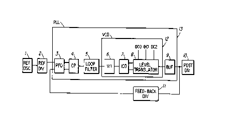
Figure 1 is a block diagram of a frequency
synthesizer system in accordance with the present
invention,
Sc
2159762
Figure 2 is a schematic diagram of a current
controlled oscillator which can be used in the present
invention,
Figure 3 is a block diagram of a level
translator which does not provide duty cycle control,
Figure 4 is a signal timing chart used to
illustrate operation of the present invention, and
Figure 5 is a block diagram of an improved
level translator that can be programmed and used in the
l0 present invention.
DETAILED DESCRIPTION OF THE INVENTION
In accordance with an embodiment of the
invention, Figure 1 illustrates a frequency synthesizer,
which includes a phase-locked loop (PLL) 13. A
reference oscillator 1 has its output signal divided
down by reference divider 2, the output signal of which
is applied to one of the pairs of inputs of a phase-
frequency detector 3 of a phase-locked loop. The output
of the detector 3 is applied to a charge pump 4. The
output signal of the charge pump 4 is applied through a
loop filter to a voltage to current converter 6 of a
voltage controlled oscillator (VCO) 12. In a successful
laboratory prototype, the loop filter was a second order
RC filter accompanied by a third order capacitor. The
loop filter converts the input current pulses into an
output bias voltage with high order damping. However
other filters could be used.
The output clock signals of the VCO is applied
to an output buffer 9. A feedback frequency divider 11
divides the output signal from the PLL and applies it to
another one of the inputs of a frequency-phase detector
3. The output of the buffer 9 also provides the output
signal of the PLL, and is typically applied to the input
of a post frequency divider 10. However other forms of
PLL and VCO could be used.
6
2~ 59 762
In accordance with an embodiment of the present
invention, a level translator which is programmable by
receiving program bits at inputs DCO, DC1 and DC2, for
example, selectively controls the slew rate of its
output, and thus the duty cycle of the signal
synthesized by the PLL, in a manner as will be described
below.
The output pulses of the phase-frequency
detector 3 have widths directly proportional to the
phase difference between the reference clock signal and
the fed-back signal from the output of the PLL 13. The
charge pump 4 sources or drains electronic charge to or
from its output in an amount which is determined by the
width of the input pulses from the phase-frequency
detector 3. The loop filter 5 converts electronic
charge from the charge pump into voltage level with high
order damping. The voltage controlled oscillator (VCO)
12 outputs a digital clock signal of which the frequency
is determined by the input voltage level to it. Buffer
9 is a high speed digital clock buffer which buffers the
output signal of the VCO.
The VCO includes a voltage to current converter
6 which sources a constant current into its output in
accordance with the input voltage level. Current
controlled oscillator 7 receives the output signal of
converter 6 and outputs a pair of reduced amplitude
swing differential clock signals of which the
frequencies are determined by the input current
magnitude. Level translator 8 receives the output
signal of the current controlled oscillator and converts
the reduced swing differential output signals and
converts them to a fully digital output clock signal
with the same frequency.
During frequency synthesizing, the clock
frequency at the output of the frequency synthesizer is
7
2~5976~
determined by the reference frequency oscillator and the
dividing ratios of the reference frequency divider 2,
the feedback divider 11, and the post divider 10. For
any fixed combination of the dividing ratios of these
dividers, and a fixed reference frequencies, the PLL in
accordance with the prior art will output a clock signal
of which the frequency is invariant in the time domain.
In that case, the VCO 12 takes a constant input voltage
level and generates a clock of which the frequency is
invariant in the time domain.
In the design described above, with a reference
oscillator 1 with frequency fi, a reference divider 2 of
frequency dividing ratio of M, a feed-back divider 11 of
frequency dividing ratio of N, and a post divider 10 of
frequency dividing ratio of P, a synthesized clock
signal of frequency given by fo=(fixN) / (MxP) will
present at the output of the post divider 10.
Other forms of frequency synthesizer may
alternatively be used.
It will be noted that the phase-frequency
detector has two inputs, a reference input and a feed-
back input, and two outputs, up and down. When clock
signals at the reference input lead the clock signals at
the feed-back input in phase, the output up will output
a voltage pulse the pulse width of which is directly
proportional to the phase lead. When clock signals at
the reference input lags the clock signals at the feed-
back input in phase, the down output will output a
voltage pulse the pulse width of which is directly
proportional to the phase lag.
Figure 2 illustrates a design of a current
controlled oscillator which can be used as element 7. A
controllable input current source 15 from (voltage to
current converter 6) supplies operating current to a
ring oscillator, the ring oscillator being comprised of
8
2~ 58762
a series of inverters I1 - I5 in this example. This
circuit generates a reduced swing clock signal in the
output nodes N1 - N5 of each of the five oscillating
elements. the frequency of each clock signal is
identical in symmetry, and is given, for example, by the
reciprocal of ten times the oscillating element
propagation delays which is a function of the current
supplied from the current source 15.
In a laboratory prototype, because there were
five identical inverters in the ring, each inverter
output a reduced swing clock signal the phase of which
led the output of the following inverter by 216 degrees.
The magnitude of the reduced-swing clock signal
at the output nodes of each inverter is determined by
the input current in such a relation that the higher the
input current into the ICO, the larger is the oscillator
frequency. A logic 0 level of the swing is the system
ground value VSS, while the logic 1 level of the swing
is limited by the operation of the ICO to a voltage
which ranges from the minimum supply voltage for
oscillation that can possibly occur among the five
inverters or the maximum voltage for the previous
voltage to current converter 6 to maintain a constant
current into the ICO. Differential outputs are taken
from the ICO at nodes N3 and N4, or at the output nodes
of any other two consecutive oscillating elements. It
may be seen that a differential output signal can be
obtained from the output nodes of any serial connected
odd number of inverters, for a particular design which
requires the delay between the differential output
signal components. However, for the present embodiment,
the odd number of inverters is 5.
In the present specification, the differential
output signals and the nodes at which they appear are
A
~~5976~
labeled S+ and S- respectively. These signals are
reduced swing clock signals of which the frequency is
determined by the input current level of the ICO 7. In
a laboratory prototype, S+ led S- by a phase of 216
degrees.
Figure 3 illustrates a basic level translator
which does not have the ability to provide output slew
rate control, and thus duty cycle control. A
description thereof will be given as background in order
to better understand the present invention. The
translator (and the improved translator used in the
present invention) is preferably fabricated using metal
oxide silicon field effect transistors (MOSFETs).
A differential input stage of the level
translator is formed of two n-channel MOSFETs, Ml and
M2, the gates of which are connected to receive the S+
and S- signals respectively of the current controlled
oscillator. The bulks (substrates) and sources of the
MOSFETs are connected together and to the system ground
VSS. The drain node of MOSFET M1, denoted as N0, is
connected to the drain node of MOSFET M3, and is
connected to the gates of MOSFETs M3 and M4. MOSFETs M3
and M4 are two p-channel MOSFETs configured as a current
mirror, with their substrates and sources connected
together and to the power supply VDD. The output signal
of the level translator appears at node OUT, which is
formed by connecting the drain nodes of MOSFETs M2 and
M4.
Operation of the level translator will be
understood by a consideration of Figure 4. The
operation of the level translator is periodic, since the
input signals S+ and S- are periodic. Signal S+ appears
at the gate of MOSFET M1, leading signal S- which
appears at the gate of MOSFET M2 by a phase, in the
present example, of 216 degrees.
2159762
The cycle of the level translator may be viewed
as comprising up to eight stages as follows, which are
illustrated along a horizontal time line:
Stage 1, when signal S+ is at reduced swing
logic 0 voltage VRSLOW and signal S- is at reduced swing
logic 1 voltage VRSHIGH;
Stage 2, when signal S+ is rising and signal S-
stays at VRSHIGH;
Stage 3, when both signals S+ and signal S- are
at VRSHIGH;
Stage 4, when signal S+ is at VRSHIGH and
signal S- is falling;
Stage 5, when signal S+ is at VRSHIGH and
signal S- is at VRSLOW;
Stage 6, when signal S+ is falling and signal
S- is at VRSLOW;
Stage 7, when both signals S+ and signal S- are
at VRSLOW; and
Stage 8, when signal S+ is at VRSLOW and signal
S- is rising.
It should be noted that it is possible that the
phase relationship between the signals S+ and S- when
wither or both of stage 3 or stage 7 do not exist. In
the above example, if the rise or fall time or both of
signals S+ and S- are longer than 36 degrees, the level
translator operation cycle may consist of only seven
stages if either stage 3 or stage 7 does not exist, or
six stages if both stage 3 and stage 7 do not exist.
As a requirement for the ICO to oscillate, the
power supply node of each inverter must maintain a
voltage higher than both the magnitude of Vtn and Vtp
(the thresholds of conduction of an n and p channel
MOSFETs respectively). The ground node of each inverter
must be maintained at system ground VSS. Therefore
11
215976
VRSLOW will be equivalent to VSS, and VRSHIGH will be
higher than both ~vtn~ and ~vtp~~
The output signal of the level translator is
defined by stages as follows. In stage l, S+ stays at
VRSLOW so that MOSFET Ml is cut off. Then, the drain
node NO of MOSFET M3 is pulled to a voltage equal to one
~Vtp~ below VDD, so that MOSFET M4 is also cut.-off. A
voltage of VRSHIGH at input S- (the gate of MOSFET M2)
turns on MOSFET M2 and pulls the level translator output
OUT down to VSS.
In stage 2, S+ is rising from VRSLOW to VRSHIGH
and MOSFET M1 is steadily driven out of Cutoff and into
conduction. MOSFET M3 then mirrors the current flowing
through MOSFET M1 into MOSFET M4. The output of level
translator OUT is now rising from VSS to a voltage VX
which is defined by the ration of the channel resistance
of MOSFETs M2 and M4.
In stage 3, if applicable, level translator
output remains at VX.
In stage 4, S- begins falling from VFSHIGH to
VRSLOW, and MOSFET 2 is steadily driven into cutoff.
The output of the level translator then rises to VDD
where the rising slew rate is determined by the current
level supplied by MOSFET M4. This current is identical
to the current flowing through MOSFET M1, owing to the
current mirroring by MOSFETs M3 and M4.
In stage 5, S- stays at VRSLOW, so MOSFET M2 is
cut off. As S+ remains at VRSHIGH, MOSFET M1 is
conducting and the current flowing through MOSFET M is
mirrored to the output of MOSFET M4 through the current
mirror formed by MOSFETs M3 and M4. The output of the
level translator rises and stops at the voltage VDD at
which MOSFET M4 has zero potential difference between
its drain and source nodes. Thus no more current can
12
0
%:.
,t. :,
2159 76~
flow through MOSFET M4 and to the level translator
output.
In stage 6, S+ falls from VRSHIGH to VRSLOW and
MOSFET M1 is steadily driven into cutoff. Gate voltage
at MOSFETs M3 and M4 then steadily rise to about one
~Vtp~ down from VDD. As MOSFET M4 approaches cutoff,
the output of the level translator is high impedance,
and the output voltage remains at VDD because of the
finite parasitic capacitance attached to the OUT node.
In stage 7, if applicable, the output of the
level translator stays at VDD and remains at high
impedance.
In stage 8, S- is rising from VRSLOW to VRSHIGH
and MOSFET M2 is steadily driven out of cutoff and into
conduction. Since S+ remains at VRSLOW and both MOSFETs
M3 and M4 are cut off, output of the level translator
starts falling from VDD to VSS because of the pull-down
performed by MOSFET M2.
To make the duty cycle of the PLL programmable,
the level translator of Figure 3 is modified as shown in
Figure 5. Six p-channel MOSFETs M5, M6, M7, M8, M9 and
M10 are added. Three MOSFETs M5, M6 and M7 form three
supplementary branches. Each branch outputs a current
level predictably rationed to current flowing through
MOSFET M1 via the current mirroring action by MOSFET M3.
The sizes of MOSFETs M5, M6 and M7 are preferred to be
binary weighted in order to increase the programming
span, e.g. the aspect ratio of MOSFET M5 is half that of
MOSFET M6, and the aspect ratio of MOSFET M6 is half
that of MOSFET M7. Of course more or fewer MOSFETs than
those shown may be used to conform to the design
desired.
The gates of MOSFETs M5, M6 and M7 are
connected in common with the gates of MOSFETs M4 M3, and
13
their substrates and sources are connected together to
the system power supply VDD.
The supplementary current provided by the
current branches through MOSFETs M5, M6 and M7 are
selectively directed to the level translator output node
OUT through the three additional MOSFETs M8, M9 and M10,
which act as semiconductor switches for the current
passing through MOSFETs M5, M6 and M7 respectively. The
sources of MOSFETs M8, M9 and M10 are respectively
connected to corresponding drains of MOSFETs M5, M6 and
M7, and their gates are connected to sources of
programming bits DCO, DC1 and DC2. The drains of
MOSFETs M8, M9 and M10 are connected together to the
level translator OUT node, and their substrates to VDD.
The sizes of MOSFETs M8, M9 and M10 may be minimal, but
are preferably ratioed in the same way as MOSFETs M5, M6
and M7.
As there is one common gate node for MOSFETs
M4, M5, M6 and M7, the level of current supplied through
each of the supplementary current branches is determined
by the current flowing out of MOSFET M4 multiplied by
the transconductance ratios of MOSFETs M5, M6 and M7
respectively to MOSFET M4, assuming all of MOSFETs are
in saturation.
The supplementary current branches may be
programmed by applying the duty controlling bits DCO,
DC1 and DC2 to the gates of MOSFETs M8, M9 and M10,
which cause those MOSFETs to source current into or sink
current from the output OUT.
There are eight possible levels of
supplementary current to supply to the output OUT of the
level translator. the effect of the programming occurs
during stage 2, stage 3 if applicable, and stage 4 only.
In stage 2, the larger the number of supplementary
current branches that supply current to the output OUT
14
2159762
of the level translator, the faster the output signal
can rise to the intermediate voltage VX, as earlier
described.
In stage 3, if applicable, the larger the
number of supplementary branches that supply current to
the output OUT, the lower will be the equivalent channel
resistance between OUT and VDD, and the higher the
intermediate voltage VX can reach.
In stage 4, the larger the number of
supplementary branches that supply current to the output
OUT, the faster OUT can rise to VDD.
As a result of the individual effects in stage
2, stage 3 if applicable, and stage 4, the larger the
number of supplementary branches that supply current to
the output OUT, the faster is the output rise time slew.
The output falling interval in stage 8 is not effected
by the number of supplementary branches that are
supplying current, since the output frequency of the
level translator is solely determined by the ICO input
current.
A longer high pulse width thus results from
more supplementary current branches supplying current to
the output OUT of the level translator, since the slew
interval of the rise time is shorter. For a fixed
synthesized clock frequency, the duty cycle at the
output of the level translator output becomes larger.
It should be noted that with MOSFETs M5, M6 and
M7 very small in size, there is minimal loading effect
on the output current of the level translator, which
allows the level translator to operate at very high
output frequency, e.g. 200 MHz.
With very light loading of the level
translator, a wide range of selectable slew rates can be
obtained in stage 2 (and 3 if applicable), and stage 4
This can occupy more than one fifth of an output clock
zm97s~
cycle, when programmed using the programming bits
described, and with the minimal sizes of the MOSFETs as
described.
The mechanism of duty cycle programming
described above will be understood to be capable of
existing when different frequencies are used, and
therefore the invention can provide programmability of
the duty cycle at more than one output frequency.
The above-described embodiment of the present
invention can be embodied in a frequency synthesizer
realized as an integrated circuit. The translator takes
the differential outputs from the ICO of the PLL and in
the embodiment described, works as a single ended
differential gain stage. Output of the level translator
is a logic 1 if the ICO positive output which is
connected to the level translator positive input is at a
higher potential than the ICO negative output which is
connected to the level translator negative input, and
will be a logic 0 otherwise.
When both outputs from the ICO are at the same
potential, the level translator output will either go to
high impedance, if the potential at both of the ICO
outputs are lower than Vtn, or go to a voltage VX, which
is determined by the channel resistance ratio of the p-
channel transistor and the n-channel transistor at the
output stage of t he level translator, if the potential
at both of the ICO outputs are higher than Vtn.
In a successful laboratory prototype, the
positive input of the level translator always led the
negative input by 216 degrees. Thus a complete cycle of
operation involving the level translator consisted of an
output logic 1 period of 144 degrees followed by a high
impedance output period of 36 degrees, and an output
logic 0 period of 144 degrees followed by a period in
16
...~.
2~5~7~
which the level translator output stays at VX for a
period of 36 degrees.
By completing cycle after cycle, the level
translator translates the reduced swing differential
outputs from the ICO into a single rail-to-rail digital
clock signal. The falling edge at the level translator
output is controlled by the size of the n-channel
transistor acting as a pull-down at the output stage,
while the rising edge is determined by the output
current of the current mirror formed by two p-channel
transistors.
The programming to control the duty cycle of
the frequency synthesizer output clock signal is
preferably designed in the current mirror section of the
level translator, in accordance with the embodiment
described, wherein different current mirroring ratios
result in different output slew rates of the rising edge
at the output, which results in different output duty
cycles. However, corresponding circuits may be designed
by a person understanding this description to control
the slew rate in different parts of the PLL.
The embodiment of the invention described was
implemented in the above-described laboratory prototype
as follows. The prototype ICO 7, as depicted in Figure
1, included five CMOS inverters connected as a ring, as
depicted in Figure 2. The oscillation frequency of the
inverters ring was controlled by the magnitude of the
operating current supplied by the current source 15, as
depicted in Figure 2 (that is the voltage to current
converter 7, as depicted in Figure 1). The ring however
may be constructed using any odd number of inverters.
Output may be taken from the inverter ring in many ways.
Our prototype took different outputs from the ring as
depicted in Figure 2. Other forms of ICO may
alternatively be used.
17
21~9~62
A level translator may be constructed in many
ways. The laboratory prototype level translator 8 was
constructed by four MOSFETs as shown in Figure 3.
However other forms of level translators may
alternatively be used.
The prototype implemented duty-cycle control in
the VCO 12, as shown in Figure 1. However other forms
of duty cycle control could alternatively be used in the
PLL.
The prototype implemented duty-cycle control in
the level translator 8 of the VCO as shown in Figure 1.
The MOSFET implementation of an ordinary level
translator is shown in Figure 3 in the draft. However
other forms of duty cycle control in the VCO could be
used.
The prototype implemented duty-cycle control
using output slew rate control.
A reason for selecting slew rate control inside
a level translator is because the output of the level
translator is lightly loaded. A slight change in the
output current magnitude gives rise to a large output
slew rate variation. Thus a wide range of duty-cycle
control is possible; meanwhile the synthesized frequency
range remains wide.
However slew rate control may be implemented in
other ways inside a level translator. The prototype
implemented slew rate control using three supplementary
output current branches with the current output
predictably rationed and binary weighted. The MOSFET
implementation of the level translator with output slew
rate control as in the prototype is shown in Figure 5.
A person understanding this invention may now
conceive of alternative structures and embodiments or
variations of the above. All of those which fall within
18
21~9~62
the scope of the claims appended hereto are considered
to be part of the present invention.
19