Note: Descriptions are shown in the official language in which they were submitted.
21599'1
-1_
Symbol Error Based Power Control for Mobile
Telecommunication System
The present invention relates generally to telecommunication systems. More
S particularly, the present invention is directed to a system and method for
controlling
transmitter power based on symbol errors.
Code Division Multiple Access (CDMA) is a form of modulation used in
telecommunication systems. In CDMA, digital information is encoded in expanded
bandwidth format and signals are transmitted simultaneously within the same
bandwidth. Mutual interference between signals is reduced by spreading gain
and
orthogonality between unique codes used for each signal. CDMA permits a high
degree of energy dispersion in the emitted bandwidth.
In CDMA systems, the number of signals which can be transmitted
simultaneously is limited by the total power of the transmitted signals. Thus,
reducing
the power of the signals increases the capacity of the telecommunication
system.
However, reducing the power of a signal increases the error rate of that
signal. To
maintain minimum power for a given error rate, telecommunication systems
employ
power control loops.
A typical mobile cellular telecommunication system power control loop varies
the power output of the mobile station to maintain a constant frame error rate
at the
base station. Frame error rate is the number of frame errors divided by the
total
number of frames observed. A frame error occurs when one or more bit errors
occur
in a frame of bits. Frame errors are detected after error correction. A frame
error rate
target is selected to minimize power without compromising signal quality. If
the frame
error rate exceeds the frame error rate target, the usefulness of the signal
is reduced
2159~'~i
-2-
and the power output level of the mobile station is increased to decrease the
number
of frame errors. If the frame error rate is below the frame error rate target,
the power
output level of the mobile station exceeds the optimum power output level, and
the
power output level of the mobile station is reduced.
A typical frame error rate target for a power control loop is 1%. To develop
a confidence level in the frame error rate estimation and control, several
frame errors
must be observed. Because frame errors occur approximately once out of every
100
frames (assuming the frame error rate target is 1 %) and several frame errors
are
required to develop a confidence factor, the power output level target for the
mobile
station may only be adjusted once every several hundred frames. During this
several
hundred frame period, the propagation losses between the mobile and the base
station
can vary due to movement of the mobile station and interference. This
propagation
loss variation causes the received power variation in the base station. To
accommodate this variable power loss, the mobile station must increase its
power
1 S output level so that the power loss variations do not decrease the power
level at the
base station below the minimum level required for the target error rate. As
discussed
above, the capacity of a CDMA system is determined by the total power of the
transmitted signals. Thus, the increased power level to accommodate varying
power
loss between adjustments decreases the capacity of the telecommunication
system.
What is needed is a power control loop for a mobile cellular telecommunication
system capable of more tightly controlling the power output level of a mobile
station
to provide the required signal quality at the base station.
Summar~r of the Invention
The present invention is a mobile cellular telecommunication system power
control loop which utilizes symbol error rate detection. In the present
invention,
the power output level of a mobile station is adjusted for a constant symbol
error
rate. Each frame of data transmitted via the mobile cellular telecommunication
system comprises a plurality of symbols. Symbol errors are detected prior to
error
correction of the data. Because of the quantity of symbols and the detection
of
CA 02159971 1999-O1-OS
-3-
symbol errors occurs prior to error correction, the quantity of symbol errors
is significantly
higher than the number of frame errors. This allows a given confidence level
to be
achieved faster with symbol error rate based control than with frame error
rate control.
Therefore, the power output of the system can be either updated more often or
the power
control step size can be adjusted more precisely. This enables the power
control loop to
more closely track the optimum power output level of the mobile station.
A more tightly controlled power output level reduces variations in power loss.
Reducing variations in power loss permits the system to reduce the marginal
power output
required to offset power loss variations. Reducing the marginal power output
reduces the
power of the signal, which increases the capacity of the telecommunication
system.
The present invention includes a symbol error rate detector to detect a number
of
symbol errors induced on a transmitted signal and a summing node to subtract
the symbol
error rate from a symbol error rate target. The output of the summing node is
called a
symbol error rate error. An integration element sums the symbol error rate
errors to
determine a signal power to noise power ratio target for the mobile cellular
telecommunication system. The power output level of the mobile station is
adjusted to
maintain the signal power to noise power ratio at the base station equal to
the signal power
to noise power ratio target. Symbol error rate detection updates the signal
power to noise
power ratio target faster than in a conventional CDMA cellular system.
Therefore, tighter
control of the power output of the mobile station is achieved.
In accordance with one aspect of the present invention there is provided a
telecommunication system comprising: a transmitter to transmit a data signal;
a receiver
to receive said data signal; and a control loop to control a power output
level of said
transmitter based on a detection of a symbol error rate of said data signal,
wherein said
control loop comprises: a symbol error rate detector for detecting a number of
symbol
errors of said data signal and for outputting a symbol error rate; a summing
node for
determining a difference between said symbol error rate and a symbol error
rate target to
produce a symbol error rate error; an integration element to integrate said
symbol error
rate error to produce a signal power to noise power ratio target; and
controlling means for
controlling the power output level of the transmitter based on said signal
power to noise
power ratio target.
CA 02159971 1999-O1-OS
-3 a-
In accordance with another aspect of the present invention there is provided a
control loop for controlling a power output level of a transmitter of a
telecommunication
system, comprising: a symbol error rate detector for detecting a number of
symbol errors
of a transmitted signal and for outputting a symbol error rate; a summing node
for
determining a difference between said symbol error rate and a symbol error
rate target to
produce a symbol error rate error; an integration element to integrate said
symbol error
rate error to produce a signal power to noise power ratio target; and
controlling means for
controlling the power output level of the transmitter based on said signal
power to noise
power ratio target.
In accordance with yet another aspect of the present invention there is
provided a
method of controlling a power output level of a mobile telecommunication
system,
comprising the steps: a) receiving a signal transmitted by the
telecommunication system;
b) detecting a symbol error rate of said transmitted signal; c) subtracting
said detected
symbol error rate from a symbol error rate target to determine a symbol error
rate error; d)
multiplying said symbol error rate error by a conversion factor to produce a
signal power
to noise power ratio error; e) integrating said signal power to noise power
ratio error to
produce a signal power to noise power ratio target; and f) controlling the
power output
level of the mobile telecommunication system based on said signal power to
noise power
ratio target.
Brief Description of the Drawings
Figure 1 is a block diagram of a reverse link of a mobile cellular
telecommunications system in accordance with a preferred embodiment of the
present
invention.
Figure 2 is a block diagram of a reverse power controller in accordance with a
preferred embodiment of the present invention.
-4-
Figure 3 is a block diagram of a reverse outer loop power controller utilizing
symbol error detection in accordance with a preferred embodiment of the
present
invention.
Figure 4 is a block diagram of a reverse outer loop power controller
utilizing symbol error detection and frame error detection in accordance with
a
preferred embodiment of the present invention.
Detailed Descripition of the Preferred Embodiments
A preferred embodiment of the present invention is discussed below. While
specific part numbers and configurations are discussed, it should be
understood that
this is done for illustration purposes only. Having the benefit of this
disclosure, it
will become apparent to a person skilled in the relevant art that other
components
and configurations may be used without parting from the spirit and scope of
the
invention.
The preferred embodiment of the present invention is now described with
reference to the figures where like reference numbers indicate like elements.
In
addition, the left-most digit of each reference number indicates the figure in
which
the number is first used.
Figure 1 is a mobile cellular telecommunication system 100 according to a
preferred embodiment of the present invention. Mobile cellular
telecommunication
system 100 includes at least one mobile station 128 and at least one base
station
130. Mobile station 128 includes a reverse link transmitter 102, a forward
link
receiver 116, and a reverse energy integration element 118. Base station 130
includes a reverse link receiver 104, a decoder and error detector 106, a
reverse
power controller 108, a forward link transmitter 114.
Reverse link transmitter 102 in mobile station 128 receives voice data 122
and transmits the voice data in the form of propagated voice data 124.
Propagated
voice data 124 is received by reverse link receiver 104 and reverse power
controller
108 in base station 130. The received data is decoded and error detected via
decoder and error detector 106. Reverse power controller 108 receives decode
error
2159971
-5-
data 126 from decoder and error detector 106. Reverse power controller 108
outputs energy error data 110. The operation of reverse loop power controller
108
is discussed in detail below with reference to Figure 2.
Forward link transmitter 114 of base station 130 receives energy error data
110 from reverse power control loop 108, and voice data 112. Forward link
transmitter 114 transmits energy error data 110 and voice data 112 to forward
link
receiver 116. Forward link receiver 116 sends energy error data 110 to reverse
energy integration element 118. Reverse energy integration element 118 sums
energy error data 110 with past energy error data to determine the optimum
transmit energy per bit (Eb) 120. Eb 120 is provided to reverse link
transmitter
102 to set the output power level of reverse link transmitter 102.
As would be apparent to a person skilled in the relevant art, a similar
system can be used to control the power output level of forward link
transmitter
114.
Reverse power controller 108 monitors decode error data 126 and the ratio
of energy per bit to noise spectral density (Eb/No) of propagated voice data
124
received by a base station 130. Reverse power controller 108 outputs energy
error
data 110 which is integrated at a mobile station 128 to determine the optimum
transmit energy per bit (Eb) 120 of reverse link transmitter 102.
Figure 2 is a block diagram of reverse power controller 108 in accordance
with a preferred embodiment of the present invention. Reverse power controller
108 includes an Eb/No detector 202, a summing junction 204, a multiplier 206,
and
a reverse outer loop power controller 210.
Reverse power controller 108 includes two power control loops: an inner
control loop and an outer control loop. The outer control loop, controlled by
reverse outer loop power controller 210, sets an Eb/No target 214. The
operation
of reverse outer loop power controller 210 is discussed in detail below with
reference to Figures 3 and 4. The inner control loop detects the Eb/No of
propagated voice data 124 and adjust the power output level of reverse link
transmitter 102 to increase or decrease the Eb/No of propagated voice data 124
to
2I~9~71
-6-
match Eb/No target 214. The inner control loop controls the Eb/No of
propagated
voice data 124 by adjusting energy error data 110. Energy data 110 adjusts Eb
120
of reverse link transmitter 102. Increasing/decreasing Eb 120
increases/decreases
the energy of propagated voice data 124 thereby increasing/decreasing the
Eb/No of
propagate voice data 124.
Eb/No detector 202 determines the Eb/No 212 of propagated voice data 124.
Reverse outer loop power controller 210 determines an Eb/No target 214 from
decode errors 126. Summing node 204 outputs the difference of Eb/No target 214
and Eb/No 212. The output of summing node 204, called Eb/No error 216, is
multiplied by Eb/No error to energy error factor 208 via multiplier 206. The
output
of multiplier 206 is energy error data 110. As discussed above, energy error
data is
propagated to mobile station 128 where it is integrated via reverse energy
integration element 118 to determine Eb 120 which sets the transmit energy per
bit
of reverse link transmitter 102.
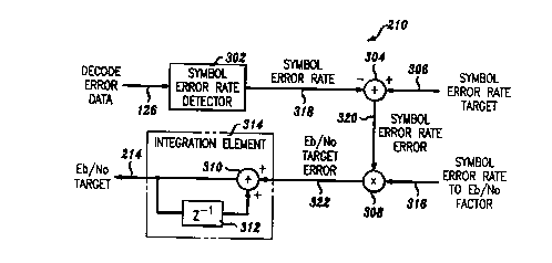
Figure 3 is a block diagram of a reverse outer loop power controller 210
utilizing symbol error detection in accordance with a preferred embodiment of
the
present invention. Reverse outer loop power controller 210 includes a symbol
error
rate detector 302, a summing node 304, a multiplier 308, and an integration
element
314. Integration element 314 includes a summing node 310 and a delay element
312.
Reverse outer loop controller 210 sets Eb/No target 214 for the inner control
loop described above with reference to Figure 2. Eb/No target 214 is increased
or
decreased to maintain a constant symbol error rate target 306.
Increasing/decreasing Eb/No target 214 will cause the inner control loop to
increase/decrease Eb 120 of reverse link transmitter 102 which will
decrease/increase the number of errors per symbol. In a preferred embodiment,
symbol error target 306 is a constant or parameter defined by the user. Symbol
error rate target 306 is chosen to minimize the power output of the mobile
station
while taking advantage of the error detection capabilities of the mobile
219971
telecommunication system. A typical symbol error rate target is in the range
of six
to twelve percent.
Symbol error rate detector 302 determines a symbol error rate 318 from
decode error data 126. Summing node 304 subtracts symbol error rate 318 from
symbol error rate target 306. The output of summing node 304, called symbol
error
rate error 320, is multiplied by a symbol error rate to Eb/No factor 316 via
multiplier 308. The output of multiplier 308, called Eb/No target error 322,
is
summed by integration element 314 to yield EblNo target 214. Integration
element
314 sums Eb/No target errors 322 by storing the previous sum in delay element
312
and adding the previous sum to Eb/No error target 322 via summing element 310.
Symbol error rate to Eb/No factor 316 is a constant value used to yield a
linear approximation of a non-linear relationship. The actual conversion
factor
should vary slightly depending on the value of Eb/No target 214. However,
multiplication by a constant value is done for purposes of simplicity and
provides
acceptable results. In an alternate embodiment, symbol error rate to Eb/No
factor
316 could be generated by using Eb/No target 214 to look up a value in a look-
up
table. In yet another embodiment, multiplier 308 could be eliminated, and
symbol
error rate error 320 and Eb/No target 214 could be used to look up an Eb/No
target
error 322 in a two-dimensional look-up table.
Another preferred embodiment of reverse outer loop power controller 210
utilizes both frame error rate detection and symbol error rate detection to
determine
Eb/No target 214. In this embodiment, the symbol error rate target is adjusted
according to a constant frame error rate. The actual power output level of the
mobile unit is still determined from the symbol error rate. However, instead
of a
constant symbol error rate target, as shown in Figure 3, the symbol error rate
target
is adjusted to maintain a constant frame error rate. This embodiment provides
the
tight power control which results from using symbol error rate detection, but
does
not require knowledge of the desired symbol error rate target to obtain a
given
frame error rate. This embodiment also corrects for different relationships
between
CA 02159971 1999-O1-OS
_g_
symbol error rate and frame error rate which may occur with differing radio
frequency
propagation conditions.
Figure 4 is a block diagram of one embodiment of reverse outer loop power
controller 210 utilizing symbol error rate detection and frame error rate
detection in
accordance with a preferred embodiment of the present invention. This
embodiment of
reverse outer loop power controller 210 includes a frame error rate detector
402, a
symbol error rate detector 404, a summing node 406, a multiplier 408, an
integration
element 410, a summing node 416, a multiplier 418, and an integration element
420.
Frame error rate detector 402 determines frame error rate 412 from decode
error
data 126. Summing element 406 subtracts frame error rate 412 from a frame
error rate
target 436. The output of summing node 406, called frame error rate error 426,
is
multiplied by a frame error rate to symbol error rate factor 422. The output
of
multiplier 408, called symbol error rate target error 428, is integrated by
integration
element 410. The output of integration element 410 is symbol error rate target
430.
1 S Symbol error rate detector 404 determines a symbol error rate 414 from
decode
error data 126. Summing node 416 subtracts symbol error rate 414 from symbol
error
rate target 430. The output of summing node 416, called symbol error rate
error 432, is
multiplied by symbol error rate to Eb/No adjustment factor 424 via multiplier
418. The
output of multiplier 418, called Eb/No target error 434, is integrated by
integration
element 420. The output of integration element 420 is Eb/No target 214.
Alternately, the symbol error rate target can be adj usted by using frame
error
rate sequential adjustment. Sequential adjustment based on frame error rate is
described
in U.S. Patent No. 5,257,283 to Gilhousen et al. In this embodiment, the
symbol error
rate target is varied each frame based on whether a frame error was detected.
If a
frame error is detected, the frame error rate target is multiplied by a
scaling factor and
subtracted from the previous symbol error rate
~159~'~1
-9-
target. If frame error is not detected, the difference of unity and the frame
error
rate target is multiplied by a scaling factor and added to the previous symbol
error
rate target.
While this invention has been particularly shown and described with
reference to several preferred embodiments thereof, it will be understood by
those
skilled in the art that various changes in form and details may be made
therein
without departing from the scope and spirit of the invention as defined in the
appended claims. For example, it will be understood that similar symbol error
based power control systems can be used in Time Division Multiple Access
(TDMA) and other systems employing digital modulation. Additionally, it would
be apparent that similar symbol based power control systems can be used in
forward (downlink) or reverse (uplink) telecommunication links.