Note: Descriptions are shown in the official language in which they were submitted.
2 1 ~ 7
~ETHOD AND APPARATUS FOR REDUCTION
OF ~IGHT INTEN8IT~ DECAY IN OPTICAL PUMPING DEVICES
Field of the Invention
The present invention relates to optical pumping
devices, such as atomic frequency standards,
magnetometers and the like, and particularly to atomic
frequency standards that generate and use light for
optical pumping and/or detection of atomic transition.
More particularly, the invention relates to methods
and apparatus for reducing the decay of light
intensity occurring over time with such apparatus.
Bac~ground of the Invention
In certain types of atomic frequency standards
and magnetometers, light is generated and used, for
example, for optical pumping and for detecting an
atomic (e.g., clock) transition. In such atomic
frequency standards and magnetometers, the stability
of the light intensity over long periods of time (many
years) is desired in order to maintain the integrity
of the standard or magnetometer.
An atomic frequency standard is a device that
uses an atomic transition frequency derived from an
atomic or molecular species experiencing a transition
between two or more well-defined energy levels of the
atom or molecule to control a standard frequency
oscillator.
For example, the two lowest energy levels of the
rubidium atom (Rb) are known as the ground state
hyperfine energy levels A and B. When atoms of
gaseous Rb-87 are interrogated (irradiated) with
microwave energy at a precise "transition frequency",
corresponding to the rubidium frequency that causes
atom transitions between the hyperfine energy levels A
21~01~7
and B, the rubidium atoms at hyperfine energy level A
will make the transition to level B, and vice versa.
The transition is employed as a highly accurate
frequency reference to which the frequency of a quartz
crystal oscillator or voltage-controlled crystal
oscillator (VCX0) can be electronically locked in
creating an atomic frequency standard.
For example, in atomic frequency standards the
frequency of a controllable frequency source, such as
a quartæ crystal oscillator, is controlled by means of
a physics package and associated electronics that are
devoted to maintaining the assigned output frequency,
typically 5 MHz or 10 MHz, on a very long-term,
exceedingly accurate and stable basis. By properly
slaving the quartz crystal oscillator to the frequency
of the atomic transition in the physics package, the
tendency of the quartz crystal to exhibit drifting due
to aging and other inherent as well as environmental
effects is markedly suppressed. The physics package
of a typical, passive, gas-cell, atomic frequency
standard generally includes a microwave cavity
resonator, an isotopic filter cell, an absorption
cell, a light source, a photodetector, temperature
control means, at least one magnetic shield
surrounding these components, and a C-field coil.
In a typical rubidium atomic frequency standard,
the light source 11 is a glass bulb containing
rubidium atoms which produces light by an rf-excited
plasma discharge. The rubidium in the lamp is heated
to a vapor state, approximately 110 C., and is
subjected to a high-energy rf field from an exciter
coil surrounding the glass bulb, thereby generating
light from the excited rubidium atoms. As shown
diagrammatically in Fig. 1, the "rubidium light" is
directed through a filter cell 25a which contains an
~ 2 ~ 7
isotope of rubidium, such as Rb-85, which filters out
light with a wavelength that will stimulate transition
of atoms from the hyperfine energy level B to any
optically-excited level C. The filtered rubidium
light is then directed through an absorption cell 25,
also called a resonance cell. The absorption cell 25
includes another isotope of rubidium, Rb-87, and the
filtered light energy absorbed by the Rb-87 atoms at
hyperfine energy level A causes a transition of the
Rb-87 atoms from level A to any optically-excited
energy level C. The atoms excited to energy level C,
however, do not remain at level C for more than tens
of nanoseconds, but return to ground state hyperfine
levels A and B in approximately equal numbers by
either spontaneous emission of light and/or by
collisions, including collisions with other atoms,
molecules, or the walls of the absorption cell 2S.
Since the filtered light does not allow transitions of
atoms from level B to level C, the continuing cycle of
optical excitation of atoms from level A to level C
and the redistribution of atoms falling from level C
between levels A and B eventually results in few, if
any, atoms at level A for excitation to level C, and
little or no absorption of the light passing through
the absorption cell 25 because the atoms have
accumulated at hyperfine energy level B. The atoms at
level A are said to have been "optically pumped" to
level B. If, however, microwave energy is applied to
the absorption cell 25 at the rubidium transition
frequency, transitions of atoms between hyperfine
levels A and B occur, re-introducing ato~.s at level A
which again absorb light energy and undergo a
subsequent transition to level C and thereby reduce
the light passing through the absorption cell 25.
~ 2 ~ 8 ~
The rubidium light passing through the absorption
cell 25 is incident on a photodetector 16, which
produces a current output which is proportional to the
intensity of the incident light. In a frequency-
locked loop, current output is processed by servo
electronics to provide a control voltage to a voltage
controlled crystal oscillator (VCXO) whose output is
multiplied (and synthesized) to the rubidium
transition frequency and provides the microwave energy
used to cause the transitions between hyperfine levels
A and B. When the frequency of the microwave energy
corresponds to the hyperfine transition frequency,
about 6.834 GHz for Rb-87, maximum light absorption
occurs and the current output of the photodetector 16
is reduced. If, however, the frequency of the
microwave energy does not correspond to the hyperfine
frequency, then more light will pass through the
absorption cell 25 to the photodetector 16, which in
turn increases its current output. Thus, the
photodetector current output can be used to provide an
error signal to maintain the output frequency of the
VCXO, typically 5 or lo MHz, (which, as noted above,
is multiplied and synthesized to produce the hyperfine
transition frequency of the rubidium atoms), thereby
creating an extremely stable 5 or 10 MHz output
frequency standard.
For years, the inventors have known that the
intensity of the light reaching the photodetector
decays slowly over time, and thereby degrades the
performance of the frequency standard. For example,
as previously discussed, in a typical frequency
standard, the light is eventually detected by a
photodetector, which produces a photocurrent that is
proportional to the intensity of the incident light.
Since an ac detection scheme is used in these devices,
~ 2~Q187
the signal information appears as a very small
modulated (ac) component (fundamental) of the total
photocurrent which has the property that it is zero
when the dc photocurrent is a minimum. The modulated
photocurrent is processed electronically by a
frequency-locked loop to produce an error signal which
is used to steer the VCXO, keeping it on frequency:
when the VCXO is on frequency the light reaching the
photodetector is a minimum and in this case the ac
component (fundamental) of the photocurrent disappears
so that there is no error signal. If the VCXo
frequency drifts, then the photocurrent is no longer a
minimum and an ac signal and associated error signal
results.
For example, if the VCXO frequency drifts away
from the nominal stabilized value by a certain amount,
this will produce an ac signal. The larger this
signal is, the larger the frequency-locked loop gain
and the better the loop can lock the VcXo frequency to
the hyperfine frequency. Generally, the greater the
intensity of the rubidium light, the larger is this ac
signal. Thus, it is advantageous to have high light
intensity. Since the photocurrent is electronically
converted to a proportional voltage (the "light
voltage"), a high light voltage is likewise
advantageous; any decrease in the light voltage
(corresponding to a decrease in light intensity) tends
to reduce the gain of the frequency-locked loop and
worsens the standard's frequency stability.
The intensity of the light that excites the
absorption cell is also an important factor in
determining the sensitivity and frequency
discrimination function of the physics package. As
the intensity of light at the photodetector decays,
the number of atoms undergoing transition as a result
~ 18 ~
of interrogation decreases with time, the light
voltage from the photodetector decays, the gain of the
frequency-locked loop decreases, and the performance
of the frequency standard degrades. As the loop gain
of the fre~uency-locked loop decreases further,
offsets will begin to appear and the short-term
frequency stability begins to worsen. Light voltage
decay can also produce frequency shifts of the
standard's output frequency due to the light shift
effect that maps light intensity changes into
frequency changes, resulting in frequency aging.
Some rubidium frequency standards are designed to
increase their internal supply voltage to a high value
prior to lamp ignition (this facilitates lamp
ignition). After lamp ignition the supply voltage is
reduced to its normal operating value by an electronic
switch that is activated by the light voltage. If,
for some reason, the light voltage falls below the
value at which switching occurs (threshold value), the
supply voltage will return to the higher value.
Should the light voltage decay during normal operation
so that it falls below the threshold value, the supply
voltage w;ill suddenly switch to the higher value and
remain there. This will produce a major change in the
unit's output frequency and render it unsuitable for
its intended purpose.
Even a small decay rate in the light intensity
can be a problem if it continues over a long period of
time. For example, a theoretical exponential decay at
a rate of 1 percent per month will cause the light
voltage to decay to 50 percent of its initial value
over a period of approximately six years, and a decay
rate of .6 percent per month will cause the light
voltage to decay to 50 percent of its initial value
over a period of about 10 years.
-
~ 2 ~ 8 7
The inventors have known and studied the problem
of light intensity decay for years. The rate of light
decay and the lower light intensity that is ultimately
reached has been found to vary widely and
unpredictably from apparatus to a~paratus. Testing
has indicated that in some groups of atomic frequency
standards as little as 6 to 10 percent of the initial
light intensity will ultimately be lost and in other
groups of atomic frequency standards as much as 40 to
50 percent of the initial light intensity will
ultimately be lost. Testing has also indicated that
the rate of loss varies from group to group, with the
time constant of an equivalent exponential decay being
as low as 1 to 2 months with some groups and as high
as 3 to 6 months in others. Many possible causes of
the light decay were considered and investigated, but
the primary cause of the light decay remained unknown
until recently. Thus, this unpredictable loss of
light intensity has continued to degrade the
performance for many atomic frequency standards, and a
method and apparatus that can reduce light intensity
decay is needed to obtain predictable aging and
su~stantially improve the performance of optical
pumping devices, such as atomic frequency standards,
magnetometers and the like.
~ummary of the Invention
The inventors have now discovered that the time
decay of light intensity is due primarily to the
decreasing reflectivity of reflec~ing surfaces within
the physics package. In a frequency standard, the
light, once generated, reflects off internal surfaces
of the physics package, and such reflected light is a
significant percentage of the total useful light
reaching the absorption cell. The exciter coil
~ 2~ 6~ ~7
surrounding the glass bulb is advantageously made of
silver, which is selected as much for its reflectivity
as for its electrical conductivity. Other surfaces,
such as the interior surfaces of a resonance cavity
surrounding the absorption cell, are silver plated to
provide additional reflected light. The inventors
have discovered that the tarnishing and oxidation over
time of the useful light reflecting surfaces is the
principal cause of the time decay of light intensity
and that by passivating the light reflecting surfaces
of the device, especially the surfaces of the exciter
coil, light intensity decay problems can be
substantially eliminated. Such tarnishing may be the
result of, or accelerated by, the outgassing of
physics package materials.
According to the present invention, surfaces that
reflect optical pumping light are passivated so their
light reflectivity does not change over time. Such
reflecting surfaces can be "passivated" in various
ways. In embodiments of the invention, the
passivating step can include the step of providing the
surfaces with a non-reflective layer, or the step of
providing the surfaces with a layer whose reflectivity
remains substantially constant over time, or the step
of altering the surfaces so their reflectivity does
not change over time. Examples of passivation include
forming a stable light reflective layer on such
surfaces by gold plating, sulfides, oxides and the
like. Thus, a method for reducing light intensity
decay in an atomic frequency standard that uses an
ensemble of atoms that are optically pumped and
interrogated by a microwave signal so as to produce a
photocurrent which is used to control the frequency of
the microwave signal, includes the steps of:
providing a plasma discharge lamp for optically
2:~6~187
pumping the ensemble of atoms, and providing surfaces,
or passivating the surfaces, that reflect light from
the lamp toward the ensemble of atoms so their light
reflectivity does not change over time.
In a frequency standard that includes a light
source, an absorption cell, a photodetector for
detecting the light from the light source, and an
exciter coil positioned to excite the light source to
stimulate emission of the light, and including a
surface to reflect a portion of the light toward the
absorption cell and photodetector, the reflective
surface of the exciter coil is passivated to reduce
decay of the light intensity, over time, of the light
available at the photodetector. Where the light
source comprises a lamp assembly including a light
reflective surface, the reflective surface of the lamp
assembly is passivated. In one embodiment of the
invention, the passivated light reflective surface
comprises gold. In another embodiment, the exciter
coil surrounds the lamp and the lamp's passivated
surface comprises gold.
By providing passivated reflective surfaces whose
reflectivity does not change with time, the present
invention substantially reduces the unwanted effects
associated with the light intensity decay over time.
Additional objects, features, and advantages of
the invention will become apparent to those skilled in
the art upon consideration of the following detailed
description of a preferred embodiment exemplifying the
best mode of carrying out the invention as presently
perceived.
Brief Description of the Drawinq~
Fig. 1 is a diagrammatic representation of an
optical physics package;
: 2~ ~0~87
Fig. 2 is a side sectional view of the optical
physics package along with the associated electrical
components shown schematically;
Fig. 3 is a graph of reflectance versus coating
thickness of Ag2S; and
Fig. 4 shows a lamp housing with a lamp holder
and exciter coil.
~etaile~ DescriPtion of the Drawings
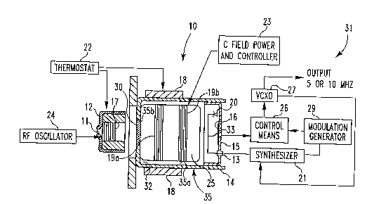
The exemplary embodiment of the optical-physics
package 10 illustrated in Fig. 2, is directed to an
embodiment using one of the alkali metals, viz.,
rubidium. The embodiment includes an electrodeless
gas discharge lamp 11, which is evacuated and filled
with rubidium, plus a suitable buffer gas at a
pressure, generally about 2 torr (0.27 kPa),
surrounded by an exciter coil 17. In conventional,
commercial atomic frequency standards of the type most
commonly used, the exciter coil 17 is typically formed
by separated turns of uncoated silver wire. The coil
17 is activated by a radio-frequency oscillator 24.
The lamp 11 within a lamp housing 12 of the optical-
physics p;ackage 10 is arranged with a thermostat 22
which renders a controllable temperature, usually
about 110 C., which is re~uired for generating the
requisite rubidium vapor pressure in the lamp 11. As
can be appreciated, the thermostat 22 keeps the
temperature of the liquid rubidium metal constant
within narrow limits, as the light emitted by the lamp
11 is dependent on variations in the rubidium vapor
pressure and, hence, on this temperature.
The light radiated from the lamp 11 and reflected
from exciter coil 17 and other small surfaces arrives
at a photodetector 16 after transversing an absorption
cell 25 positioned between lamp 11 and photodetector
--10--
~16018~
16. The light reaching the photodetector is a
combination of direct path light from the lamp 11 and
light reflected from light reflective surfaces of the
exciter coil 17, the lamp housing 12, and microwave
resonant cavity 35. The absorption cell 25 comprises
an evacuated cylindrical glass bulb which is likewise
filled with vaporized rubidium having a suitable vapor
pressure and with a buffer gas, such as nitrogen or
argon, or some mixture of such buffer gases.
In the particular embodiment of the optical-
physics package 10 shown in Fig. 2, it should be
observed that no separate filter cell is employed as
is often conventional in such devices, but instead an
absorption cell 25 of special design as that described
in U.S. Patent No. 3,903,481 to Ernest Jechart is
contemplated. Thus, the absorption cell 25 is one
containing an isotopic mixture and, more particularly,
a mixture of Rb85 and Rb87 atoms in accordance with
the teaching of said patent to Jechart.
When the Rb87 in the lamp 11 is excited it emits
light having a spectrum containiny the two strong
optical lines of Rb87 (Dl at 794.8 nm and D2 at 780.0
nm) each of which, in turn, contains two main
hyperfine components. A beam of such light
transversing the absorption cell 25 containing the
buffer gas as well as the mixture of Rb85 and Rb87
isotopes causes the preferential absorption of one of
the hyperfine components for both Dl and D2 lines. The
remaining Dl and D2 spectral component serves as
optical pumping light and brings about a population
inversion between the two ground state hyperfine
levels of Rb87 in the absorption cell 25.
Preferentially, only those atoms that are in the lower
hyperfine state absorb the optical pumping light and
are raised into optically-excited high-energy states.
--11--
~ 216~187
Furthermore, by spontaneous emission or
collision, such atoms return to one of the ground
hyperfine states. Because the number of atoms able to
absorb the optical pumping light decreases, the
absorption cell 25 tends to become transparent. Upon
introduction of microwave radiation into the microwave
cavity 35, resonant at a frequency of 6.834...GHz
corresponding to the energy gap between the two ground
state hyperfine levels, the population increase of
atoms in the lower hyperfine level increases. The
increase in population provides more atoms for the
absorption of light from the light source. The atoms
that arrive in this lower state are, of course,
optically pumped and raised to higher energy states.
As the atoms drop into the lower ground state
hyperfine level from the upper ground state hyperfine
levels, a correspondingly smaller amount of light
reaches the photodetector 16 since light is being
actively absorbed by Rb87. When there is less light
reaching the photodetector 16 there is a corresponding
reductiorl in the photocurrent produced by the
photodetector 16. This decreasing light signal, as
the micro;wave frequency approaches the very-sharply-
defined rubidium frequency, is converted
electronically to an error signal with amplitude and
phase information that is used to steer the VCXO 27
via its control voltage to keep it at a standard
frequency of e.g., 10 MHz. When the microwave
frequency is equal to the rubidium transition
frequency, VCXO 27 is frequency locked to the stable
atomic transition frequency. Thus, by use of the
above described scheme the VCXO 27 can be exactly 10
MHz when the microwave frequency is exactly equal to
the frequency of the rubidium transition.
-12-
~160187
It is to be noted that the photodetector 16 and
absorption cell 25 are fully enclosed within the
microwave cavity resonator 35 which is of cylindrical
design and includes a cylindrical body 14 having a
light-permeable dielectric window 30 therein and a lid
15 integrally connected to said body 14 to thereby
fully seal the same. It has been found most
advantageous to construct the cavity resonator 35 from
a material having high magnetic permeability in low
magnetic fields. It can be seen that the cavity
resonator 35 is closed to the outer air and thus may,
when connected to a heater ring 18, be advantageously
controlled to maintain by heat control means 22 a
constant temperature, e.g. 75 C. In one embodiment,
the material of the cavity resonator 35 may comprise a
nickel-steel alloy containing about 17 to about 20
percent iron, about 5 percent copper and low
percentages of manganese or chromium. In general,
however, any of a host of ferromagne~ic compositions
or materials capable o~ rendering equivalent magnetic-
permeable properties such as metals or alloys of high
magnetic permeability may serve as the resonant cavity
35 as long as such permeability is at least equal to
if not significantly greater than that of pure iron
with or without additional constituents, such as
cobalt and chromium. Such metals, as known, provide
effective shielding from the earth's magnetic field
and from any other magnetic field or fields which
might cause interference in order to achieve the
desired precise control of the resonant frequency of
operation.
In conventional atomic frequency standards, the
resonator cavity 35 is generally silver plated, or
copper flashed at first and thereafter silver plated.
Thus, the light reaching the photodetector also
~ 1 8 7
includes light reflecting from the interior walls of
the resonator cavity 35.
A current supplied to the windings 19 cause a
magnetic field known as a "C-fieid" to be established.
A number of C-field windings 19 are made around the
inside wall of the microwave cavity resonator and,
hence, around the absorption cell 25. Thus, the
windings 19 are disposed inside the cavity resonator
35 for producing, by means of a C-field power and
controller 23, a dc magnetic field of a predetermined
intensity. Generally, this could vary over a wide
range but is usually between about 0 to about 1 gauss.
Although any number of wound sections may be used, two
separately energizable sections may be readily
utilized as shown, l9a and l9b. One of the functions
of the C-field windings 19 is to create in operation a
magnetic bias field in the microwave cavity resonator
35 and, therefore, within the absorption cell 25. The
coils l9a and l9b may be wound around the outside of
the absorption cell 25 and any separation or space 32
between the absorption cell 25 and said cavity
resonator 35 may be readily filled with a non-magnetic
polymer ~aterial such as polymeric silicone elastomers
including room temperature-vulcanizing silicone rubber
compounds, organosiloxane polymers and the like.
Generally, the windings 19 consist of a single layer
of turns of insulated copper wire. The C-field
windings 19 are placed in an appropriate position to
create typically a predetermined magnetic field not
exceeding approximately one gauss to bias magnetically
the absorption cell 25 and thereby to separate the
zeeman levels of each hyperfine state of the vapor
atoms. Connected through the wall of lid 15 is a
microwave input means comprising a feed-through
capacitor 13 coupled to a step recovery diode 20 by
-14-
-
means of a conductor 33. By such input means
microwave energy is rendered to the interior of the
cavity resonator 35 to provide microwave coupling
thereto.
As previously discussed, the microwave cavity
resonator 35 is excited with microwave energy at the
atomic resonance frequency of the atomic vapor within
the absorption cell 25 and in the case of rubidium at
a frequency of 6.834...GHz. In practice, this signal
is derived from the 10 MHz VCX0 27 by means of a
frequency synthesizer 21 and modulation generator 29.
Thus, the microwave energy applied to the cavity
resonator 35 is frequency modulated at a low
modulation frequency, generally about 150 hertz. The
output of the synthesizer 21, which iS generally about
60 MHz plus an additional signal of 5.3125 MHz is
applied to a microwave generating means including the
feed-through capacitor 13, the step recovery diode 20
and the length of the conductor 33. As is known, the
step recovery diode 20 ~unctions as a harmonic
generator and mixer producing an output signal that
contains multiple harmonics of the input signal, the
one hundr;ed fourteenth harmonic of the input 60 MHz
frequency being 6.84 GHz. Additionally, the diode 20
functions as a mixer to provide microwave energy at a
frequency of 6834.6875 MHz (6840.0000 MHz-5.3125 MHz),
the frequency of Rb87 in one preferred embodiment. As
already discussed, the injection of electromagnetic
energy at this frequency interacts with the rubidium
absorption cell 25 to produce a detectable partial
reversal of the optical pumping process.
An error signal is generated to control VCXO 27
by the following scheme. The ac signal from the
photodetector 16 is coupled to an amplifier located in
control means 26 and the amplified signal is applied
-15-
216 0~ ~'7
to a synchronous demodulator in control means 26 which
also receives a signal from a modulation generator 29.
By this means it can be determined if the carrier
frequency of the signal applied to the cavity
resonator 35 is properly centered on the frequency of
the hyperfine transition 6.834...GHz. Any deviation
or displacement results in an error signal at the
output of the demodulator of control means 26. This
signal is used to control the VCXO 27 which may be
modified so as to maintain the frequency of the
synthesized microwave signal at 6.834...GHz centered
on the frequency of the hyperfine transition of
rubidium.
The above discussion relates to a conventional
physics package 10. Thus, such a physics package 10
described is subject to the same light intensity decay
problem experienced by all conventional physics
packages.
The inventors have discovered that the decay of
light intensity is caused primarily by the decreasing
reflectivity of such light reflecting surfaces as the
coils of wire in exciter coil 17, the light reflective
portions of lamp housing 12, the edges 35b of
microwave; cavity resonator 35 that are adjacent the
dielectric window 30, and the interior surfaces 35a of
the microwave cavity resonator 35. Some of these
surfaces are silver or silver plate and it has been
determined that the time dependent tarnishing and
oxidation of such silver surfaces is a principal cause
of the time decay of light intensity at the absorption
cell 25. Such loss of bright intensity decreases the
sensitivity and frequency discrimination ability of
physics package 10, as described above.
However, improvements according to the present
invention, if made to a conventional physics package,
-16-
2 1 ~ 7
will dramatically reduce the decay in light intensity
and thereby improve the long term stability of the
associated frequency standard, magnetometer, or the
like.
For example, the reflective surfaces of the
physics package, such as the surfaces of the exciter
coil 17 surrounding the discharge lamp, can be coated
(tarnished) with silver sulfide (Ag2S).
Typically, the exciter coil 7 is made from
silver, and is therefore subject to tarnish in the
normal course of events due to exposure to atmosphere,
and possible outgassing of adhesives, etc. in the
standard, particularly as it operates at elevated
temperature. The optical constants for tarnish on
silver have been measured and can be used to compute
the light reflectivity for silver wire as a function
of tarnish. The calculation shows that the reflected
light decreases rapidly at first and then levels off
for tarnish thickness above some threshold value.
Thus, for a layer of tarnish thicker than the
threshold value, there should be no further light
decay due to the tarnished wire, even if the tarnish
layer increases while the lamp is operating in a unit.
Moreover, the pre-tarnish layer does not have to be
precisely controlled - only made greater than the
threshold level.
As shown in Fig. 3, a .4 ~m (micron) Ag2S coating
formed on a silver substrate results in a reflectance
that remains essentially constant at about 0.25. Any
additional tarnish that forms on the reflective
surface beyond the .4 ~m coating will not produce any
significant decrease in the reflectivity. Thus, by
initially coating the reflective surfaces with at
least a .4 ~m coating of Ag2S, the physics package can
~ 216~l8~
be artificially "aged", and thereafter experience only
insubstantial light intensity decay.
Another advantage of using tarnish is that it
forms a coating on the silver wire that is stable over
long periods of time (many years) at the elevated
operating temperatures of the lamp coil. This is
inferred from the observation that tarnish forms
naturally on initially untarnished coils during normal
operation, and field experience shows that it is
stable (indefinitely). Other coatings, such as paint,
epoxies and materials requiring organic binders, may
peel, flake or undergo other types of undesirable
physical or chemical transformation at the required
operating temperatures in the presence of rf energy.
Such behavior is hard to predict in advance because of
the requirement of stability over long time periods of
many years.
Yet another advantage of using tarnish on the
silver lamp coil is that it preserves the ignition
properties of the lamp coil. From the perspective of
rapid lamp ignition, silver is an ideal material for
the lamp coil wire because of its extremely lower rf
surface resistivity (which, in turn, is due to its
very smali skin depth at rf frequencies). Plating
silver with even a very thin layer of some other metal
(e.g., tin or nickel) can seriously degrade the
ignition properties of a lamp coil. When tarnish is
used on a silver coil the ignition properties
characteristic of untarnished silver appear to be
retained. This is reasonable because tarnish, being a
semiconductor, should be invisible to rf fields when
the coating is very thin.
One method of pre-tarnishing silver that works
well is to use a large container, such as a glass
beaker, with powdered sulfur in the bottom.
-18-
.,
216~187
Components with light reflective silver surfaces, such
as lamp exciter coils wound into coil forms with solid
silver wire (or the silver wire from which such coils
are wound) the lamp housing 12, and the cavity
resonator 35, can be placed inside the container on
top of a stainless steel screen. The container can
then be closed, and heated, for example, by placing it -
on a hot plate. When the heated container is left on
the hot plate for four or more hours (overnight works
well~, the silver surfaces turn black which is the
color of Ag2S.
Two lamp exciter coils were pre-tarnished in this
way and tested. The tests were carried out using four
rubidium frequency standard units that had been
operating for a total of about five months. These
were units that originally had very high light voltage
decay rates, i.e., >10% per month. At the end of the
five months, the original lamp coils of these units
were removed and two were replaced with pre-tarnished
lamp coils, one with light tarnish, and one with heavy
tarnish. The other two were replaced with new,
untarnished (shiny) lamp coils. The four units were
then placed back in test and the light voltage
recorded for 50 days. The light voltage decay rate
for the untarnished coils averaged 2.6 percent per
month. The average decay rate for the pre-tarnished
coils was .54 percent per month, a significant
improvement. A second set of similar experiments were
carried out for about one month right after the first
set. In these experiments, the light voltage decay
rate for the untarnished coils averaged 5.1 percent
per month. The average decay rate for the pre-
tarnished coils was 1.1 percent per month, again a
significant improvement.
21~0187
Of course, the tarnish layer reduces the light
incident on the photodetector. However, this effect
can be offset by other means, such as an increase in
the amplification of the photocurrent or an increase
in the lamp operating temperature. With appropriate
compensation to minimize the effect of the reduced
reflectance, the improved physics package will provide
a stable light intensity over a long period of time
and thereby maintain the integrity of the standard or
magnetometer. Thus, the present invention provides a
greatly improved physics package by dramatically
reducing the light intensity decay.
Of course, it will be appreciated that
passivation methods can be applied to other metals
that are sometimes used, such as copper or aluminum.
Moreover, pre-tarnishing the metals is not the only
way of passivating the metals. For example, the
reflective surfaces can be covered with a material
that is non-reflective, or a coating whose
reflectivity does not change with time, or a
transparent coating that prevents tarnishing or
oxidation. In addition, light reflective surfaces of
the physi;cs package can be plated with a metal that
does not tarnish or oxidize, such as gold. "Chrome"
may also be used where its magnetic properties will
not interfere with operation of the physics package.
In a preferred embodiment, silver wire is plated
with gold. Gold-plated silver wire has been found to
have excellent lamp ignition properties, almost as
good as unplated silver wire. This can be attributed
to the fact that the ac surface resistivity of gold is
only 16 percent greater than that of silver. Use of
gold plating suffers from the disadvantage that the
silver "base" metal can diffuse through the gold
plating over a period of time and then possibly
-20-
,,
~601~7
tarnish on the surface. However, the inventors have
discovexed that the majority of tarnishing occurs
early on in the life of the device and then slows
down. Thus, the tarnishing is believed to be caused
by some transient phenomenon, possibly the outgassing
of materials used in the construction of the physics
package. Therefore, the gold plating only has to
protect the surface until the transient phenomenon is
over, at which time diffusion of the silver through
the gold plating will have little effect since the
tarnishing agent in the atmosphere will have been
depleted.
A preferred embodiment, shown in Fig. 4, includes
a lamp housing 12 having an interior cavity 12a for
receiving a gas lamp bulb 11, a lamp holder 13, and an
exciter coil 17. The lamp holder 13 includes a
generally hemispherical or parabolic lamp receiving
surface 13a configured to mate with a lamp bulb 11.
Preferably both the exciter coil 17 and the lamp
receiving surface 13a are gold-plated so as to
~ xi~;ze the amount of reflective surface in the
interior cavity 12a.
Additionally, the reflective surfaces of the
cavity resonator 35 (Fig. 2) can be gold-plated. The
reflective surfaces can include the interior surface
35a and the edges 35b of the cavity resonator 35 that
are adjacent the dielectric window 30.
Although the invention has been described in
detail with reference to a certain preferred
embodiment, variations and modifications exist within
the scope and spirit of the invention as described and
defined in the following claims.