Note: Descriptions are shown in the official language in which they were submitted.
3 4 ~
FOUR OUADRANT CURRENT MODE SWITCHING AMPLIFIER
This invention relates to a four quadrant current
mode switching amplifier and is particularly concerned with
a switching topology which provides negative current mode
feedback in all four quadrants of operation.
Backaround of the Invention
A conventional high voltage linear amplifier
arrangement has two separate blocks, a high voltage power
supply converter (i.e. DC to DC) to provide high voltage DC
to power a linear amplifier, and a linear amplifier that
takes an analog reference input voltage and amplifies it by
a desired gain factor. The disadvantages with this
conventional arrangement are relatively high numbers and
size of components, power efficiency, cost and reliability.
Published European patent application 386,933
exemplifies a switching topology for a dc-to-ac converter.
The paper entitled "UPS System Employing High Frequency PWM
Techniques" (APEC '90 Fifth Annual IEEE applied power
electronics conference and exposition, 11-16 March 1990,
Los Angeles, CA; XP 000143314, pages 414-421, A.M. CAMPOS
et al.) illustrates further switching topologies relating
to other types of converters.
Summarv of the Invention
An object of the present invention is to provide an
improved four quadrant current mode switching amplifier.
In accordance with the present invention there is
provided a four quadrant current mode switching amplifier,
comprising an input terminal (10) for accepting an analog
input voltage; an output terminal (12) for providing an
amplified output voltage; a switching topology power
converter (20) having inputs for accepting a direct current
source of electrical energy (60, Ground) and having the
output terminal, the power converter further has electronic
switch means (24, 26, 28, 30) which are switchable for
regulating the output voltage and for changing operation of
the converter between the four quadrants; means for
generating a sign signal (72) in dependence upon the input
voltage; means for generating a slope signal (74) in
i-~
4 ~
l/2
dependence upon the input and output voltages; means for
generating an error voltage signal (76, 78) in dependence
upon the input and output voltages; means for sensing
current (32) in the switching topology power converter to
provide current mode feedback as the power converter
operates in any of the four quadrants; means for generating
a width modulated pulse (16), at a first frequency, in
dependence upon the error voltage signal and the sensed
current; and means for controlling (18) the electronic
o switch means in the switching topology power converter, at
a second frequency, which is lower than the first
frequency, for changing the quadrant in which the converter
operates, in dependence upon the width modulated pulse, the
sign signal and the slope signal, in order to regulate the
output voltage.
W094/~625 216 0 3 ~ ~ PCT/CA93/00235
In an embodiment of the present invention the
means for sensing current includes a current sensing
transformer.
An advantage of the present invention is providing
the equivalent response of a high voltage linear amplifier
with a switching converter topology. This reduces the
number and size of components needed thereby providing a
more efficient and reliable circuit, with lower cost and
power.
o Br;ef Descri~tion of the Drawinas
The present invention will be further understood
from the following description with reference to the
drawings in which:
Fig. 1 illustrates a functional block diagram of a
four quadrant current mode switching amplifier in
accordance with an embodiment of the present invention; and
Fig. 2 schematically illustrates detail of the
pulse width modulator and logic device of the four quadrant
current mode switching amplifier of Fig. 1.
Fig. 3 illustrates in plan view the current
sensing transformer;
Fig. 4 schematically illustrates the current
sensing transformer;
Fig. 5 illustrates in plan view the power
transformer; and
Fig. 6 schematically illustrates the power
transformer.
Similar references are used in different figures
to denote similar components.
Detailed Descri~tion
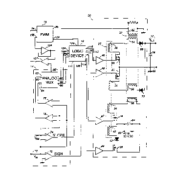
Referring to Fig. 1, there is illustrated, in a
block diagram, a four auadrant current mode switching
amplifier in accordance with an embodiment of the present
invention. The four quadrant current mode switching
amplifier includes an analog signal input 10, an amplified
signal output 12, an error voltage circuit 14, to which
both the input 10 and output 12 are connected, a pulse
W094/~625 2 16 0 ~ 4 ~ PCT/CA93/00235
width modulator (PWM) 16 coupled to the error voltage
circuit 14, a logic device 18 connected to the PWM 16, and
a switching topology 20, coupled to the logic device
18, and connected to the amplified signal output 12. The
switching topology 20 includes a power transformer 22, four
FET switches 24, 26, 28, and 30 and a current sensing
transformer 32. Conveniently, the FET switches 24, 26, 28,
and 30 are referred to as primary, load drain, positive
ground, and negative ground, respectively. The power
transformer 22 has a primary winding 34 and three secondary
windings 36, 38, and 40. The logic device 18 is connected
to the switching topology via buffers 42, 44, 46, and 48
and the gates of FET switches 24, 26, 28, and 30,
respectively. The current sensing transformer 32 has a
primary winding 52 and three secondary windings 54, 56, and
58. Conveniently, the secondary windings 54, 56, and 58
are referred to as positive current sense, negative current
sense and primary current sense, respectively.
On the power input side of the switching topology
20, battery power (-40 to -60 V) is applied between a
negative battery input 60 and ground. The primary FET
switch 24, power transformer primary winding 34 and the
primary current sense secondary winding 58 are series
connected between the negative battery input 60 and ground.
The power transformer secondary winding 40, diode 62 with
cathode side toward ground, and the load drain FET switch
26 are also series connected between the negative battery
input 60 and ground. The negative battery input 60 is
filtered to ground via a capacitor 64.
On the power output side of the switching topology
20, power output is provided between the amplified signal
output 12 and a return terminal 66 that is connected to
ground. The positive ground FET switch 28, the power
transformer secondary winding 36, the positive current
sense secondary winding 54, and a diode 68, with the
cathode side toward the output 12, are series connected
between the return terminal 66 and the amplified signal
W094/~625 21 6 0 3 4 0 PCT/CA93/00235
output 12. A diode 70, with the anode side toward the
output 12, the negative current sense secondary winding 56,
the power transformer secondary winding 38, and the
negative ground FET switch 30, are series connected between
the amplified signal output 12 and the return terminal 66.
The error voltage circuit 14 includes comparators
72 and 74, difference amplifiers 76 and 78, and an analog
MUX 80. The analog signal input 10 is connected to
noninverting inputs of comparator 72 and amplifier 76 and
lo inverting inputs of comparator 74 and amplifier 78. The
amplified signal output 12 is connected to noninverting
inputs of comparators 74 and amplifier 78 and the inverting
input of amplifier 76. The inverting input of comparator
72 is connected to ground. Outputs of comparators 72 and
74 are connected to the logic device 18 and provide sign
and slope signals, respectively. Outputs of amplifiers 76
and 78 are connected to the analog MUX 80 via inputs 82 and
84, respectively. The analog MUX 80 also has inputs 86,
88, and 90 connected to the logic device 18 for receiving
an enable signal, MUXEN, a synchronized sign signal, RSIGN,
and a synchronized slope signal, RSLOPE, respectively from
the logic device 18. The analog MUX has an output 92.
The PWM 16 has feedback and sense inputs 94 and
96, a reference voltage output 98 and a pulse output 100.
The analog MUX 80 is coupled to the PWM 16 via a amplifier
102, the output 92 being connected to the inverting input
of amplifier 102. The reference voltage output 98 is
connected to the noninverting input of amplifier 102 via a
voltage follower 104. The primary winding 52 of the
current sensing transformer 32 is connected to the sense
input 96 of PWM 16 to provide current mode feedback from
the switching topology 20.
The logic device 18 has a pulse input 106, sign
input 108 and slope input 110. The pulse output 100 of PWM
16 is connected to the pulse input 106 of the logic device
18. The sign and slope inputs 108 and 110 are connected to
the output of comparators 72 and 74, respectively. The
W094/28625 21 6 0 3 4 ~ PCT/CA93/00~
logic device 18 has drive outputs 112, 114, 116, and 118
connected to buffers 42, 44, 46, and 48, respectively. The
logic device 18 also has MUX enable, synchronized sign and
synchronized slope signal outputs 120, 122, and 124,
respectively, connected to the inputs 86, 88, and 90,
respectively, of MUX 80.
In operation, an amplified output signal VOUt, of
-200 to +200 V, is generated by taking the difference,
using amplifiers 76 and 78, between the analog input signal
0 Vin, of -45 to +45 V, and the output signal VOut to produce
an error signal Verror~ The analog MUX 80 selects the
positive VerrOr in dependence upon values of slope and sign
bits, referred to as SIGN and SLOPE, applied to inputs 88
and 90, respectively. The error signal VerrOr is then
subtracted from a reference voltage signal Vref, supplied by
output 98 of the PWM 16, using the amplifier 102, to form a
primary inductor current programming voltage Vfb used to
modulate the pulse width produced by the PWM 16.
The sign bit, SIGN, is derived from the analog
input signal Vin by comparing i-t to ground, to determine if
it is positive or negative, using the comparator 72. The
slope bit, SLOPE, iS derived by comparing the output signal
VOut to the input signal Vin, using comparator 74 to
determine if the output signal vOut should be raised or
lowered relative to the input signal Vin. The switching
topology 20 is changed dynamically to either source current
or sink current in dependence upon the sign and slope bits
supplied to the logic device 18 via inputs 108 and 110.
The logic device 18 also synchronizes the sign and slope
bits SIGN and SLOPE to provide synchronized sign and slope
bits, RSIGN and RSLOPE.
The switching topology 20 is operated as follows.
When the primary 34 of the power transformer 22 is
supplying energy to a load connected to the output 12 and
return terminal 66, the primary FET switch 24 is turned on
and one of the two output FET switches 28 (positive ground)
or 30 (negative ground) is turned on, depending upon the
W O 94128625 216 0 3 4 0 PCT/C A93100235
desired output polarity. When energy must be removed from
the load, the primary FET switch 24 is turned off and the
load drain FET switch 26 is turned on. The appropriate
output FET switch 28 or 30, is then used as the primary
switching device and is modulated by the PWM 16. Thus, the
load drain FET switch 26 becomes the energy dump path for
draining the load and returning the energy into the source
capacitor 64. Depending upon the state of the SIGN and
SLOPE bits, one of the three FET switches 24, 28 or 30 is
used as the modulated primary, thereby allowing the
switching topology 20 to source or sink current as
required, with either a positive or negative output
voltage, thus, providing four quadrant operation.
The current sensing transformer 32 provides
current feedback to the pulse width modulator 16 by having
a secondary winding in each of the three loops in which the
FET switch can act as the primary switching device
modulated by the PMW 16. That is, when the primary FET
switch 24 is turned on, the primary current sense secondary
winding 58 provides current mode feedback, via the primary
winding 52 of the current sensing transformer 32, to the
PWM 16.
When the primary FET switch 24 is turned off and
the positive ground FET switch 28 is turned on, the
positive current sense secondary winding 54 provides
current mode feedback to the PWM 16. Similarly, when the
primary FET switch 24 is turned off and the negative ground
FET switch 30 is turned on, the negative current sense
secondary winding 56 provides current mode feedback to the
PWM 16. This switching of feedback allows negative current
mode feedback in all four quadrants of operation.
Before describing in detail how this is
accomplished a description of the remaining inputs to and
outputs from the pulse width modulator 16 and the logic
device 18 is required.
Referring to Eig. 2, there is schematically
illustrated, detail of the pulse width modulator and logic
W094l28625 216 0 310 PCT/CA93/00235
device of the four quadrant current mode switching
amplifier of Fig. 1. The present embodiment of the four
quadrant current mode switching amplifier has additional
inputs not shown in Fig. 1 to simplify the description of
5 the circuit. The additional inputs, illustrated in Fig. 2,
are a power-up reset input 126, a remote shutdown input
128, an external clock input 130, a sample rate clock input
132, and an AC-DC mode select input 134.
In Fig. 2, the PWM 16 is provided by a SI9110
lo integrated circuit, by Siliconix. The SI9110 integrated
circuit used has a 14 pin package. The feedback and sense
inputs 94 and 96, a reference voltage output 98 and a pulse
output 100 of PWM 16 are provided by SI9110 pins 14, 3, 10,
and 4, respectively. The external clock input 130 is
connected to an oscillator input 136 (SI9110, pin 8). The
remote shutdown input 128 is connected to a shutdown input
138 (SI9110, pin 11).
In Fig. 2, the logic device 18 is provided by a
programmable array logic, specifically an AMD 26V12 PAL by
Advanced Micro Devices. The AMD 26V12 PAL used has a 28
pin package. The pulse input 106, sign input 108 and slope
input 110 are provided by AMD 26V12 PAL pins 2, 3, and 8,
respectively. The power-up reset input 126 is connected to
an input 140 (AMD 26V12, pin 6). The external clock input
130 is connected to an input 142 (AMD 26V12, pin 1). The
sample clock input 132 is connected to input 144 (AMD
26V12, pin 4). The AC-DC mode select input 134 is
connected to an input 146 (AMD 26V12, pin 5~. The remote
shutdown input 128 is connected to an input 148 (AMD 26V12,
pin 9). Details of the ADM 26V12 PAL input and outputs and
A the boolean equations that describe its internal logic are
summarized in Table A.
WO94/~625 216 0 3 4 0 PCT/CA93/00235
NAME PIN DESCRIPTION
INPUTS
SYNC pin 1 480 kHz sync clock input
PWM pin 2 pulse width modulator input
5 SIGNIN pin 3 asynchronous sign bit input
SMPCLK pin 4 low frequency (60kHz) sample
C1OCk
AC_DC pin 5 ac or dc mode select
RESET pin 6 master reset line (turns off all
FETS)
SLOPEIN pin 8 asynchronous slope bit input
SHTDWN pin 9 shutdown input to PAL
TRISTATE pin 28 testability tristate pin
15 OU1~U1S
PRIMFET pin 15 primary FET drive output
LOADDRAIN pin 16 load drain drive output
NEGGND pin 17 negative ground drive output
POSGND pin 18 positive ground drive output
20 MUXEN pin 19 mux enable
RSIGN pin 20 synchronized sign bit
RSLOPE pin 22 synchronized slope bit
H, L, X, Z = 1, 0, .X.,.Z.;
equations
assign clocks
[RSIGN.C,RSLOPE.C]=SMPCLK;
logic definitions: boolean equation definition
! = logical inversion
# = logical or
$ = logical exclusive or
& = logical and
H = logical 1
L = logical 0
X = don~t care
Z = tristate
RSIGN:=SIGNIN;
RSLOPE:=(!AC_DC ~ SLOPEIN) # (AC_ DC ~ SIGNIN);
CA 02160340 1998-0~-20
PRIMFET=! (!SHTDWN & RESET & ((AC_DC & PWM)
# (PWM & !AC_DC & !(RSIGN $ RESLOPE))));
LOADDRAIN=! (!SHTDWN & RESET & ((!AC_DC & !RSIGN & RSLOPE)
# (!AC_DC & RSIGN & !RSLOPE)));
NEGGND=!(!SHTDWN & RESET &
((!AC_DC & RSIGN & !RSLOPE & PWM)
' # (!RSIGN & !RSLOPE)
# (!RSIGN & AC_DC & RSLOPE)))'
POSGND=!(!SHTDWN & reset &
((!AC_DC & !RSIGN & RSLOPE & PWM)
# (RSIGN & RSLOPE) # (RSIGN & AC_DC)));
MUXEN=H;
TABLE A
In operation, the external clock input 130
provides a 480 kHz clock signal, SYNC, which is used to
generate the modulation pulse in the PWM 16. The sample
rate clock input 132 provides a 60kHz output sample clock,
SMPCLK, used by the logic device 18 as the switching rate
for the switching topology 20. SMPCLK is used to
synchronize the SIGN and SLOPE bits in the logic device
18. The lower rate of change in the output switching
topology allows the PWM 16 time to regulate the voltage.
The power-up reset input 126 provides a logic '0'
when a reset is required. The remote shutdown input 128
provides a logic '1' when remote shutdown is required.
The AC-DC mode select input 134 provides a logic '0' to
indicate AC operation and a logic '1' to indicate DC
operation.
In the present embodiment, the power and current
sense transformers have characteristics that are specified
hereinbelow in conjunction with Figs. 3-6 and Tables B-E.
The current sensing transformer 32 senses both
3s the primary current on a flyback winding (2 amps peak) as
well as two 200 volt 50 mA windings. Operating frequency
is 250 kHz and sense winding terminates into a 2.2 ohm
WOg4/28625 216 0 3 4 ~ PCT/CA93/00235
resistor. Package was chosen because of a 0.6 inch maximum
height restriction and a need for 8 pins minimum with
spacing between them for the high voltage.
A plan view of the current sensing transformer is
illustrated in Fig. 3. The current sensing transformer has
ten pins 150 arranged in two rows of five pins each. Pin
spacing is x = 0.10 in. nominal. Row spacing is y = 0.55
in. nominal. The rPm~ining physical ~im~nsions are:
Package name: TT14/8-10
lo Height: 0.375 in.
Width: 0.60 in.
Pin length (past standoff) : 0.175 in Max -0.125 in. Min
Pin outside diameter : 0.015 in. by 0.042 in. Nominal
' The current sensing transformer electrical
characteristics are provided in Table B.
W094/28625216 0 3 4 0 PCT/CA93/~235
~,~~
Value
ParameterTerminals Under Test Max Min Unit
___ ____ ____
Breakdown voltage Each winding to all - 1500 V
(DWV) V ac for 1 s others and core.
__________________ _______________________ _____ ____ ____
o DC insulation res Each winding to all - 500 meg
at others and core. ohms
500 V dc +/- 10%
__________________ ______________________ _____ ____ ____
15 DC resistance at ( 1-2) 0.100 - ohms
20 degrees celsius (4-5) 0. 012
(Valhalla 4100) (6-7) 0.072
(9-10) 0.080
__________________ ______________________ _____ ____ ____
20 Transformation ( 1-2):( 6-7) 1. 08 0.92
ratio at 0.1 V ac, (1-2):(9-10) _ 1.08 0.92
20 kHz (1-2): (4-5) 3.6 3.066
(Waynekerr 3 2 45)
_____ ____ ____
Inductance at
0.1 V ac, 20 kHz
and 0.0 A dc (1-2) - 131 ~H
(Waynekerr 3 2 45)
_ _ _____ ____ ____
Leakage inductance (1-2) strap (4-S) ~H
at 0.01 V ac,(1-2) strap ~6-7)
100 kHz (1-2) strap (9-10)
(HP4192A)
TABLE B
W094/~625 216 0 3 ~ 0 PCTtCA93/00~5
The current sensing transformer winding
instructions are provided in Table C.
Windina Instruction~
Wdg Total St Wire Tap, Turns Layers Over
No Turns, No Pin Item Turn, Per Shared Wrap
Parallel No* Note* Layer Margin
1 o _ _ _ _ _ _ _ _ _ _ _
110.0 1 (6-7) 21 11 1 2.0 of
1 NO i2t2em
___________ ___ ______ ____ ______ ______ ______ ______
15 2 10.0 1 (9-10) 21 11 1 2.0 of
1 NO item
22
3 3.0 1 (4-5) 21 3 1 2.0 of
20 P3 2 (4-5) 21 P3 NO item
3 (4-5) 21 22
___________ ___ ______ ____ ______ ______ ______ ______
4 10.0 1 (1-2) 21 11 1 2.0 of
1 NO item
22
TART.F. C
A schematic for the current sensing transformer is
illustrated in Fig. 4.
The power transformer 22 has been designed as a
discontinuous flyback for operation in a ringing circuit.
35 Frequency of operation is 250 kHz with a -40 to -60 volt
battery input range. The 120 volt outputs are connected
together to enable generation of a sine wave hence the worst
case power output is with only one-of the 120 volt outputs and
the -48 volt on at the same time.
A plan view of the power transformer is illustrated
in Fig. 5. The power transformer has ten pins 160 arranged in
two rows of five pins each. Row spacing is y = 0.80 in.
nominal. The remaining physical dimensions are:
21fi~34~
WO94/2862s PCT/CA93/00235
~.,.
Package name: TT23/11-10
Height: 0.446
Width: 0.96
Length: 1.10
5 Pin length (past standoff) : 0.175 in. Max 0.125 in. Min
Pin outside diameter : 0.015 in. by 0.045 in. Nominal
The power transformer electrical characteristics are
provided in Table D. The current sensing transformer winding
instructions are provided in Table E.
WOg4/~625 21 G n 31~ PCT/CA93/00235
Value
Parameter Termlnals under Test Max Min Unit
Breakdown voltage Each winding to all - 1500 V
(DWV) V ac for 1 s others and core.
1o _ _______ _______ ____
DC insulation res Each winding to all - 500 meg
at others and core. ohms
500 V dc +/- 10%
_______ _______ ____
DC resistance at (1-2) 0.122 - ohms
20 degrees celsius (5-4) 0.235
(Valhalla 4100) (6-7) 2.859
(9-10) 2.572
2 0 _ _ _ _ _ _ _ _ _ _ _ _ _ _ _ _ _ _ _
Transformation (6-7):(9-10) 1.015 0.984
ratio at 0.1 V ac, (6-7):(1-2) 3.586 3.48
20 kHz (6-7):(5-4) 4.138 4.015
(Waynekerr 3245)
___________________ _____________________ _______ _______ ____
0.1 V ac, 20 kHz
and 0.0 A dc (1-2) 37.8 - ~H
4.0 A dc (1-2) - 32.4
3 0 (Waynekerr 3245)
___________________ _____________________ _______ _______ ____
Leakage inductance (1-2) strap (4-5) 1.20 ~H
at 0.01 V ac, (1-2) strap (10-9) 1.10
100 kHz (1-2) strap (7-6) 2.00
(HP4192A)
Self resonant (1-2) 1.1 MHz
Frequency,
(HP4192A)
TART F D
W 0 94/28625 216 0 3 4 0 PCT/CA93/00235
._,"~
Windina Instructions
Wdg Total St Wire Tap, Turns Layers Over Inter
No Turns, No I Pins IIteml Turn, I Per ISharedl Wrap ILayer
Parallel I INo* I Note* I LayerlMarginl IWrap
___________ ___I________I____I_________I______I______I______I_ ___
115.0 1 1 (1-2) 1 21 1 1 16 1 1 12.0 ofl
I NO I item
I I I I 1 22
------ ----______ ___I________I____I_________I______I______I______I______2 53.0 1 1 (9-10) 1 23 1 1 28 1 2 12.0 of12.0 of
1 1 1 1 1 I NO I item I item
I I I I I 1 22 1 22
___ ________ ___I________I____I_________I______I______I______I______
15 3 53.0 1 1 (6-7) 1 23 1 1 28 1 2 12.0 of12.0 of
I NO I item I item
I I I I I 1 22 1 22
___ ________ ___I________I____I_________I______I______I______I______
4 13.0 1 1 (5-4) 1 21 1 1 16 1 1 12.0 ofl
1 1 1 1 1 I NO I item I
I I I 1 1 1 22
___ ________ ___I________I____I_________I______I______I______I______
15.0 1 1 (1-2) 1 21 1 1 16 1 1 12.0 ofl
1 1 1 1 1 I NO I item I
1 l I I I I Z2
I_I I I I I
TABLE F.
A schematic for the power transformer is illustrated
- in Fig. 6.
Numerous modifications, variations and adaptations may
be made to the particular embodiments of the invention
described above without departing from the scope of the
invention, which is defined in the claims.
; j' ' ' ~ f' ~