Note: Descriptions are shown in the official language in which they were submitted.
21~~4~1
METHOD AND APPARATUS FOR BURST DETECTING
Background of the Invention
1. Technical Field
The present invention relates to a signal receiver and, more
specifically, relates to a signal receiver using a burst detector to detect
the
occurrence of a burst.
2. Description of the Related Art
A pulse communication receiver, such as a digital receiver or a
radar receiver, must obtain a time reference to decode a received signal. A
burst can be detected in the received signal to provide the time reference.
In a digital communication system, such as a TDMA (time division
multiple access) communication system, frames of information are
periodically received. A timing reference for a received frame can be
obtained by detecting any expected burst at a deterministic position within
2o the frame. For example, a burst occurring at the beginning or other
location of a frame can be detected to obtain a time reference for decoding
the received signal. Once a burst has been detected information can be
extracted from the frame or other portions of the received signal. This
information can also be used to obtain timing for subsequent frames.
Such frame synchronization is required before detecting information to
provide an output for the user of the receiver.
2~6043I
In a previous receiver, a received signal is correlated with an
expected pattern to establish a timing reference. Specifically, the
correlation of the received signal with the expected signal is followed by
detection of a correlation peak to establish the timing reference. This
system requires transmission from a transmitter to a receiver of dedicated
patterns consuming valuable frequency spectrum and restricting system
capacity. Should a system be established without dedicated patterns for
establishing a timing reference, system capacity is increased and frequency
spectrum conserved.
1o When the transmitter and receiver obtain large frequency
differences, the above correlation technique becomes unreliable. These
large frequency differences can be caused by differences in the transmitter's
and receiver's reference frequencies due to, for example, crystal errors.
Furthermore, this large frequency difference can be caused when the
receiver moves relative to the transmitter at a large velocity. For example,
an aircraft or a satellite is fast moving and typically would have Doppler
frequency errors when communicating with a ground station or another
aircraft or satellite. As the transmitter and receiver obtain a larger
frequency difference, the received signal moves outside the range of
2o correlation with the expected pattern. Thus, as the frequency difference
increases, the received signal and expected pattern become increasingly
decorrelated and hence more difficult to establish a timing reference.
In another known receiver, such as a Rake receiver, multiple
receiver paths each having a different frequency offset perform
simultaneous correlation with an expected pattern to establish a time
reference. As a result of having multiple receiver paths, the frequency
difference seen by one of the receiver paths may be small enough to get an
CA 02160431 1999-09-28
-3-
adequate detection of a correlation peak. However, this approach requires
multiple receiver paths adding additional cost and complexity to the
receiver. Furthermore, the multiple receiver paths require additional
processing time and could cause delays before a choice between the
multiple paths can be made.
The performance of either of the above techniques also degrades as
the signal to noise ratio decreases. This performance degradation is caused
by false detection of the correlation peak. As the signal to noise ratio
decreases, correlation peaks due to noise are hard to distinguish from a
o correlation peak with the expected pattern.
~ummarv of the Invention
In accordance with the present invention, there is provided a
~5 burst detector for detecting a burst. The burst detector comprises a
filter having an impulse response characteristic of an expected burst to
filter a received signal; a subtractor operatively coupled to the filter to
provide a detection signal by subtracting a filtered version of the
received signal from a delayed and filtered version of the received
2o signal; and a burst edge detector operatively coupled to the subtractor
to receive the detection signal and to detect a leading edge of the burst.
CA 02160431 1999-09-28
-3a-
Brief Description of the Drawings
FIG. 1 illustrates a block diagram of a radio receiver with burst
detection according to the present invention;
FIG. 2 illustrates a block diagram of an embodiment of a burst
detector according to the present invention;
FIG. 3 illustrates a timing diagram plotting signals P(n), A(n), and
D(n) according to the present invention;
FIG. 4 illustrates a block diagram of implementations of an edge
1o detector;
FIG. 5 illustrates a block diagram of an alternative embodiment of a
burst detector according to the present invention; and
FIGS. 6 and 7 illustrate detailed block diagrams showing alternative
implementations of filters and the delays according to the present
invention.
21S(~4~~.
-4-
Detailed Description of the Preferred Embodiments
FIG. 1 illustrates a block diagram of a radio receiver with burst
detection according to the present invention. Antenna 100 receives a
radio frequency signal and a radio frequency (RF) stage 110 converts the
radio frequency signal to an in-phase signal (I) and a quadrature signal (Q).
An analog to digital converter 120 samples the in-phase signal and the
quadrature signal to produce a digital in-phase signal and a digital
quadrature signal in response to a sample timing from a timing circuit 130.
l0 A burst detector 140 establishes a coarse timing reference Tl in response
to
the digital in-phase signal and the digital quadrature signal from the
analog to digital converter 120 and in response to the sample time from
the timing circuit 130. The digital in-phase signal and the digital
quadrature signal from the analog to digital converter 120 are stored in a
buffer 150. Upon detection of a burst as indicated by the coarse timing
reference Tl from the burst detector 140 the signals stored in the buffer 150
are transferred to a receiver 160. Thereafter, the receiver provides a fine
timing reference to the timing circuit 130 and can deliver received data to
a voice decoder, a data unit and a call processor 170, for example, of the
2o radio receiver.
The present invention increases system capacity and conserves
frequency spectrum by not requiring dedicated patterns to establish a
timing reference. Reliable burst detection by the present invention is
possible even when a transmitter and receiver obtain large frequency
differences due to Doppler shifts or crystal errors. This is because the
filter
of the present invention reliably detects bursts without using dedicated
patterns or a programmed correlation sequence. The present invention
~1~~~31
-5-
does not degrade the signal to noise ratio due to false detection of
correlation peaks. In the present invention, the characteristics of the
signal itself are recognized. For instance, a constant power transient
characteristic can be detected when the signal bursts. The present
invention also avoids multiple receiver paths to establish a timing
reference, such as in a Rake receiver, thus saving processing time.
When the burst detector 140 detects a burst as indicated by the coarse
timing reference T1, the timing circuit 130 causes a mode change from a
burst detection mode to a gated receive mode. While in the burst
1o detection mode, a timing reference has not yet been obtained by the burst
detector 140 and information can not yet be extracted to provide an output
for the user of the receiver. After a timing reference has been obtained by
the burst detector 140, information can subsequently be obtained from the
received signal by the receiver 160 under the assumption that the timing
will be slowly varying. A mode switch 180 switches between the burst
detection mode and the gated receive mode in response to the timing
circuit 130. During the gated receive mode, slow variations in timing will
be corrected by the receiver 160 via a fine timing reference. The receiver
160 generates the fine timing reference from its synchronization resulting
2o from extracting information from the received signal to compensate for
slow variations in timing.
The timing circuit 130 provides the sample time to clock the
sampling by the analog to digital converter 120 and also provides the
sample time for digital circuits of the burst detector 140. The timing circuit
130 could contain, for example, a latch and a counter. Upon detection of
the burst as indicated by the coarse timing reference Tl, the latch will be
triggered causing a mode change by the switch 180. The counter will reset
2~004~~
~' -6-
and begin counting in response to the coarse timing reference Tl to
generate the sample time for clocking of the analog to digital converter 120
and the burst detector 140.
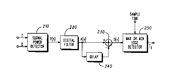
FIG. 2 illustrates a block diagram of an embodiment of a burst
detector according to the present invention. A signal power detector 210
detects a power magnitude P(n) of a combination of the digital in-phase
signal and the digital quadrature signal. A digital filter 220 having a
impulse response corresponding to a magnitude and duration of the
expected burst filters the power magnitude P(n) and produces a signal
to A(n). A subtractor 230 subtracts a delayed version of the signal A(n),
produced by a delay circuit 240, from the signal A(n) to provide the
detection signal D(n). An edge detector 250 detects an edge of the detection
signal D(n).
The digital filter 220 filters the power magnitude P(n) to reduce the
power of the noise. The result of this filtering increases the signal to noise
ratio and hence improves the quality of the detector. The digital filter 220
could be a finite impulse response (FIR) filter having characteristics close
to or approaching that of the expected burst. A digital filter 220 matched to
the expected burst would provide the maximum signal to noise ratio. The
2o digital filter 220, however, could be any filter that increases the signal
to
noise ratio.
The edge detector 250 detects an edge of the detection signal D(n)
and is clocked by the sample time of the timing circuit 130. The edge
detector 250 could use thresholds to detect the edge of the detection signal
D(n). Alternatively, the exemplary edge detector 250 in this embodiment
uses a maximum or minimum first, second, third or fourth approach to
determine a leading edge of the burst, as will be described below with
~1~043:~
.'
reference to FIG. 4. The edge detector 250 can also use a fifth approach
such as a pattern match approach.
FIG. 3 illustrates a timing diagram for the burst detector illustrating
signals A(n) and D(n) generated in response to art ideal square wave P(n).
The maximum and/or minimum of the detection signal D(n) of FIG. 3 can
be detected by the edge detector 250 in the below-discussed first, second or
third approaches to determine the leading edge of the burst. The time of
the signal A(n) can instead be detected in a fourth approach to determine
the leading edge of the signal as will be discussed below with respect to
io FIG. 4. Additionally, pattern matching of a shape of the detection signal
D(n) with an expected waveform such as, for example, the shape for signal
D(n) is illustrated in FIG. 3.
FIG. 4 illustrates implementations of an edge detector using
maximum and/or minimum threshold detectors 260, 280 and a timing
distance detector 270. The edge detector 250 detects one of or both the
maximum and minimum of the detection signal D(n) when using the
below-described first, second and third approaches. Although the
maximum threshold detector 260 and the minimum threshold detector
280 are preferably threshold detectors, any selector which identifies the
2o maximum and minimum is appropriate. In the first, second and third
approaches, the time of the maximum and/or the time of the minimum
can be determined by thresholding. The maximum threshold detector 260
thresholds the detection signal D(n) to determine if the maximum of the
detection D(n) is greater than a maximum threshold. The minimum
threshold detector 280 thresholds to determine if the detection signal D(n)
is less than a minimum threshold.
2~.~0~~1
_8_
A first approach in determining the leading edge of the burst is to
determine the time of the maximum and the time of the minimum of the
detection signal D(n). If the difference in the time of the maximum and
the time of the minimum is approximately equal to the duration of the
expected bursts, the leading edge of the burst can be determined from the
time of the maximum, the time of the minimum and the duration of the
expected bursts. The maximum is determined by the maximum threshold
detector 260 and the time of the minimum is determined by the
minimum threshold detector 280. The distance between the time of the
maximum and the time of the minimum is determined by the timing
distance detector 270. The timing distance detector 270 is provided by a
determining circuit connected to the maximum threshold detector 260 and
the minimum threshold detector 280 to determine a leading edge of the
burst based on an average of the time of the maximum and of the
minimum. The average of the time of the maximum and of the
minimum preferably is compared to one and one-half times the expected
length of the bursts. Therefore, the leading edge of the bursts is based on
an average of the time of the maximum and of the minimum less one
and one-half times the expected length of the burst.
2o A second approach would be to determine the time of the
maximum of the detection signal D(n). From the time of the maximum
detected by the maximum threshold detector 260 by itself and the duration
of the expected burst, the leading edge of the burst can be determined. The
illustrated minimum threshold detector 280 and the timing distance
detector 270 are not needed in this second approach.
A third approach would be to determine the time of the minimum
of the detection signal D(n). From the time of the minimum determined
21~0~3~.
-9-
by the minimum threshold detector 280 and the duration of the expected
burst, the leading edge of the burst can be determined. The illustrated
maximum threshold detector 260 -and the timing distance detector 270 are
not needed in this third approach.
Alternatively in a fourth approach, the leading edge of the burst
could be determined from detecting the time of the maximum of the
signal A(n). From the time of the maximum and the duration of the burst
the leading edge of the burst can be determined. In this fourth approach,
the time of the maximum can be determined by thresholding to
determine if the maximum of the detection signal D(n) is greater than a
maximum threshold. The maximum threshold detector 260 is thus
connected to receive signal A(n).
FIG. 5 illustrates a burst detector according to an alternative
embodiment of the present invention having a different configuration
capable of achieving the same result of the embodiment of FIG. 2. The
embodiment of FIG. 4 is mathematically equivalent to the embodiment of
FIG. 2. In the embodiment of FIG. 4 a signal power detector 310 detects a
power magnitude P(n) of a combination of the digital in-phase signal and
the digital quadrature signal. A digital filter 320 having a impulse
response corresponding to a magnitude and duration of the expected burst
filters the power magnitude P(n) and produces a signal A(n). A delay
circuit 340 delays the power magnitude P(n) and a moving average filter
360 filters the delayed power magnitude P(n). The moving average filter
360 also has a impulse response corresponding to a magnitude and
duration of the expected burst. A subtractor 330 subtracts an output of the
moving average filter 360 from the signal A(n) to provide the detection
~16~4~1
o-
signal D(n). An edge detector 350 detects an edge of the detection signal
D(n).
The edge detector 350 of FIG. 5 is illustrated by the exemplary
pattern match edge detector using a fifth approach. The pattern match
edge detector in block 350 of FIG. 5 contains a pattern match circuit to
pattern match a shape of the detection signal D(n) with an expected
waveform such as the shape of, for example, the waveform illustrated for
signal D(n) in the timing diagram of FIG. 3. However, the edge detector
350 can also be a maximum and/or minimum edge detector as discussed
1o above with respect to the first, second, third and fourth approaches.
Further, any arrangement for the filters and delays could use these and
other edge detector approaches.
FIG. 6 illustrates a detailed block diagram showing an alternative
implementation of the filters and the delays according to the present
invention. The moving average filters and delays of FIGS. 2 and 5, for
example, can be implemented by the illustrated configurations for the
delays 410, 420, 430 and 440 and by the illustrated connections
therebetween of the adders and subtractors 450, 460, 470, 480 and 490.
FIG. 7 illustrates a detailed block diagram showing another
2o alternative implementation of the filters and the delays of FIGS. 2 and 5,
for example, according to the present invention. Adders and subtractors
545, 550 and 560 are connected between delays 510, 520 and 530 as
illustrated. A multiplier 570 multiplies the output of the delay 510 by a
factor of two before providing an output to element 540.
Although the invention has been described and illustrated in the
above description and drawings, it is understood that this description is by
example only, and that numerous changes and modifications can be made
21~04~~
by those skilled in the art without departing from the true spirit and scope
of the invention. Thus the outputs of the timing circuit 130 may be
required by different circuits and not needed by all others. Although the
present invention exhibits Doppler shift tolerance, the present invention
provides additional advantages as mentioned herein and is thus
applicable to all radio communications systems regardless of the need for
Doppler shift tolerance such as paging, cellular and satellite
communication system receivers.
What is claimed is: