Note: Descriptions are shown in the official language in which they were submitted.
2160656
: 1 - CFO 10947 CA
-
ELECTRON SOURCE AND IMAGE FORMING APPARATUS
AS WELL AS METHOD OF PROVIDING THE SAME WITH MEANS
FOR MAINTAINING ACTIVATED STATE THEREOF
BACKGROUND OF THE INVENTION
Field of the Invention
This invention relates to an electron source and an
image forming apparatus and, more particularly, it
relates to an electron source provided with means for
maint~; n; ng it in an activated state by suppressing
degradation of and restoring the performance thereof
and an image forming apparatus comprising such an
electron source as well as a method of providing it
with such means.
Related Backqround Art
There have been known two types of electron-emitting
device; the thermionic cathode type and the cold
cathode type. Of these, the cold cathode refers to
devices including field emission type (hereinafter
referred to as the FE type) devices, metal/insulation
layer/metal type (hereinafter referred to as the MIM
type) electron-emitting devices and surface conduction
electron-emitting devices. Examples of FE type device
include those proposed by W. P. Dyke & W. W. Dolan,
"Field emission", Advance in Electron Physics, 8, 89
(19S6~ and C. A. Spindt, "PHYSICAL Properties of
thin-film field emission cathodes with molybdenium
2160656
_ - 2 -
cones", J. Appl. Phys., 47, 5284 (1976).
Examples of MIM device are disclosed in papers
including C. A. Mead, "The tunnel-emission amplifier",
J. Appl. Phys., 32, 646 (1961).
Examples of surface conduction electron-emitting
device include one proposed by M. I. Elinson, Radio
Eng. Electron Phys., 10, 1290 (1965).
A surface conduction electron-emitting device is
realized by utilizing the phenomenon that electrons are
emitted out of a small thin film formed on a substrate
when an electric current is forced to flow in parallel
with the film surface. While Elinson proposes the use
of SnO2 thin film for a device of this type, the use of
Au thin film is proposed in [G. Dittmer: "Thin Solid
Films", 9, 317 (1972)] whereas the use of In203/SnO2 and
that of carbon thin film are discussed respectively in
[M. Hartwell and C. G. Fonstad: "IEEE Trans. ED Conf.",
519 (1975~] and tH. Araki et al.: "Vacuum", Vol. 26,
No. 1, p.22 (1983)].
Fig. 27 of the accompanying drawings schematically
illustrates a typical surface conduction
electron-emitting device proposed by M. Hartwell. In
Fig. 27, reference numeral 1 denotes a substrate.
Reference numeral 4 denotes an electroconductive thin
film normally prepared by producing an H-shaped thin
metal oxide film by means of sputtering, part of which
eventually makes an electron-emitting region 5 when it
2160655
-- 3
is subjected to an electrically energizing process
referred to as "energization forming" as described
hereinafter. In Fig. 27, the thin horizontal area of
the metal oxide film separating a pair of device
electrodes has a length L of 0.5 to lmm and a width W'
of O.lmm.
Conventionally, an electron-emitting region 5 is
produced in a surface conduction electron-emitting
device by subjecting the electroconductive thin film 4
of the device to an electrically energizing prel; ; n~ry
process, which is referred to as "energization
forming". In the energization forming process, a
constant DC voltage or a slowly rising DC voltage that
rises typically at a rate of l V/min. is applied to
given opposite ends of the electroconductive thin film
4 to partly destroy, deform or transform the film and
produce an electron-emitting region 5 which is
electrically highly resistive. Thus, the
electron-emitting region 5 is part of the
electroconductive thin film 4 that typically contains a
fissure and fissures therein so that electrons may be
emitted from the fissure.
Currently available electron-emitting devices of the
type under consideration have room for improvement in
terms of performance and efficiency of electron
emission in order to realize image forming apparatuses
21606S5
-- 4
that provide bright and clear images on a stable basis.
The efficiency here refers to the ratio of the electric
current flowing through the surface conduction
electron-emitting device (hereinafter referred to as
"device current" or If) to the electric current formed
by electrons discharged from the device into vacuum
(hereinafter referred to as "emission current" or Ie)
when a voltage is applied to the paired device
electrodes of the device. An ideal electron-emitting
device will show a large emission current relative to a
small device current. If an electron-emitting device
is rigorously controllable for its electron emitting
performance and has an improved efficiency, an image
forming apparatus realized by arranging a number of
such electron-emitting devices and a fluorescent member
for forming images thereon will be able to produce high
quality images with a reduced energy consumption rate
if the apparatus is made very flat. Then, the drive
circuit of such an image forming apparatus can be
manufactured at reduced cost because of the low energy
consumption rate of the electron-emitting devices of
the apparatus.
However, the Hartwell's electron-emitting device does
not necessarily perform satisfactorily in terms of
stable emission of electrons and efficiency and,
therefore, it is thought to be very difficult to
realize an image forming apparatus that operates stably
2160656
to produce highly bright images with Hartwell's
devices.
As a result of intensive research efforts, the
inventors of the present invention discovered that, if
a certain voltage is applied to a surface conduction
electron-emitting device in an atmosphere that contains
organic subst~nces after producing an electron-emitting
region therein by energization forming as described
above, both If and Ie of the device remarkably
increase. This operation of applying a certain voltage
is termed "activation".
The above phenomenon of increased If and Ie is
attributable to an activated filmy deposit of carbon or
a carbon compound produced in the vicinity of the
electron-emitting region as a result of the voltage
application.
As an electron-emitting device is operated for a long
time for electron emission, the deposit in the vicinity
of the electron-emitting region may be gradually
decomposed and eroded to degrade the electron-emitting
performance of the device, although such degradation
may be suppressed by selecting appropriate parameters
for the activation process. This may be because the
crystallinity of the deposit affects the rate of
erosion and the crystallinity is by turn affected by
the parameters of the activation process. The use of a
metal having a high melting point such as tungsten for
216065~
~ - 6
;
the deposit is effective for suppressing the erosion of
the deposit.
Nevertheless, the performance of a surface conduction
electron-emitting device has to be further improved in
order to prevent degradation and prolong its service
life if it is to be used in an image forming apparatus
or a similar application.
In view of the above identified problems and other
problems, it is therefore an object of the present
invention to provide an improved surface conduction
electron-emitting device.
Additionally, the "activation process" requires the
use of a large vacuum apparatus provided with equipment
for introducing carbon and/or metal compounds into the
apparatus. When a large image forming apparatus having
a vacuum container (envelope) is subjected to an
activation process with such a vacuum apparatus, the
latter has to be provided with an exhaust pipe for
evacuating the inside of the vacuum container and
introducing carbon and/or metal compounds into the
vacuum container to make the overall operation rather
complicated and time consuming to push up the
manufacturing cost of the image forming apparatus
particularly if such compounds have a large molecular
weight. Thus, the present invention is also intended
to provide a method that allows the use of a down-sized
vacuum apparatus and a simplified manufacturing process
2160656
- 7
to bypass the above problems.
SUMMARY OF THE INVENTION
Therefore, it is an object of the present invention
to provide a method of suppressing degradation of and
restoring the electron emitting performance of an
electron source and an image forming apparatus
comprising such an electron source.
According to the invention, there is provided an
electron source comprising electron-emitting devices,
characterized in that it is provided with means for
supplying an activating substance to the
electron-emitting devices.
According to the invention, there is also provided an
image forming apparatus comprising an electron source
by turn comprising electron-emitting devices and an
image forming member to be irradiated with electron
beams from said electron source to form images thereon,
characterized in that said image forming apparatus is
provided with means for supplying an activating
substance to the electron-emitting devices.
According to the invention, there is also provided a
method of activating an electron source comprising
electron-emitting devices and an activating substance
source, characterized in that it comprises a step of
gasifying the activating substance from the activating
substance source and applying it to the
r-` 8 2 1 6 0 ~ 5
electron-emitting devices.
According to the invention, there is also provided a
method of activating an image forming apparatus
comprising an electron source by turn comprising
electron-emitting devices and an image forming member
to be irradiated with electron beams from said electron
source to form images thereon, characterized in that it
comprises a step of gasifying the activating substance
from the activating substance source and applying it to
the electron-emitting devices.
BRIEF DESCRIPTION OF THE DRAWINGS
Figs. lA through lC are schematic views of a surface
conduction electron-emitting device that can be used
for the purpose of the present invention.
Fig. 2 is a schematic view of another surface
conduction electron-emitting device that can be used
for the purpose of the present invention.
Fig. 3 is a schematic view of still another surface
conduction electron-emitting device that can be used
for the purpose of the present invention.
Figs. 4A through 4E are schematic views of a still
another electron-emitting device that can be used for
the purpose of the present invention, showing different
manufacturing steps.
Figs. 5A through 5D are graphs schematically showing
voltage waveforms that can be used for manufacturing
9 2160656
and gauging the performance of a surface conduction
electron-emitting device, an electron source comprising
such devices and an image forming apparatus comprising
such an electron source.
Fig. 6 is a block diagram of a measuring system for
determining the electron emitting performance of a
surface conduction electron-emitting device.
Fig. 7 is a graph showing a typical relationship
between the device voltage Vf and the device current If
and between the device voltage Vf and the emission
current Ie of a surface conduction electron-emitting
device or an electron source.
Fig. 8 is a schematic view of an embodiment of
electron source according to the invention.
Fig. 9A is a schematic view of an embodiment of image
forming apparatus according to the invention.
Fig. 9B is a schematic view of a getter arranged
within an image forming apparatus according to the
invention.
Fig. lOA and lOB are schematic views, illustrating
two possible configurations of fluorescent film of
display panel of an image forming apparatus according
to the invention.
Fig. 11 is a block diagram of a drive circuit of an
image forming apparatus for displaying images according
to NTSC system television signals.
Fig. 12 is a schematic view of another embodiment of
lO- 216065~
electron source according to the invention.
Fig. 13 is a schematic view of another embodiment of
image forming apparatus according to the invention.
Figs. 14A through 14D are schematic views of the
surface conduction electron-emitting device of Example
1.
Figs. 15A through 15J and Fig. 15L are schematic
views of the surface conduction electron-emitting
device of Example 1 in different manufacturing steps.
Figs. 16H, 16J and 16K are schematic views of the
surface conduction electron-emitting device of Example
3 in different manufacturing steps.
Figs. 17A through 17C are schematic views of the
surface conduction electron-emitting device of Example
4.
Figs. 18A through 18F are schematic views of the
electron source of Example 5 in different manufacturing
steps.
Fig. 19 is a schematic block diagram of a processing
apparatus that can be sued for manufacturing the image
forming apparatus of Example 5.
Fig. 20 is a schematic partial view of the electron
source of Example 7.
Fig. 21 is a schematic partial view of the electron
source of Example 7.
Figs. 22A through 22G are schematic views of the
electron source of Example 7 in different manufacturing
- - 11 21606~6
steps.
Figs. 23A and 23B are schematic views of the electron
source and the image forming apparatus of Example 7.
Fig. 24 is a schematic view of an electron source
according to the invention and having a matrix
arrangement, illustrating how it is wired for the steps
of energization forming and activation and an operation
of gauging its performance.
Fig. 25 is a schematic view of the image forming
apparatus of Example 7.
Fig. 26 is a block diagram illustrating an
application using the image-forming apparatus of
Example 9.
Fig. 27 is a schematic view of a known surface
conduction electron-emitting device.
DETAILED DESCRIPTION OF THE PREFERRED EMBODIMENTS
The present invention provides a method of
suppressing degradation of and restoring the electron
emitting performance of an electron source and an image
forming apparatus comprising such an electron source.
Such a method can be used in the "activation step" in
the process of manufacturing an electron source and an
image forming apparatus comprising such an electron
source to simplify the step. Additionally, such a
method can be used for suppressing degradation with
time of and temporarily restoring the electron emitting
`~ - 12 - 2160655
performance of an electron source and the
electron-emitting devices of an image forming
apparatus.
Now, the present invention will be described by
referring to the accompanying drawings that illustrate
preferred embodiments of the invention.
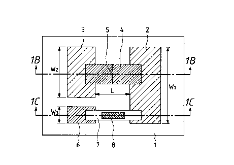
Figs. lA through lC are schematic views of a surface
conduction electron-emitting device of an electron
source according to the invention, of which Fig. lA is
a plan view and Figs. lB and lC are cross sectional
views taken along lines lB-lB and lC-lC respectively.
Referring to Figs. lA through lC, there are shown a
substrate 1, a pair of device electrodes 2 and 3, an
electroconductive thin film 4, an electron-emitting
region on 5, a film resistance heater 7 and an active
substance source 8, of which the film resistance heater
7 is arranged between one of the device electrodes, or
the electrode 2, and an electrode for supplying an
activating substance 6. Note that the device
electrodes 2 and 3 and the electroconductive thin film
4 including the electron-emitting region 5 constitute a
surface conduction electron-emitting device, while the
film resistance heater 7, the activating substance
source 8 and the electrodes 2 and 6 constitute an
activating substance supply means.
Materials that can be used for the substrate 1
include quartz glass, glass containing impurities such
- _ - 13 - 21 606~ 6
as Na to a reduced concentration level, soda lime
glass, glass substrate realized by forming an SiO2 layer
on soda lime glass by means of sputtering, ceramic
substances such as alumina as well as Si.
While the oppositely arranged device electrodes 2 and
3 and the electrode for supplying an activating
substance 6 may be made of any highly conducting
material, preferred candidate materials include metals
such as Ni, Cr, Au, Mo, W, Pt, Ti, Al, Cu and Pd and
their alloys, printable conducting materials made of a
metal or a metal oxide selected from Pd, Ag, Ru02, Pd-Ag
and glass, transparent conducting materials such as
In203-SnO2 and semiconductor materials such as
polysilicon.
The distance L separating the device electrodes, the
lengths W1 through W3 of the device electrodes and the
electrode for supplying an activating substance, the
contour of the electroconductive film 4 and other
factors for designing a surface conduction
electron-emitting device according to the invention may
be determined depending on the application of the
device. The distance L separating the device
electrodes 2 and 3 is preferably between several
hundred nanometers and several hundred micrometers and,
still preferably, between several micrometers and tens
of several micrometers.
The lengths W1 and W2 of the device electrodes 2 and
- 14 - 2160C56
3 is preferably between several micrometers and
hundreds of several micrometers depen~;ng on the
resistance of the electrodes and the electron-emitting
characteristics of the device. The film thickness d of
the device electrodes 2 and 3 is between tens of
several nanometers and several micrometers.
A surface conduction electron-emitting device that
can be used for the purpose of the present invention
may have a configuration other than the one illustrated
in Figs. lA through lC and, alternatively, it may be
prepared by laying a thin film 4 including an
electron-emitting region on a substrate 1 and then a
pair of oppositely disposed device electrodes 2 and 3
on the thin film.
The electroconductive thin film 4 is preferably a
fine particle film in order to provide excellent
electron-emitting characteristics. The thickness of
the electroconductive thin film 4 is determined as a
function of the step coverage of the electroconductive
thin film on the device electrodes 2 and 3, the
electric resistance between the device electrodes 2 and
3 and the parameters for the forming operation that
will be described later as well as other factors and
preferably between a tenth of a nanometer and hundreds
of several ~nl~ eters and more preferably between a
nanometer and fifty nanometers. The electroconductive
thin film 4 normally shows a resistance Rs between
_ - 15 - 2 16 06~ G
102 and 10' Q/O. Note that Rs is the resistance defined
by R=Rs(l/w), where t, w and l are the thickness, the
width and the length of the thin film respectively. R
is a resistance value measured along the direction of
the length l.
The electroconductive thin film 4 is made of fine
particles of a material selected from metals such as
Pd, Pt, Ru, Ag, Au, Ti, In, Cu, Cr, Fe, Zn, Sn, Ta, W
and Pb, oxides such as PdO, SnO2, In203, PbO and Sb2O3,
borides such as HfB2, ZrB2, LaB6, CeB6, YB4 and GdB4,
carbides such TiC, ZrC, HfC, TaC, SiC and WC, nitrides
such as TiN, ZrN and HfN, semiconductors such as Si and
Ge and carbon.
The term a "fine particle film" as used herein refers
to a thin film constituted of a large number of fine
particles that may be loosely dispersed, tightly
arranged or mutually and randomly overlapping (to form
an island structure under certain conditions). The
diameter of fine particles to be used for the purpose
of the present invention is between a tenth of a
n~n~ ?ter and hundreds of several nanometers and
preferably between a nanometer and twenty nanometers.
Since the term "fine particle" is frequently used
herein, it will be described in greater depth below.
A small particle is referred to as a "fine particle"
and a particle smaller than a fine particle is referred
to as an "ultrafine particle". A particle smaller than
216065S
- 16 -
an "ultrafine particle" and constituted by several
hundred atoms is referred to as a "cluster".
However, these definitions are not rigorous and the
scope of each term can vary depending on the particular
aspect of the particle to be dealt with. An "ultrafine
particle" may be referred to simply as a "fine
particle" as in the case of this patent application.
"The Experimental Physics Course No. 14: Surface/Fine
Particle" (ed., Koreo Kinoshita; Kyoritu Publication,
September 1, 1986) describes as follows.
"A fine particle as used herein referred to a
particle having a diameter somewhere between 2 to 3~m
and lOnm and an ultrafine particle as used herein means
a particles having a diameter somewhere between lOnm
and 2 to 3nm. However, these definitions are by no
means rigorous and an ultrafine particle may also be
referred to simply as a fine particle. Therefore,
these definitions are a rule of thumb in any means. A
particle constituted of two to several hundred atoms is
called a cluster." (Ibid., p.195, 11.22-26)
Additionally, "Hayashi's Ultrafine Particle Project"
of the New Technology Development Corporation defines
an "ultrafine particle" as follows, employing a smaller
lower limit for the particle size.
"The Ultrafine Particle Project (1981-1986) under the
Creative Science and Technology Promoting Scheme
defines an ultrafine particle as a particle having a
- 17 - 21 6065 6
;
diameter between about 1 and lOOnm. This means an
ultrafine particle is an agglomerate of about 100 to 108
atoms. From the viewpoint of atom, an ultrafine
particle is a huge or ultrahuge particle." (Ultrafine
Particle - Creative Science and Technology: ed.,
Chikara Hayashi, Ryoji Ueda, Akira Tazaki; Mita
Publication, 1988, p.2, 11.1-4) A particle smaller
than an ultrafine particle formed by several to several
hundred atoms is generally called a cluster." (Ibid:
p.2, 11.12-13)
Taking the above general definitions into
consideration, the term a "fine particle" as used
herein refers to an agglomerate of a large number of
atoms and/or molecules having a diameter with a lower
limit between several times of O.lnm and lnm and an
upper limit of several micrometers.
The electron-emitting region 5 is part of the
electroconductive thin film 4 and comprises an
electrically highly resistive fissure, although its
performance is dependent on the thickness and the
material of the electroconductive thin film 4 and the
energization forming process which will be described
hereinafter. The electron emitting region 5 may
contain in the inside fine particles having a diameter
between several times of a tenth of a nanometer and
tens of several nanometers. The material of such fine
particles may be selected from all or part of the
- 18 ~ 216065~
materials that can be used to prepare the thin film 4
including the electron emitting region. The electron
emitting region 5 and part of the thin film 4
surrounding the electron emitting region 5 may contain
carbon and carbon compounds.
If the activating substance is a carbide, the
activating substance source is preferably a thin film
of a baked or unbaked polymerized compound or a baked
or unbaked porous material that has adsorbed an organic
compound such as a hydrocarbon compound.
Polymerized compounds that can be used for the
purpose of the present invention include, polyvinyl
acetate, polyvinyl butyral, 3,5-dimethylphenol,
polyvinyl chloride. Any of these materials is used
after baking at temperature between 200 and 300C so
that it may produce little gas of the organic compound
if it is held in vacuum at room temperature. Examples
of carbon compounds that may be used for adsorption
include aromatic hydrocarbon compounds and olefinic
compounds.
If the activating substance is a metal compound and
the activation process is carried out by depositing a
high melting point metal such as W or Nb on the
electron-emitting region, materials that may be used
for the activating substance source include metal
halides such as fluorides, chlorides, bromides and
iodides, metal alkylates such as methylates, ethylates
`~ 19 2160656
and benzylates, metal ~-diketonates such as
acetylacetonates, dipivaloylmethanates and
hexafluoroacetylacetonates, metal enyl complexes such
as allyl complexes and cyclopentadienyl complexes,
arene complexes such as benzene complexes, metal
carbonyls and metal alkoxides as well as compounds
obtained by combining any of such substances. Specific
examples include NbF5, NbCl5, Nb(C5H5)(C0)4, Nb(C5H5)2Cl2,
OsF4, Os(C3H702) 3, OS ( CO ) 5, Os(C0) 12 ~ OS ( C5Hs ) 2 ~ ReF5 ~
ReCl5, Re(CO)1O, ReCl(CO)5, Re(CH3)(CO)5, Re(C5H5)(CO)3,
Ta(C5Hs)(C)4, Ta(OC2H5) 5 ~ Ta(C5H5)2Cl2, Ta(C5H5)2H3 WF6,
W(C0)6, W(C5H5)2C12, W(C5H5)2H2 and W(CH3)6. Of these,
W( C ) 6 ( tungsten hexacarbonyl) is preferable because it
can be used to produce tungsten which is a metal having
a high melting point and handled relatively easily.
In the above described electron-emitting device, the
activating substance source 8 is formed on the film
resistance heater 7, which is designed to be heated and
to evaporate the activating substance of the activating
substance source 8 as a voltage is applied to the
device electrode 2 and the electrode for supplying an
activating substance 6 to cause an electric current to
flow through the heater 7. The evaporated substance is
eventually fed to and near the electron-emitting
region. The film resistance heater 7 may be made of a
metal such as Au, Pt or Ni or an electroconductive
oxide such as SnO2-In203(IT0). In stead of a thin film,
~ 20 216065B
the heater may be realized in the form of a wire.
In the above described electron-emitting device, one
of the device electrodes also operates as an electrode
for feeding the film resistance heater with electricity
(electrode for supplying an activating substance).
Alternatively, however, a pair of electrodes for
supplying an activating substance may be arranged
independently of the device electrodes. Still
alternatively, activating substance source and film
resistance heater may be arranged on both lateral side
of the electron-emitting region. The positional
arrangement of these components may be appropriately
modified so long as the activating substance can be
effectively fed to and near the electron-emitting
region.
For the purpose of the invention, step type surface
conduction electron-emitting devices each having a
profile as illustrated in Fig. 2 may be used in place
of devices each having a profile of lB, which is a
sectional view taken along line lB-lB in Fig. lA. In
Fig. 2, reference numeral 10 denotes a step forming
member typically made of an electrically insulating
material.
The method of supplying an activating substance from
the activating substance source according to the
invention may be so modified that, in place of passing
electric current through and heating the film
- 21 - 216065B
resistance heater, electron beams emitted from the
electron-emitting device may be used to irradiate the
activating substance source in order to supply the
activating substance to and near the electron-emitting
region. Fig. 3 schematically illustrates the
arrangement of the electron source for such a modified
method. Then, the electrode for supplying an
activating substance 6 is subjected to a voltage higher
than that of the anode of the corresponding surface
conduction electron-emitting device comprising a pair
of device electrodes 2 and 3 and an electroconductive
thin film 5 including an electron-emitting region 5 so
that it may attract electrons emitted from the
electron-emitting region 5 and cause them to collide
with the activating substance source 8, which is
consequently energized and supplies the activating
substance to and near the electron-emitting region.
Now, a method of manufacturing a surface conduction
electron-emitting device having a configuration as
described above will be described by referring to Figs.
lA through lC and 4A through 4E.
1) After thoroughly cleansing a substrate 1 with
detergent and pure water, a material is deposited on
the substrate 1 (as shown in Fig. 4A which is a cross
sectional view taken along line lB-lB in Fig. lA) by
means of vacuum evaporation, sputtering or some other
appropriate technique for a pair of device electrodes 2
_ - 22 - ~ 21 6065 S
and 3 and an electrode for supplying an activating
substance 6, which are then patterned with
photolithography technique or the like (Fig. 4B).
2) An organic metal thin film is formed on the
substrate 1 carrying thereon the pair of device
electrodes 2 and 3 and an electrode for supplying an
activating substance 6 by applying an organic metal
solution and leaving the applied solution for a given
period of time. The organic metal solution may contain
as a principal ingredient any of the metals listed
above for the electroconductive thin film 4.
Thereafter, the organic metal thin film is heated,
baked and subsequently subjected to a patterning
operation, using an appropriate t~chn;que such as
lift-off or etching, to produce an electroconductive
thin film 4 (Fig. 4C which is a cross sectional view
also taken along line lB-lB in Fig. lA). While an
organic metal solution is applied to produce a thin
film in the above description, an electroconductive
thin film 4 may alternatively be formed by vacuum
evaporation, sputtering, chemical vapor deposition,
dispersed application, dipping, spinner or some other
technique.
3~ Then, a film resistance heater 7 and an activating
substance source 8 are formed. Any method that may be
used for forming an electroconductive thin film 4 may
also be used for the film resistance heater 7.
~ - 23 _ ~21606S~
Subsequently, the activating substance source 8 is
formed thereon and, if necessary, subjected to other
processing operations such as baking (Fig. 4D which is
a cross sectional view also taken along line lC-lC in
Fig. lA).
4) Thereafter, the device electrodes 2 and 3 are
subjected to a process referred to as "forming". Here,
an energization forming process will be described as a
choice for forming. More specifically, voltage is
applied between the device electrodes 2 and 3 by means
of a power source (not shown) until an electron
emitting region (fissures) 5 is produced in a given
area of the electroconductive thin film 4 to show a
modified structure that is different from that of the
electroconductive thin film 4 ~Fig. 4E which is a cross
sectional view also taken along line lB-lB in Fig. lA).
Figs. 5A through 5D show different pulse voltages that
can be used for energization forming.
The voltage to be used for energization forming
preferably has a pulse waveform. A pulse voltage
having a constant height or a constant peak voltage may
be applied continuously as shown in Fig. 5A or,
alternatively, a pulse voltage having an increasing
height or an increasing peak voltage may be applied as
2 5 shown in Fig. 5B.
In Fig. 5A, the pulse voltage has a pulse width T
and a pulse interval T2, which are typically between
21606S6
- 24 -
l~sec. and lOmsec. and between lO~sec. and lOOmsec.
respectively. The height of the triangular wave (the
peak voltage for the energization forming operation)
may be appropriately selected depending on the profile
of the surface conduction electron-emitting device.
The voltage is typically applied for a period between
several seconds and tens of several minutes in vacuum.
Note, however, that the pulse waveform is not limited
to triangular and a rectangular or some other waveform
may alternatively be used.
Fig. 5B shows a pulse voltage whose pulse height
increases with time. In Fig. 5B, the pulse voltage has
an width T1 and a pulse interval T2 that are
substantially similar to those of Fig. 5A. The height
of the triangular wave (the peak voltage for the
energization forming operation) is, however, increased
at a rate of, for instance, O.lV per step.
The energization forming operation will be terminated
by measuring the current running through the device
electrodes when a pulse voltage that is sufficiently
low and does not locally destroy or deform the
electroconductive thin film 2, or about O.lV, is
applied to the device between the pulses for the
energization forming. Typically the energization
forming operation is terminated when a resistance
greater than lMQ is observed for the device current
rllnni n9 through the electroconductive thin film 4 while
_ - 25 ~ 21606~6
applying a pulse voltage of approximately O.lV to the
device electrodes.
5) After the energization forming operation, the
electron-emitting device is subjected to an activation
process.
In an activation process, a pulse voltage is
repeatedly applied to the device in a vacuum chamber,
in which a carbon compound or a metal compound
(activating substance) exists at a very small
concentration. As a result of this process, carbon, a
carbon compound or a metal compound is deposited on the
electron-emitting region so that device current If and
the emission current Ie change remarkably. The
activation step is conducted, observing the device
current If and the emission current Ie, and terminated
when the emission current Ie gets to a saturated level,
for instance.
The activating substance may be supplied by passing
electric current through the film resistance heater 7
formed in the preceding step and evaporating the
activating substance in the activating substance source
8 or by introducing an appropriate substance from a
substance feeding device fitted to the vacuum
apparatus.
If a carbon compound is used as an activating
substance, a component of oil diffusing within the
vacuum chamber from an exhaust system equipped with a
216065S
- 26 -
-
diffusion pump or a rotary pump involving the use of
oil may be utilized. Alternatively, a carbon compound
may be introduced into the vacuum chamber after
evacuating the inside of the apparatus by means of a
ultrahigh vacuum system equipped with an ion pump.
Subst~nc~ that can be suitably used for the purpose of
the activation process include aliphatic hydrocarbons
such as alkanes, alkenes and alkynes, aromatic
hydrocarbons, alcohols, aldehydes, ketones, amines,
organic acids such as phenol, carbonic acids and
sulfonic acids. Specific examples include saturated
hydrocarbons expressed by general formula CnH2n~2 such as
methane, ethane and propane, unsaturated hydrocarbons
expressed by general formula CnH2n such as ethylene and
propylene, benzene, toluene, methanol, ethanol,
formaldehyde, acetaldehyde, acetone, methylethylketone,
methylamine, ethylamine, phenol, formic acid, acetic
acid and propionic acid.
If a metal compound is used as an activating
substance, any of the metal compounds listed above by
referring to the activating substance source may be
used.
The pulse waveform of the voltage applied to the
electron-emitting device in this activation step may be
rectangular as shown in Fig. 5C. Alternatively, an
alternating rectangular pulse waveform that alternately
changes the polarity as shown in Fig. 5D may be used.
`- - 27 _ ~ 21 6 06~ 5
6) An electron-emitting device that has been treated
in an energization forming process and an activation
process is then preferably subjected to a stabilization
process. This is a process for removing any activating
substance remaining in the vacuum chamber typically
through adsorption except the substance existing in the
activating substance source 8 arranged on the electron
source. The vacuuming and exhausting equipment to be
used for this process preferably does not involve the
use of oil so that it may not produce any evaporated
oil that can adversely affect the performance of the
treated device during the process. Thus, the use of a
sorption pump and an ion pump may be a preferable
choice.
The partial pressure of the activating substance in
the vacuum chamber is preferably lower than lxlO~6Pa and
more preferably lower than lxlO~BPa, in which no carbon
or carbon compound is additionally deposited. The
vacuum chamber is preferably heated during evacuating
so that organic molecules adsorbed by the inner walls
of the vacuum chamber and the electron-emitting
device(s) in the chamber may also be easily eliminated.
While the vacuum chamber is preferably heated to 80 to
250C for more than 5 hours in most cases, other
heating conditions may alternatively be selected
depending on the size and the profile of the vacuum
_ - 28 ~ 2160656
chamber and the configuration of the electron-emitting
device(s) in the chamber as well as other consider-
ations. The pressure in the vacuum chamber needs to be
made as low as possible and it is preferably lower than
lxlO~sPa and more preferably lower than lxlO~6Pa.
After the stabilization process, the atmosphere for
driving the electron-emitting device or the electron
source is preferably same as the one when the
stabilization process is completed, although a lower
pressure may alternatively be used without damaging the
stability of operation of the electron-emitting device
or the electron source if the activating substance in
the chamber is sufficiently removed.
By using such a vacuum like atmosphere, the formation
of any additional deposit of carbon or a carbon
compound can be effectively suppressed and the H20, 2
and other substances adsorbed to the inner wall surface
of the envelope (vacuum chamber) and the outer surface
of the substrate can be removed to consequently
stabilize the device current If and the emission
current Ie.
As described earlier, the carbon, carbon compound or
metal deposited on the electron-emitting region can
erode to degrade the electron emitting performance of
the device but such degradation in the performance of
the device can be prevented by passing electric current
through the film resistance heater and supplying the
- 29 - 21606S~
activating substance from the activating substance
source at a reduced rate in a controlled manner so that
the activating substance may not be supplied
excessively. Alternatively, the performance of the
device may be checked periodically and, if the detected
degradation is not negligible, the activating substance
may be supplied to the electron-emitting region to
recover the performance so that the device may get rid
of any practical degradation of performance.
While an electron-emitting device of Fig. 3 is
prepared substantially in a manner as described above,
the activation step is limited to the technique of
introducing an activating substance. With such an
electron-emitting device, degradation in the
performance of the device may be prevented and a
degraded performance of the device may be recovered by
feeding part of the electrons emitted from it toward
the activating substance source and cause them to
collide with the activating substance so that the
activating substance may be additionally supplied to
the electron-emitting region.
The performance of an electron-emitting device
prepared by way of the above processes, to which the
present invention is applicable, will be described by
referring to Figs. 6 and 7.
Fig. 6 is a schematic block diagram of an arrangement
of a vacuum treatment equipment that can be used for
~1606~
- 30 -
the above processes. It can also be used as a
measuring system for determining the performance of an
electron emitting device of the type under
consideration. Referring to Fig. 6, refference numeral
16 denotes a vacuum chamber and reffernce numeral 17
denotes a vacuum pump. An electron-emitting device is
placed in the vacuum chamber 16. The device comprises
a substrate 1, a pair of device electrodes 2 and 3, a
thin film 4 and an electron-emitting region 5.
Otherwise, the measuring system has a power source 11
for applying a device voltage Vf to the device, an
ammeter 12 for metering the device current If running
through the thin film 4 between the device electrodes 2
and 3, an anode 15 for capturing the emission current
Ie produced by electrons emitted from the
electron-emitting region of the device, a high voltage
source 14 for applying a voltage to the anode 15 of the
measuring system and another ammeter 13 for metering
the emission current Ie produced by electrons emitted
from the electron-emitting region 5 of the device. For
determining the performance of the electron-emitting
device, a voltage between 1 and 10kV may be applied to
the anode, which is spaced apart from the electron
emitting device by distance H which is between 2 and
8mm.
Instruments including a pressure gauge and other
pieces of equipment necessary for measuring an
- 31 - ~21606~
atmosphere in the vacuum chamber 16 so that the
performance of the electron-emitting device or the
electron source may be properly tested under desired
atmosphere. The vacuum pump 17 may be provided with an
ordinary high vacuum system comprising a turbo pump and
a rotary pump or the like, and an ultra-high vacuum
system comprising an ion pump or the like. The entire
vacuum chamber containing an electron source substrate
therein can be heated by means of a heater (not shown).
While not shown in Figs. 6 and 7, the measuring system
is also provided with a power source for applying a
voltage to the electrode for supplying an activating
substance so that, whenever necessary, a selected
voltage may be applied to the electrode for supplying
an activating substance in a coordinated manner as
another voltage is applied to the device electrodes
from the power source 11. In short the steps from the
energization forming step on can be carried out with
the above described vacuum arrangement.
Fig. 7 shows a graph schematically illustrating the
relationship between the device voltage Vf and the
emission current Ie and the device current If typically
observed by the measuring system of Fig. 6. Note that
different units are arbitrarily selected for Ie and If
in Fig. 7 in view of the fact that Ie has a magnitude
by far smaller than that of If. Note that both the
vertical and horizontal axes of the graph represent a
~ - 32 - 21606S~
linear scale.
As seen in Fig. 7, an electron-emitting device that
can be used for the purpose of the invention has three
remarkable features in terms of emission current Ie,
which will be described below.
(i) Firstly, an electron-emitting device according to
the invention shows a sudden and sharp increase in the
emission current Ie when the voltage applied thereto
exceeds a certain level (which is referred to as a
threshold voltage hereinafter and indicated by Vth in
Fig. 7), whereas the emission current Ie is practically
undetectable when the applied voltage is found lower
than the threshold value Vth. Differently stated, an
electron-emitting device according to the invention is
a non-linear device having a clear threshold voltage
Vth to the emission current Ie.
(ii) S~con~ly~ since the emission current Ie is
highly dependent on the device voltage Vf, the former
can be effectively controlled by way of the latter.
(iii) Thirdly, the emitted electric charge captured
by the anode 15 is a function of the duration of time
of application of the device voltage Vf. In other
words, the amount of electric charge captured by the
anode 15 can be effectively controlled by way of the
time during which the device voltage Vf is applied.
Because of the above remarkable features, it will be
understood that the electron-emitting behavior of a
216065~
~ - 33 -
surface conduction electron-emitting device that can be
used for the purpose of the invention can be controlled
as a function of the input signal. Thus, an electron
source may be realized by arranging a number of such
electron-emitting devices, taking advantage of this
controllability, and then such an electron source may
be used for an image forming apparatus or some other
possible application.
Referring to Fig. 7, the device current If
monotonically increases relative to the device voltage
Vf (referred to as "MI characteristic" hereinafter).
However, it may so change as to show a curve (not
shown) specific to a voltage-controlled-negative-
resistance characteristic (a characteristic referred to
as "VCNR characteristic" hereinafter). These
characteristics of the device current can be controlled
by conducting the above steps in a controlled manner.
The VCNR characteristic may become apparent when the
activating substance is supplied excessively to the
electron-emitting region by the means for supplying the
activating substance.
A linear or a planar electron source may be realized
by arranging a number of surface conduction
electron-emitting devices on an insulating substrate
and wiring them appropriately. Then, an image forming
apparatus may be produced by using such an electron
source.
2160656
- 34 -
Electron-emitting devices may be arranged on a
substrate in a number of different modes.
For instance, a number of electron-emitting devices
may be arranged in parallel rows along a direction
(hereinafter referred to row-direction), each device
being connected by wires at opposite ends thereof, and
driven to operate by control electrodes (hereinafter
referred to as grids) arranged in a space above the
electron-emitting devices along a direction
perpendicular to the row direction (hereinafter
referred to as column-direction) to realize a
ladder-like arrangement. Alternatively, a plurality of
electron-emitting devices may be arranged in rows along
an X-direction and columns along a Y-direction to form
a matrix, the X- and Y-directions being perpendicular
to each other, and the electron-emitting devices on the
same row are connected to a common X-directional wire
by way of one of the electrodes of each device while
the electron-emitting devices on a same column are
connected to a common Y-directional wire by way of the
other electrode of each device. The latter arrangement
is referred to as a simple matrix arrangement. Now,
the simple matrix arrangement will be described in
detail.
In view of the above described three basic
characteristic features (i) through (iii) of a surface
conduction electron-emitting device, to which the
_ ~ 35 ~ 2160656
invention is applicable, it can be controlled for
electron emission by controlling the wave height and
the wave width of the pulse voltage applied to the
opposite electrodes of the device above the threshold
voltage level. On the other hand, the device does not
practically emit any electron below the threshold
voltage level. Therefore, regardless of the number of
electron-emitting devices arranged in an apparatus,
desired surface conduction electron-emitting devices
can be selected and controlled for electron emission in
response to an input signal by applying a pulse voltage
to each of the selected devices.
Fig. 8 is a schematic plan view of the substrate of
an electron source realized by arranging a plurality of
electron-emitting devices, to which the present
invention is applicable, in order to exploit the above
characteristic features. In Fig. 8, the electron
source comprises a substrate 21, X-directional wires
22, Y-directional wires 23, wires for supplying an
activating substance 26, surface conduction
electron-emitting devices 24, connecting wires 25 and
means for supplying an activating substance 27
consisting of a film resistance heater and an
activating substance source. The surface conduction
electron-emitting devices 24 may be either of the flat
type or of the step type described earlier.
There are provided a total of m X-directional
216065~
- 36 -
wires 22, which are denoted by Dxl, Dx2, ..., Dxm
respectively and made of an electroconductive metal
produced by vacuum evaporation, printing or sputtering.
These wires are appropriately designed in terms of
material, thickness and width. A total of n
Y-directional wires 23 are arranged and denoted by Dyl,
Dy2, ..., Dyn respectively, which are similar to the
X-directional wires in terms of material, thickness and
width. There are also provides a total of m wires for
supplying an activating substance 26, which are denoted
by Axl, Ax2, ..., Axm respectively and arranged like
the X- and Y-directional wires. An interlayer
insulation layer (not shown) is disposed between the
m X-directional wires 22 and the m wires for supplying
an activating substance 26 and the n Y-directional
wires to electrically isolate them. (Both m and n are
integers.)
The interlayer insulation layer (not shown) is
typically made of SiO2 and formed on the entire surface
or part of the surface of the insulating substrate 21
carrying the X-directional wires 22 and the wires for
supplying an substrate 26 to show a desired contour by
means of vacuum evaporation, printing or sputtering.
The thickness, material and manufacturing method of the
interlayer insulation layer are so selected as to make
it withstand the potential difference between any of
the X-directional wires 22 and the wires for supplying
- - 37 - 2 1 6 0 6 5 6
an activating substance 26 and any of the Y-directional
wire 23 observable at the crossing thereof. Each of
the X-directional wires 22, the wires for supplying an
activating substance 26 and the Y-directional wires 23
is drawn out to form an external terminal.
The oppositely arranged electrodes (not shown) of
each of the surface conduction electron-emitting
devices 24 are connected to related one of the
m X-directional wires 22 and related one of the
n Y-directional wires 23 by respective connecting wires
25 which are made of an electroconductive metal.
The electroconductive metal material of the device
electrodes and that of the wires 22 and 23 and the
connecting wires 25 may be same or contain a common
element as an ingredient. Alternatively, they may be
different from each other. These materials may be
appropriately selected typically from the candidate
materials listed above for the device electrodes. If
the device electrodes and the connecting wires are made
of a same material, they may be collectively called
device electrodes without discriminating the connecting
wires.
The X-directional wires 22 are electrically connected
to a scan signal application means (not shown) for
applying a scan signal to a selected row of surface
conduction electron-emitting devices 24. On the other
hand, the Y-directional wires 23 are electrically
- 38 21 6 0656
connected to a modulation signal generation means (not
shown) for applying a modulation signal to a selected
column of surface conduction electron-emitting devices
24 and modulating the selected column according to an
input signal. Note that the drive signal to be applied
to each surface conduction electron-emitting device is
expressed as the voltage difference of the scan signal
and the modulation signal applied to the device.
With the above arrangement, each of the devices can
be selected and driven to operate independently by
means of a simple matrix wire arrangement.
On the other hand, the means for supplying an
activating substance can be driven to supply an
activating substance on a line by line basis as an
appropriate voltage is applied between a selected
X-directional wire 26 and a corresponding wire for
supplying an activating substance 26.
Now, an image-forming apparatus comprising an
electron source having a simple matrix arrangement as
described above will be described by referring to Figs.
9A, 10A, lOB and 11. Fig. 9A is a partially cut away
schematic perspective view of the image forming
apparatus and Figs. 10A and lOB are schematic views,
illustrating two possible configurations of a
fluorescent film that can be used for the image forming
apparatus of Fig. 9A, whereas Fig. 11 is a block
diagram of a drive circuit for the image forming
_ ~ 39 ~ 21 606,5 6
apparatus that operates with NTSC television signals.
Referring firstly to Fig. 9A illustrating the basic
configuration of the display panel of the image-forming
apparatus, it comprises an electron source substrate 21
of the above described type carrying thereon a
plurality of electron-emitting devices, a rear plate 31
rigidly holding the electron source substrate 21, a
face plate 36 prepared by laying a fluorescent film 34
and a metal back 35 on the inner surface of a glass
substrate 33 and a support frame 32, to which the rear
plate 31 and the face plate 36 are bonded by means of
frit glass. Reference numeral 37 denote an envelope,
which is baked to 400 to 500C for more than 10 minutes
in the atmosphere or in nitrogen and hermetically and
airtightly sealed.
In Fig. 9A, reference numeral 24 denotes each of the
electron-emitting devices and reference numerals 22 and
23 respectively denotes the X-directional wire and the
Y-directional wires connected to the respective device
electrodes of each of the electron-emitting devices.
While the envelope 37 is formed of the face plate 36,
the support frame 32 and the rear plate 31 in the above
described embodiment, the rear plate 31 may be omitted
if the substrate 21 is strong enough by itself because
the rear plate 31 is provided mainly for reinforcing
the substrate 21. If such is the case, an independent
rear plate 31 may not be required and the substrate 21
" -
~ 40 ~ ~1606~ 6
may be directly bonded to the support frame 32 so that
the envelope 37 is constituted of a face plate 36, a
support frame 32 and a substrate 21. The overall
strength of the envelope 37 may be increased by
arranging a number of support members called spacers
(not shown) between the face plate 36 and the rear
plate 31.
Figs. lOA and lOB schematically illustrate two
possible arrangements of fluorescent film. While the
fluorescent film 34 comprises only a single fluorescent
body if the display panel is used for showing black and
white pictures, it needs to comprise for displaying
color pictures black conductive members 38 and
fluorescent bodies 39, of which the former are referred
to as black stripes or members of a black matrix
depending on the arrangement of the fluorescent bodies.
Black stripes or members of a black matrix are arranged
for a color display panel so that the fluorescent
bodies 39 of three different primary colors are made
less discriminable and the adverse effect of reducing
the contrast of displayed images of external light is
weakened by blacke~;ng the surrounding areas. While
graphite is normally used as a principal ingredient of
the black stripes, other conductive material having low
light transmissivity and reflectivity may alternatively
be used.
A precipitation or printing technique is suitably be
. - 41 - 216065 6
used for applying a fluorescent material on the glass
substrate regardless of black and white or color
display. An ordinary metal back 35 is arranged on the
inner surface of the fluorescent film 34. The metal
back 35 is provided in order to enhance the lllm;n.~nce
of the display panel by causing the rays of light
emitted from the fluorescent bodies and directed to the
inside of the envelope to turn back toward the face
plate 36, to use it as an electrode for applying an
accelerating voltage to electron beams and to protect
the fluorescent bodies against damages that may be
caused when negative ions generated inside the envelope
collide with them. It is prepared by smoothing the
inner surface of the fluorescent film (in an operation
normally called "filming") and forming an Al film
thereon by vacuum evaporation after forming the
fluorescent film.
A transparent electrode (not shown) may be formed on
the face plate 36 facing the outer surface of the
fluorescent film 34 in order to raise the conductivity
of the fluorescent film 34.
Care should be taken to accurately align each set of
color fluorescent bodies and an electron-emitting
device, if a color display is involved, before the
above listed components of the envelope are bonded
together.
An image forming apparatus as illustrated in Fig. 9A
- 42 _ 216065~
is typically prepared in a manner as described below.
The envelope 37 is evacuated by means of an
appropriate vacuum pump such as an ion pump or a
sorption pump that does not involve the use of oil,
while it is being heated as in the case of the
abovedescribed stabilization process, until the
atmosphere in the inside is reduced to a degree of
vacuum of 10~5Pa containing an organic substance to a
sufficiently low level and then it is hermetically and
airtightly sealed. A getter process may be conducted
in order to maintain the achieved degree of vacuum in
the inside of the envelope 37 after it is sealed. In a
getter process, a getter arranged at a predetermined
position in the envelope 37 is heated by means of a
resistance heater or a high frequency heater to form a
film by vapor deposition ir~o.~; ately before or after
the envelope 37 is sealed. A getter typically contains
Ba as a principal ingredient and can maintain pressure
between 1.3x10⁻⁴ and 1.3x10⁻⁵ Pa by the adsorption effect
of the vapor deposition film. The steps from the
energization forming step on to be conducted on the
surface conduction electron-emitting devices may be
carried out appropriately as described earlier.
If a getter process is repeated for a number of times
as will be described hereinafter, an amount of getter
that exceeds the amount to be consumed in this step
should be arranged inside the envelope 37. For
- 43 - 216065 6
instance, a getter 28 may be arranged between the
envelope 37 and the electron source substrate 21 as
schematically illustrated in Fig. 9B. Protecting wall
29 may be arranged to prevent an evaporated getter
material from depositting on the electron source
substrate to form a getter film there.
Now, a drive circuits for driving a display panel
comprising an electron source with a simple matrix
arrangement for displaying television images according
to NTSC television signals will be described by referring
to Fig. 11. In Fig. 11, reference numeral 41 denotes a
display panel. Otherwise, the circuit comprises a scan
circuit 42, a control circuit 43, a shift register 44,
a line memory 45, a synchronizing signal separation
circuit 46 and a modulation signal generator 47. Vx
and Va in Fig. 11 denote DC voltage sources.
The display panel 41 is connected to external
circuits via terminals Doxl through Doxm, Doyl through
Doyn and high voltage terminal Hv, of which terminals
Doxl through Doxm are designed to receive scan signals
for sequentially driving on a one-by-one basis the rows
(of N devices) of an electron source in the apparatus
comprising a number of surface-conduction type
electron-emitting devices arranged in the form of a
matrix having M rows and N columns.
On the other hand, terminals Doyl through Doyn are
designed to receive a modulation signal for controlling
_ ~ 44 ~ 2160656
;
the output electron beam of each of the
surface-conduction type electron-emitting devices of a
row selected by a scan signal. High voltage terminal
Hv is fed by the DC voltage source Va with a DC voltage
of a level typically around lOkV, which is sufficiently
high to energize the fluorescent bodies of the selected
surface-conduction type electron-emitting devices.
The scan circuit 42 operates in a r~nn~ as follows.
The circuit comprises M switching devices (of which
only devices S1 and Sm are specifically indicated in
Fig. 13), each of which takes either the output voltage
of the DC voltage source Vx or O[V] (the ground
potential level) and comes to be connected with one of
the terminals Doxl through Doxm of the display panel
41. Each of the switching devices S1 through Sm
operates in accordance with control signal Tscan fed
from the control circuit 43 and can be prepared by
combining transistors such as FETs.
The DC voltage source Vx of this circuit is designed
to output a constant voltage such that any drive
voltage applied to devices that are not being scanned
due to the performance of the surface conduction
electron-emitting devices (or the threshold voltage for
electron emission) is reduced to less than threshold
voltage.
The control circuit 43 coordinates the operations of
related components so that images may be appropriately
~ _ ~ 45 ~ 21 60 6 5 6
displayed in accordance with externally fed video
signals. It generates control signals Tscan, Tsft and
Tmry in response to synchronizing signal Tsync fed from
the synchronizing signal separation circuit 46, which
will be described below.
The synchronizing signal separation circuit 46
separates the synchronizing signal component and the
luminance signal component form an externally fed NTSC
television signal and can be easily realized using a
popularly known frequency separation (filter) circuit.
Although a synchronizing signal extracted from a
television signal by the synchronizing signal
separation circuit 46 is constituted, as well known, of
a vertical synchronizing signal and a horizontal
synchronizing signal, it is simply designated as Tsync
signal here for convenience sake, disregarding its
component signals. On the other hand, a luminance
signal drawn from a television signal, which is fed to
the shift register 44, is designed as DATA signal.
The shift register 44 carries out for each line a
serial/parallel conversion on DATA signals that are
serially fed on a time series basis in accordance with
control signal Tsft fed from the control circuit 43.
(In other words, a control signal Tsft operates as a
shift clock for the shift register 44.) A set of data
for a line that have undergone a serial/parallel
conversion (and correspond to a set of drive data for N
_ - 46 ~ 216065 6
electron-emitting devices) are sent out of the shift
register 44 as N parallel signals Idl through Idn.
The line memory 45 is a memory for storing a set of
data for a line, which are signals Idl through Idn, for
a required period of time according to control signal
Tmry coming from the control circuit 43. The stored
data are sent out as signals I'dl through I'dn to a
modulation signal generator 47.
Said modulation signal generator 47 is in fact a
signal source that appropriately drives and modulates
the operation of each of the surface-conduction type
electron-emitting devices according to each of the
image data I'dl through I'dn and output signals of this
device are fed to the surface-conduction type
electron-emitting devices in the display panel 41 via
terminals Doyl through Doyn.
As described above, an electron-emitting device, to
which the present invention is applicable, is
characterized by the following features in terms of
emission current Ie. Firstly, there exists a clear
threshold voltage Vth and the device emit electrons
only a voltage exceeding Vth is applied thereto.
Secondly, the level of emission current Ie changes as a
function of the change in the applied voltage above the
threshold level Vth. More specifically, when a
pulse-shaped voltage is applied to an electron-emitting
device according to the invention, practically no
~ 47 ~ 216 065 6
emission current is generated so far as the applied
voltage r~i ns under the threshold level, whereas an
electron beam is emitted once the applied voltage rises
above the threshold level. It should be noted here
that the intensity of an output electron beam can be
controlled by changing the peak level Vm of the
pulse-shaped voltage. Additionally, the total amount
of electric charge of an electron beam can be
controlled by varying the pulse width Pw.
Thus, either a voltage modulation method or a pulse
width modulation method may be used for modulating an
electron-emitting device in response to an input
signal. With voltage modulation, a voltage modulation
type circuit is used for the modulation signal
generator 47 so that the peak level of the pulse shaped
voltage is modulated according to input data, while the
pulse width is held constant.
With pulse width modulation, on the other hand, a
pulse width modulation type circuit is used for the
modulation signal generator 47 so that the pulse width
of the applied voltage may be modulated according to
input data, while the peak level of the applied voltage
is held constant.
Although it is not particularly mentioned above, the
shift register 44 and the line memory 45 may be either
of digital or of analog signal type so long as
serial/parallel conversions and storage of video
- 2160656
- - 48 -
signals are conducted at a given rate.
If digital signal type devices are used, output
signal DATA of the synchronizing signal separation
circuit 46 needs to be digitized. However, such
conversion can be easily carried out by arranging an
A/D converter at the output of the synchronizing signal
separation circuit 46. It may be needless to say that
different circuits may be used for the modulation
signal generator 47 depending on if output signals of
the line memory 45 are digital signals or analog
signals. If digital signals are used, a D/A converter
circuit of a known type may be used for the modulation
signal generator 47 and an amplifier circuit may
additionally be used, if necessary. As for pulse width
modulation, the modulation signal generator 47 can be
realized by using a circuit that combines a high speed
oscillator, a counter for counting the number of waves
generated by said oscillator and a comparator for
comparing the output of the counter and that of the
memory. If necessary, am amplifier may be added to
amplify the voltage of the output signal of the
comparator having a modulated pulse width to the level
of the drive voltage of a surface-conduction type
electron-emitting device according to the invention.
If, on the other hand, analog signals are used with
voltage modulation, an amplifier circuit comprising a
known operational amplifier may suitably be used for
- 49 - 2160656
the modulation signal generator 47 and a level shift
circuit may be added thereto if necessary. As for
pulse width modulation, a known voltage control type
oscillation circuit (VC0) may be used with, if
necessary, an additional amplifier to be used for
voltage amplification up to the drive voltage of
surface-conduction type electron-emitting device.
With an image forming apparatus having a
configuration as described above, to which the present
invention is applicable, the electron-emitting devices
emit electrons as a voltage is applied thereto by way
of the external terminals Doxl through Doxm and Doyl
through Doyn. Then, the generated electron beams are
accelerated by applying a high voltage to the metal
back 35 or a transparent electrode (not shown) by way
of the high voltage terminal Hv. The accelerated
electrons eventually collide with the fluorescent film
34, which by turn glows to produce images.
The above described configuration of image forming
apparatus is only an example to which the present
invention is applicable and may be subjected to various
modifications. The TV signal system to be used with
such an apparatus is not limited to a particular one
and any system such as NTSC, PAL or SECAM may feasibly
be used with it. It is particularly suited for TV
signals involving a larger number of sc~nn; ng lines
(typically of a high definition TV system such as the
- - 2160656
MUSE system) because it can be used for a large display
panel comprising a large number of pixels.
Now, an electron source comprising a plurality of
surface conduction electron-emitting devices arranged
in a ladder-like manner on a substrate and an
image-forming apparatus comprising such an electron
source will be described by referring to Figs. 12 and
13.
Firstly referring to Fig. 12, reference numeral 51
denotes an electron source substrate and reference
numeral 52 denotes an surface conduction
electron-emitting device arranged on the substrate,
whereas reference numeral 53 denotes common wires Dxl
through DxlO for co~nPçting the surface conduction
electron-emitting devices 52. The electron-emitting
devices 52 are arranged in rows along the X-direction
(to be referred to as device rows hereinafter) on the
substrate 51 to form an electron source comprising a
plurality of device rows, each row having a plurality
of devices. The surface conduction electron-emitting
devices of each device row are electrically connected
in parallel with each other by a pair of common wires
so that they can be driven independently by applying an
appropriate drive voltage to the pair of common wires.
More specifically, a voltage exceeding the electron
emission threshold level is applied to the device rows
to be driven to emit electrons, whereas a voltage below
- - 51 - ~2160651;
the electron emission threshold level is applied to the
rem~; n; ng device rows. Alternatively, any two external
terminals arranged between two adjacent device rows can
share a single common wire. Thus, of the common wires
Dx2 through Dx9, Dx2 and Dx3 can share a single common
wire instead of two wires.
Reference numeral 54 denotes means for supplying an
activating substance typically consisting of a film
resistance heater and an activating substance source,
each of said means being arranged close to a
corresponA;ng electron-emitting device 52. Each of
said means for supplying an activating substance 54 is
co~n~.ted to one of the related common wires (Dxl, Dx3,
..., Dxm) and a related one of the wires for supplying
an activating substance 55 (Axl, Ax2, ..., Axm) so that
the activating substance may be applied to the
electron-emitting device as a voltage is applied
thereto.
Fig. 13 is a schematic perspective view of the
display panel of an image-forming apparatus
incorporating an electron source having a ladder-like
arrangement of electron-emitting devices. In Fig. 13,
the display panel comprises grid electrodes 61, each
provided with a number of bores 62 for allowing
electrons to pass therethrough, a set of external
tel ;n~ls 63 denoted by Doxl, Dox2, ..., Doxm along
with another set of external terminals 64 denoted by
- 2~6065~
- 52 -
;
Gl, G2, ..., Gn and connected to the respective grid
electrodes 61, and external terminals 65 denoted by
Aoxl, Aox2, ..., Aox(m/2) for supplying an activating
substance. Note that, in Fig. 13, the components same
as those of Figs. 9A and 12 are denoted respectively by
the same reference symbols. The image forming
apparatus shown there differs from the image forming
apparatus with a simple matrix arrangement of Fig. 9A
mainly in that the apparatus of Fig. 13 has grid
electrodes 61 arranged between the electron source
substrate 51 and the face plate 36.
In Fig. 13, the stripe-shaped grid electrodes 61 are
arranged between the substrate 51 and the face plate 36
perpendicularly relative to the ladder-like device rows
for modulating electron beams emitted from the surface
conduction electron-emitting devices, each provided
with through bores 62 in correspondence to respective
electron-emitting devices for allowing electron beams
to pass therethrough. Note that, however, while
stripe-shaped grid electrodes are shown in Fig. 13, the
profile and the locations of the electrodes are not
limited thereto. For example, they may alternatively
be provided with mesh-like openings and arranged around
or close to the surface conduction electron-emitting
devices.
The external terminals 63 and the external terminals
64 for the grids are electrically connected to a
_ 53 _ 2160~56
control circuit (not shown).
An image-forming apparatus having a configuration as
described above can be operated for electron beam
irradiation by simultaneously applying modulation
signals to the rows of grid electrodes for a single
line of an image in synchronism with the operation of
driving ( sc~nn; ng ) the electron-emitting devices on a
row by row basis so that the image can be displayed on
a line by line basis.
While each of the electron-emitting devices of the
above described image forming apparatus is provided
with means for supplying an activating substance
arranged on the insulating substrate and located close
to the corresponding electron-emitting device, said
means may be replaced or used in combination with other
means for supplying an activating substance provided
independently from the electron-emitting devices and
arranged within the vacuum envelope of the image
forming apparatus or outside the envelope and connected
thereto.
Regardless of matrix or ladder-like arrangement, the
image forming apparatus can be made to operate stably
without losing the quality of performance after the end
of the stabilization step by repeatedly carrying out a
getter process after hermetically sealing the envelope
and supplying an activating substance by any of the
above described methods.
_ 54 _ ~21606~
Thus, a display apparatus according to the invention
and having a configuration as described above can have
a wide variety of industrial and commercial
applications because it can operate as a display
apparatus for television broadcasting, as a terminal
apparatus for video teleconferencing, as an editing
apparatus for still and movie pictures, as a terminal
apparatus for a computer system, as an optical printer
comprising a photosensitive drum and in many other
ways.
[Examples]
Now, the present invention will be described by way
of examples.
[Example 1]
Figs. 14A through 14D schematically illustrate an
electron source in this example. As shown in Figs. 14A
through 14D, a surface conduction electron-emitting
devices of the electron source of the example is
constituted by a pair of device electrodes 2 and 3 and
an electroconductive thin film 4 including an
electron-emitting region 5, while means for supplying
an activating substance is constituted by a pair of
electrodes 2 and 6, a film resistance heater 7 and an
activating substance source 8. While the arrangement
of this example is similar to that of Figs. lA through
lC, the former differs from the latter in that a pair
of means for supplying an activating substance are
21606S6
~ - 55 -
arranged along the respective lateral sides of the
electron-emitting region.
Fig. 14A is a schematic plan view of the arrangement
of this example, whereas Figs. 14B, 14C and 14D are
schematic sectional views respectively taken along
lines 14B-14B, 14C-14C and 14D-14D. The device
electrode 3 and the electrode for supplying an
activating substance 6 are electrically isolated from
each other by means of an insulation layer 9.
The process employed for manufacturing the electron
source of this example will be described by referring
to Figs. 15A through 15J and Fig. 15L.
(a) After thoroughly cleansing a quartz substrate 1
and drying it, photoresist (RD-2000N-41: available from
Hitachi Chemical Co., Ltd.) was applied thereto by
means of a spinner and then subjected to a pre-baking
operation at 80C for 25 minutes to produce a
photoresist layer 71. (Fig. 15A)
(b) The substrate was exposed to light, using a
photomask, to form the pattern of the pair of device
electrode and the exposed photoresist was
photochemically developed. Thereafter, openings 72
having profiles corresponding to those of the device
electrodes were formed and the photoresist was
subjected to a post-baking operation at 120C for 20
minutes. (Fig. 15B or cross section along line 14B-14B
in Fig. 14A)
- 56 _ ~2160656
(c) An Ni film 73 was formed by vacuum evaporation to
a film thickness of lOOnm. (Fig. 15C or cross section
along line 14B-14~ in Fig. 14A)
(d) The resist was dissolved into acetone and the
device electrodes 2 and 3 were formed by lift-off and
cleansed with acetone, isopropylalcohol (IPA) and then
butyl acetate. Thereafter, the substrate carring the
formed device electrodes were dried. (Fig. 15D or
cross section along line 14B-14B in Fig. 14A)
(e) An SiOz film was formed to a thickness of 600nm
by sputtering and the pattern of the insulating layer 9
was formed with photoresist, which was then etched with
CF4 and H2 to produce the insulation layer 9. (Fig. 15E
or the plan view)
(f) An electrode for supplying an activating
substance 6 was formed, following the steps (a) through
(d) above. (Fig. 15F or the plan view)
(g) An ITO(In203-SnO2) film was formed by sputtering.
Photoresist (AZ-1370: available from Hoechst
Corporation) was applied thereon by means of a spinner
and subjected to a pre-baking operation at 90C for 30
minutes. Thereafter, a photomask was used to expose
the photoresist to light, which was then
photochemically developed and subjected to a
post-baking operation at 120C for 20 minutes. Then,
the photoresist was dry-etched, using the photomask to
produce a film resistance heater 7 of IT0. The film
~ ~ 57 ~ 2160656
.
showed an electric resistance of Rs~lOOQ/~. (Fig. 15G
or the plan view).
(h) A Cr film 74 having a film thickness of 50nm was
formed by vacuum evaporation. Subsequently,
photoresist (AZ-1370) was applied thereto by means of a
spinner and subjected to a pre-baking operation as
described above to produce a photoresist layer 75,
which was then exposed to light, photochemically
developed and subjected to a post-baking operation to
produce an opening 76 having a profile corresponding to
that of the activating substance source to be formed.
(Fig. 15H or a cross section along line 14C-14C in Fig.
14A)
(i) The device was then immersed into an etchant for
30 seconds to remove the Cr film under the above
opening. The etchant has a composition of
(NH4)Ce(N03)6/HCl04/H20=17g/5cc/lOOcc. The resist was
then dissolved into acetone to form an Cr mask. (Fig.
15I or a cross section along line 14C-14C in Fig. 14A)
(j) A methylethylketone solution containing 3%
polyvinylacetate was applied to the device by means of
a spinner and heated to dry at 60C for 10 minutes.
Thereafter, the Cr mask was removed with the above
etchant and a polyvinylacetate film was formed for an
activating substance source 8 by lift-off. (Fig. 15J
or a cross section along line 14C-14C in Fig. 14A)
(k) A Cr mask having an opening with a profile
~ - 58 - 2160656
corresponding to that of the electroconductive thin
film to be formed there was produced by following the
steps (h) through (i) above.
(1) A butylacetate solution of Pd amine complex
(ccp4230: available from Okuno Pharmaceutical Co.,
Ltd.) was applied to the Cr film by means of a spinner
and baked at 300C for 10 minutes. Then, the Cr film
was removed to produce an electroconductive thin film 4
principally made of fine particles cont~in;n~ palladium
oxide (PdO) as a principal ingredient and had a film
thickness of about lOnm. The electroconductive thin
film showed an electric resistance of Rs=5x10⁴Q/O.
(Fig. 15L or a cross section along line 14B-14B in Fig.
14A)
In the above example, the distance separating the
device electrodes was L=2,um, which had a width of
W1=500~um.
(m) The prepared device was then placed in the vacuum
chamber of a vacuum system of Fig. 6, which was then
evacuated to a pressure level of 2.7xl0~5Pa. Then, a
pulse voltage was applied to the device electrodes 2
and 3 from a power source 11 to carry out an
energization forming operation. In this operation, the
electric potential of the electrode for supplying an
activating substance 6 as shown in Fig. 14A was made
equal to that of the device electrode 2 and no voltage
was applied to the film resistance heater 7.
~~ ~ 59 ~ 2160656
The waveform of the applied pulse voltage was a
triangular pulse with an gradually increasing wave
height. The pulse width of Tl=lmsec. and the pulse
interval of T2=lOmsec. were used. During the
energization forming process, an extra pulse voltage of
O.lV was inserted into intervals of the forming pulse
voltage in order to determine the resistance of the
electroconductive film and the forming process was
terminated when the resistance exceeded lMQ. The peak
value of the pulse voltage was 5.0V when the forming
process was terminated. An electron-emitting region 5
was produced in the electroconductive thin film 4 as a
result of this energization forming operation.
(n) Subsequently, the electron source was subjected
to an activation process in the vacuum chamber,
introducing acetone into the chamber and maintaining
the partial pressure of acetone in the vacuum chamber
to about 1.3xlO~2Pa. A pulse voltage was then applied
to the device electrodes 2 and 3 in the vacuum chamber.
No voltage was applied to the film resistance heater 7
shown in Fig. 14A during this operation as in the case
of Step-m above. A rectangular pulse voltage having a
pulse width of T1=lOO,usec. and a pulse interval of
T2=lOmsec. was used. The wave height of the pulse
voltage was gradually raised from lOV to 14V at a rate
of 3.3 mV/sec.
Thereafter, the application of pulse voltage was
~`~ - 60 - 216065~
stopped and the acetone remaining in the inside of the
vacuum chamber was removed. As a result of this
operation, carbon or a carbon compound was deposited
near the electron-emitting region 5.
The performance of the prepared electron source was
then tested with the same system. The internal
pressure in the vacuum chamber 16 was held below
1.3xlO~6Pa and the anode was separated from the device
by a distance of H=4mm. A rectangular pulse voltage
having a wave height of 14V, a pulse width of
Tl=lOO~sec. and a pulse interval of lOmsec. was applied
between the device electrodes 2 and 3. Similarly, a
rectangular pulse voltage having a wave height of 5V, a
pulse width of T1=50~sec. and a pulse interval of
lOmsec. was applied between the device electrode 2 and
the electrode for supplying an activating substance 6.
The application of the two pulse voltages was so
controlled for timing that they might not be turned on
simultaneously.
The time of the start of the measuring operation is
defined as l-0 and the device current If(l) and the
emission current Ie(l) were measured. The reduction
ratio of If and that of Ie are defined as follow to
evaluate them.
If(l) - If(0)
~If(l) =
If(0)
- 61 - 2160656
Ie(l) - Ie(0)
~Ie(l) =
Ie(0)
In this example, If(0)=1.8mA and Ie(0)=O.9~A. Thus,
if ~(I)=Ie(l)/If(~ (0)=0.05%. So, the reduction
ratios after an hour were ~If(lhour)=5% and
~Ie(lhour)=5%.
[Example 2]
An electron source having a configuration as shown in
Figs. 14A through 14D was prepared as in the case of
Example 1 and was then tested for performance. The
electron source was driven to operate without applying
any voltage between the device electrode 2 and the
electrode for supplying an activating substance 6. The
performance at the start of the operation was equal to
that of the electron source of Example 1, although the
reduction ratios of If and Ie were respectively
~If(lhour)=20% and ~Ie(lhour)=25%.
Thereafter, while heating the film resistance heater
7 by applying a pulse voltage between the device
electrode 2 and the electrode for supplying an
activating substance 6 and electrically energizing the
film resistance heater 7, another pulse voltage was
applied between the device electrodes 2 and 3 to drive
the electron source for operation. The pulse voltage
applied between the device electrode 2 and the
electrode for supplying an activating substance 6 was a
- 62 ~ 2160656
rectangular pulse voltage having a wave height of 5V
and a pulse width of 200~sec. The application of the
two pulse voltages was so controlled for timing that
they might not be turned on simultaneously. After
continuing the operation for 3 minutes, the application
of the voltages was stopped.
Then, after waiting for 5 minutes in order to cool
the activating substance source, the operation of
driving the electron source was resumed to obtain
values of If=1.5mA and Ie=0.8~A, which proved that the
electron emitting performance of the electron source
was recovered.
[Example 3]
The electron source prepared in this example had a
configuration substantially same as that of the
electron source of Example 1. Therefore, only the
manufacturing steps that are different from their
counterparts of Example 1 will be described below by
referring to Figs. 16H, 16J and 16K.
Steps-(a) through (g) of Example 1 were followed.
Thereafter, the following steps were carried out.
(h) Photoresist (AZ-1370) was applied thereto by
means of a spinner and subjected to a pre-baking
operation at 90C for 30 minutes to produce a
photoresist layer 74, which was then exposed to light,
photochemically developed and subjected to a
post-baking operation to produce an opening 76 having a
21606SB
- 63 -
profile corresponding to that of the activating
substance source to be formed. (Fig. 16H or a cross
section along line 14C-14C in Fig. 14A)
(i) A aqueous solution cont~;n;ng 2% polyvinylalcohol
(PVA) was applied thereto by means of a spinner and
heated to dry at 60C for 10 minutes to produce a PVA
layer 77. (Fig. 16J or a cross section along line
14C-14C in Fig. 14A)
(j) The photoresist was then dissolved into acetone
and the PVA layer was subjected to a patterning
ope,ration to produce a desired pattern by means of
lift-off, which was then heated and baked at 300C to
produce an activating substance source 8. (Fig. 16K or
a cross section along line 14C-14C in Fig. 14A)
Then, Steps-(k) through (n) of Example 1 were followed
to produce an electroconductive thin film 4 of fine PdO
particles, which was then subjected to energization
forming and activation processes.
When tested for performance as in the case of Example
1, If(O)=1.7mA and Ie(O)=1.4~A were observed at the
onset to provide an electron emission efficiency of
~(0)=0.085%. The reduction ratios after an hour were
~If(lhour)=7% and ~Ie(lhour)=8%.
[Example 4]
Fig. 17A schematically shows a plan view of the
electron source prepared in this example. It comprised
a substrate 1, a pair of device electrodes 2 and 3, an
- - 64 - 216065B
electroconductive thin film 4 of fine PdO particles
including an electron-emitting region 5, an electrode
for supplying an activating substance 6 and an
activating substance source 8 made of polyvinylacetate.
In the electron source of this example, a surface
conduction electron-emitting device was constituted by
the device electrodes 2 and 3 and the electroconductive
thin film 4 including the electron-emitting region 5,
whereas the means for supplying an activating substance
is constituted by the electrode 6 and the activating
substance source 8.
In the example, a distance separating the device
electrodes of L=10~m, a width of the device electrodes
of W1=300~m were selected.
The electron source of this example was prepared in a
manner as described below.
(a) Steps-(a) through (d) of Example 1 were followed
to produce a pair of device electrode 2 and 3 and an
electrode for supplying an activating substance 6 on a
substrate 1.
(b) Steps-(h) through (j) of Example 1 were also
followed to produce an activating substance source 8
made of polyvinylacetate on the electrode for supplying
an activating substance 6.
(c) Steps-(k) through (n) of Example 1 were also
followed to produce an electroconductive thin film 4 of
fine PdO particles and then an electron-emitting region
- - 65 -
2160656
5 was produced by an energization forming process. The
prepared electron source was subsequently subjected to
an activation process.
The prepared electron source was tested for its
electron emitting performance by applying a rectangular
pulse voltage as shown in Fig. 5C. The pulse wave
height was 16V and the pulse width and the pulse
interval were respectively T1=lOO~sec. and T2=lOmsec.
The device was separated from the anode by a distance
of H=4mm and the potential difference between them was
equal to Va=lkV.
When tested for performance, If(O)=1.3mA and
Ie(O)=l.l,uA were observed at the onset to provide an
electron emission efficiency of ~(0)=0.085~. The
reduction ratios after an hour were ~If(lhour)=20~ and
~Ie(lhour)=25%.
Thereafter, the application of the voltage Va to the
anode was stopped and, while a voltage of lOOV were
being applied to the electrode for supplying an
activating substance 6, a pulse voltage as described
above was applied between the device electrodes 2 and 3
for 3 minutes. Thereafter, the application of the
voltage to the electrode for supplying an activating
substance 6 was stopped and the application of the
voltage Va=lkV to the anode was resumed to test the
performance of the electron source once again and
obtain If=l.lmA and Ie=l.O,uA. Thus, it was proved that
- 66 -
- 2160656
the electron emitting performance of the electron
source was recoverable.
This remarkable feature of a recoverable electron
emitting performance on the part of the electron source
may be because electrons emitted from the
electron-emitting region 5 are partly attracted by the
electrode for supplying an activating substance 6 and
collide with the activating substance source 8 to
impart energy to the latter, molecules of
polyvinylacetate are decompositted, resulted materials
are released and carbon or a carbon compound is
deposited near the electron-emitting region as in the
case of an activation process to offset the eroded
portion of the deposit of carbon or a carbon compound.
[Example 5]
In this example, an image forming apparatus
comprising an electron source and an image displaying
member of a fluorescent material was prepared. The
electron source was formed by arranging a plurality of
surface conduction electron-emitting devices on a
substrate and wiring them in a ladder-like manner.
Figs. 12 and 13 schematically show the electron source
and the image forming apparatus of this example
respectively.
Now, the steps used for manufacturing the image
forming apparatus of the example will be described
below by referring to Figs. 18A through 18F.
_ - 67 -
2160656
(A) After thoroughly cleansing a soda lime glass
plate, a silicon oxide film was formed thereon to a
thickness of 0.5~m by sputtering to produce a substrate
51, on which a pattern of photoresist (RD-2000N-41:
available from Hitachi Chemical Co., Ltd.) was formed,
said pattern having openings for common wires 53 that
also operated as device electrodes and wires for
supplying and activating substance 55 that also
operated as electrodes for supplying an activating
substance. Then Ti and Ni were sequentially deposited
thereon respectively to thicknesses of 5nm and lOOnm by
vacuum evaporation. The photoresist pattern was
dissolved by an organic solvent and the Ni/Ti deposit
film was treated by using a lift-off technique to
produce common wires 53 operating as device electrodes
2 and 3 and wires for supplying an substrate 55
operating as electrodes for supplying an activating
substance. The distance separating the device
electrodes of each electrode pair was L=3,um. (Fig.
18A)
(B) An SiO2 film was formed to a thickness of 600nm
by sputtering and then a pattern was formed on the
insulation film by means of photoresist, which was then
dry-etched by means of CF4 and H2 to produce an
insulation layer 9 for each device. (Fig. 18B)
(C) An film resistance heater 7 of IT0 was formed for
each device as in the case of Step-(g) of Example 1.
- 68 -
2160656
(Fig. 18C)
(D) An activating substance source 8 of a film of
polyvinylacetate was formed on the film resistance
heater 7, following Steps-(h) through (j) of Example 1.
(Fig. 18D)
(E) A Cr film was formed to a thickness of 300nm by
vacuum evaporation and then an opening 56 corresponding
to the pattern of a electroconductive thin film was
formed by ordinary photolithography to produce a Cr
mask 57. (Fig. 18E)
(F) A solution of Pd amine complex (ccp4230:
available from Okuno Pharmaceutical Co., Ltd.) was
applied to the Cr film by means of a spinner, and baked
at 300C for 12 minutes in the air. As a result, an
electroconductive film of fine particles cont~;n;ng PdO
as a principal ingredient was produced and had a film
thickness of 7nm (Fig. 18F).
The Cr mask was then wet-etched to be removed and the
PdO film was lifted-off to produce an electroconductive
thin film 4 having a desired pattern. The electric
resistance of the electroconductive thin film was
Rs=2x10⁴ Q/~.
By using an electron source manufactured in a manner
as described above, an image forming apparatus was
prepared. This will be described by referring to Fig.
13.
After securing the electron source substrate 51 onto
~ - 69 ~ 2160656
a rear plate 31, a face plate 36 (carrying a
fluorescent film 34 and a metal back 35 on the inner
surface of a glass substrate 33) was arranged above the
substrate 51 with a support frame 32 disposed
therebetween to form an envelope and, subsequently,
frit glass was applied to the contact areas of the face
plate 36, the support frame 32 and rear plate 31 and
baked at 400C for 10 minutes in a nitrogen atmosphere
to hermetically seal the envelope. The substrate 51
was also secured to the rear plate 31 by means of frit
glass.
While the fluorescent film 34 is consisted only of a
fluorescent material if the apparatus is for black and
white images, the fluorescent film 34 of this example
was prepared by forming black stripes and filling the
gaps with stripe-shaped fluorescent members of red,
green and blue. The black stripes were made of a
popular material cont~i n; ng graphite as a principal
ingredient. A slurry technique was used for applying
fluorescent materials onto the glass substrate 33.
An ordinary metal back 35 was arranged on the inner
surface of the fluorescent film 34. After preparing
the fluorescent film, the metal back was prepared by
carrying out a smoothing operation (normally referred
to as "filming") on the inner surface of the
fluorescent film and thereafter forming thereon an
aluminum layer by vacuum evaporation.
216065fi
While a transparent electrode (not shown) might be
arranged on the outer surface of the fluorescent film
84 in order to enhance its electroconductivity, it was
not used in this example because the fluorescent film
showed a sufficient degree of electroconductivity by
using only a metal back.
For the above bonding operation, the fluorescent
members of the primary colors and the corresponding
electron-emitting device were accurately aligned. As
shown in Fig. 13, the electron source substrate 51, the
rear plate 31, the face plate 36 and the grid
electrodes 61 were carefully combined and the external
terminals 63, the external grid electrode terminals 64
and the tel i n~ 1 S for the electrodes for supplying an
activating substance 65 were electrically connected.
Reference numeral 62 denotes a hole for allowing
electrons to pass therethrough.
The subsequent manufacturing steps and a measuring
operation were carried out in a vacuum system as
illustrated in Fig. 19.
The vacuum cont~;n~r (envelope) 82 of the image
forming apparatus 81 was connected to the vacuum
chamber 85 of the vacuum system by way of an exhaust
pipe 84. The vacuum chamber 85 was evacuated by means
of a vacuum pump unit 89 by way of a gate valve 88 and
the atmosphere in the inside of the vacuum container 82
was monitored by a pressure gauge 86 arranged in the
~ - 71 - 2160656
vacuum chamber 85. A quadrupole mass (Q-mass)
spe~ LLC ~ter 87 was also arranged within the vacuum
chamber 85 to measure the partial pressures of the
gases within the chamber.
After evacuating the inside of the vacuum container
82 to a reading of the pressure gauge 86 less than
1.3xlO~4Pa, an energization forming operation was
carried out on the electron-emitting devices of the
electron source by applying a pulse voltage to each
device by way of an electric circuit (not shown) as in
the case of Example 1. The pulse voltage was applied
by connecting the anode and the cathode of each device
to a power source by way of the external terminals 63.
No voltage was applied to the film resistance heater 7
of the device.
Subsequently, the image forming apparatus was
subjected to an activation process. The vacuum chamber
85 was also connected to an ampule containing an
activating substrate by way of a valve 90 for
introducing gas of the activating substance. In this
example, acetone was used for the activating substance.
Acetone was introduced into the vacuum chamber 85 by
controlling the valve 90 and the gate valve 88 until
the reading of the pressure gauge became equal to
1.3xlO~2Pa. Thereafter, a pulse voltage was applied to
the image forming apparatus on a row by row basis to
carry out an energization forming process. The pulse
_ - 72 - 21606S6
had a waveform as that of the pulse used in Example 1.
After the completion of the activation process, the
supply of acetone was stopped and the gate valve 88 was
made full open to evacuate the inside the vacuum
container 82, maint~;n;ng the temperature of the vacuum
container 82 to about 200C. After 5 hours, the
internal pressure reached to 1.3xlO~4Pa and it was
confirmed by Q-mass 87 that no acetone was rem~; n; ng
inside the chamber.
Then, the heater was turned off to cool the image
forming apparatus. Thereafter, the electron source 83
was made to emit electrons until the entire surface of
the image displaying member (fluorescent film) glowed
to prove that the image forming apparatus was operating
normally before the exhaust pipe 84 was sealed off by
means of a burner. Finally, the getter arranged within
the image forming apparatus 81 was heated by means of
..
high frequency heating to produce a vapor deposition
film. The getter cont~;ne~ Ba as a principal
ingredient and was designed to maintain the vacuum
inside the vacuum cont~;ner 82 by the adsorption effect
of the vapor depositition film of getter material.
For displaying an image on the image forming
apparatus of this example, a voltage was applied from a
power source to the device rows on a row by row basis
to "select a row" and causes all the devices of the row
to emit electron beams. The emission of electron beam
~ ~ - 73 _ 21 6~65 6
of each device was made on and off by controlling the
potentials of the grid electrodes running
perpendicularly relative to the device rows so that
desired pixels may be irradiated by electron beams to
emit light.
In a measuring operation for determining the
performance of the image forming apparatus, no voltage
was applied to the grid electrodes because electron
beams did not have to be made on and off and,
therefore, a voltage was applied only to the device
rows on a row by row basis. The voltage applied to
each device was a rectangular pulse voltage as shown in
Fig. 5C, having a wave height of 14V, a pulse width of
lOO~sec. and a pulse interval of lOmsec. The timing of
the pulse voltage applied to each device row was so
controlled that the on period of the pulse voltage
being applied to a device row did not coincide with the
on period of the pulse voltage being applied to any
other row.
A rectangular pulse voltage was also applied to each
means for supplying an activating substrate comprising
a film resistance heater and an activating substance
source of the image forming apparatus. The voltage
applied to each means for supplying an activating
substrate was also a rectangular pulse voltage, having
a wave height of 5V, a pulse width of 50,usec. and a
pulse interval of lOmsec. The two pulses were so
~ _ - 74 - 216065~
arranged for timing that they were displaced from each
other by a half period. The electron emitting
performance of the devices would be modified
undesirably if a too large pulse width is used mainly
because the activating substrate is supplied
excessively. Therefore, the pulse width and other
critical factors have to be rigorously selected in
order to supply the activating substrate at an
appropriate rate if the design of the image forming
apparatus is modified.
When tested for performance, as average values per
one device, If(O)=1.8mA and Ie(O)=2.4,uA were observed
at the onset to provide an electron emission efficiency
of ~(0)=0.013~. The reduction ratios after an hour of
operation were ~If(lhour)=5% and ~Ie(lhour)=7%.
[Example 6]
An image forming apparatus was prepared as in the
case of Example 5 and driven to operate without
applying a voltage to the means for supplying an
activating substrate and the performance of the
apparatus was evaluated. Otherwise, the operating
conditions were same as those of Example 5. An
excessive amount of getter was arranged and not used at
the time of sealing the exhaust pipe.
When tested for performance, both If(O) and Ie(O)
were observed at the onset were substantially same as
their counterparts of Example 5. The reduction ratios
_ 75 _ 2160656
after an hour of operation were ~If(lhour)=22% and
~Ie(lhour)=24%.
Thereafter, the voltage Hv applied to the face plate
was removed and the devices were driven to operates,
applying a pulse voltage to the means for supplying an
activating substrate. The voltage applied to the
devices was same as that of the performance test and a
rectangular pulse voltage having a wave height of 5V, a
pulse width of 200~sec. and a pulse interval of lOmsec.
was applied to the means for supplying an activating
substrate. The two pulses were so arranged for timing
that they were displaced from each other by a half
period. This operation of voltage application was
conducted for 3 minutes and then the rem~ini~g getter
was partly heated by high frequency heating for another
getter operation before the image forming apparatus was
tested once again for performance. The, If=1.6mA and
Ie=2.2~sec. were obtained to prove a recovery of the
performance of the devices.
[Example 7]
In this example, an image forming apparatus
comprising an electron source realized by arranging a
plurality of surface conduction electron-emitting
device on a substrate and wiring them to form a matrix
wiring arrangement and an image forming member of a
fluorescent body housed in a glass vacuum container.
The electron source had 100 devices in each row and
- 76 ~ 21 6065 6
each column along the X- and Y-directions respectively.
The image forming apparatus of the examples was
prepared in a manner as described below by referring to
Figs. 20 through 22G.
Fig. 20 is an enlarged schematic plan view of part of
the electron source of this example. Fig. 21 is a
schematic sectional view of the electron source taken
along line 21-21 in Fig. 20. In these figures,
reference numeral 24 denotes a surface conduction
electron-emitting device comprising a pair of device
electrodes and an electroconductive thin film including
an electron-emitting region. Reference numerals 22 and
23 respectively denote a lower wire (X-directional
wire) and an upper wire (Y-directional wire).
(A) After thoroughly cleansing a soda lime glass
plate a silicon oxide film was formed thereon to a
thickness of 0.5,um by sputtering to produce a substrate
21, on which Cr and Au were sequentially laid to
thicknesses of 5nm and 600nm respectively and then a
photoresist (AZ1370: available from Hoechst
Corporation) was formed thereon by means of a spinner,
while rotating the film, and baked. Thereafter, a
photo-mask image was exposed to light and
photochemically developed to produce a resist pattern
for a lower wire 22 and then the deposited Au/Cr film
was wet-etched to produce a lower wire 22. (Fig. 22A).
(B) A silicon oxide film was formed as an interlayer
~ 77 ~ 21606~6
insulation layer 93 to a thickness of l.O~m by RF
sputtering. (Fig. 22B).
(C) A photoresist pattern was prepared for producing
a contact hole 94 in the silicon oxide film deposited
in Step-B, which contact hole 94 was then actually
formed by etching the interlayer insulation layer 93,
using the photoresist pattern for a mask.` A technique
of RIE (Reactive Ion Etching) using CF4 and H2 gas was
employed for the etching operation. (Fig. 22C)
(D) Thereafter, a pattern of photoresist
(RD-2000N-41: available from Hitachi Chemical Co.,
Ltd.) was formed for a pair of device electrodes 2 and
3 and a gap G separating the electrodes and then Ti and
Ni were sequentially deposited thereon respectively to
thicknesses of 5nm and lOOnm by vacuum evaporation.
The photoresist pattern was dissolved into an organic
solvent and the Ni/Ti deposit film was treated by using
a lift-off technique to produce a pair of device
electrodes 2 and 3 having a width of 300~m and
separated from each other by a distance G of 3~m.
(Fig. 22D).
(E) After forming a photoresist pattern on the device
electrodes 2, 3 for an upper wire 23, Ti and Au were
sequentially deposited by vacuum evaporation to
respective thicknesses of 5nm and 500nm and then
unnecessary areas were removed by means of a lift-off
technique to produce an upper wire 23 having a desired
~ - 78 - 216065~
profile. (Fig. 22E).
(F) Then, an electroconductive thin film 4 was-formed
as in the case of (k) of Example 1. (Fig. 22F)
(G) Then, a pattern for applying photoresist to the
entire surface area except the contact hole 94 was
prepared and Ti and Au were sequentially deposited by
vacuum evaporation to respective thicknesses of 5nm and
500nm. Any unnecessary areas were removed by means of
a lift-off technique to consequently bury the contact
hole 94.
By using an electron source prepared in a manner as
described above, an image forming apparatus was
prepared. This will be described by referring to Figs.
23A and 23B.
(H) After securing an electron source substrate 21
onto a rear plate 31, a face plate 36 (carrying a
fluorescent film 34 and a metal back 35 on the inner
surface of a glass substrate 33) was arranged 5mm above
the substrate 21 with a support frame disposed
therebetween and, subsequently, frit glass was applied
to the contact areas of the face plate 36, the support
frame 32 and rear plate 31 and baked at 400C in a
nitrogen atmosphere for more than 10 minutes to
hermetically seal the container. The substrate 21 was
also secured to the rear plate 31 by means of frit
glass.
While the fluorescent film is consisted only of a
~ ~ 79 ~ 2160656
fluorescent body if the apparatus is for black and
white images, the fluorescent film of this example was
prepared by forming black stripes and filling the gaps
with stripe-shaped fluorescent members of primary
colors. The black stripes were made of a popular
material cont~;~;ng graphite as a principal ingredient.
A slurry technique was used for applying fluorescent
materials onto the glass substrate 33.
A metal back 35 is arranged on the inner surface of
the fluorescent film 34. After preparing the
fluorescent film, the metal back was prepared by
carrying out a smoothing operation (normally referred
to as "filming") on the inner surface of the
fluorescent film and thereafter forming thereon an
aluminum layer by vacuum evaporation.
While a transparent electrode (not shown) might be
arranged on the outer surface of the fluorescent film
34 of the face plate 36 in order to enhance its
electroconductivity, it was not used in this example
because the fluorescent film showed a sufficient degree
of electroconductivity by using only a metal back.
For the above bonding operation, the components were
carefully aligned in order to ensure an accurate
positional correspondence between the color fluorescent
members and the electron-emitting devices.
As shown in Fig. 25, the envelope (vacuum container)
37 was provided with a glass container 105 by way of a
~ ~ - 80 - 21 6065 6
connector pipe 106 and an activating substance source 8
was arranged within the glass container 105. In this
example, the activating substance source 8 was made of
a molecular sieve of the type popularly used for an
adsorption agent of a sorption pump, to which
n-do~c~P was adsorbed. The connecting pipe 106 is
provided with a valve 40 that be opened and closed
appropriately.
(I) The image forming apparatus was then evacuated by
means of a vacuum system shown in Fig. 19 as in the
case of Example 5. As illustrated in Fig. 24, the
Y-directional wires 23 were connected to a common wire
so that an energization forming operation was carried
out on a row by row basis. In Fig. 24, reference
numeral 101 denotes a common electrode for commonly
connecting the Y-directional wires 23 and reference
numeral 102 denote a power source, while reference
numeral 103 denotes a resistor for determ; n; ng the
electric current and reference numeral 104 denotes an
oscilloscope for monitoring the electric current.
A pulse voltage having a wave form same as that of
the pulse voltage of Example 1 was used for the
energization forming operation. During the
energization forming process, an extra pulse voltage of
O.lV was inserted into intervals of the forming pulse
voltage in order to determined the resistance of the
electron-emitting region and the energization forming
- _ - 81 ~ 216065B
process was terminated when the resistance exceeded
lOkn .
(J) Subsequently, an activation process was carried
out. The activating substance was supplied by opening
the valve 40 and heating the glass container 105
through irradiation of He-Ne laser in order to cause
the activating substance source to release n-dodecane
into the vacuum cont~iner 37. The voltage was applied
to the devices on a row by row basis as in the case of
Step-(I) above. The rem~; n; ng conditions for the
operation were same as those of Example 5.
(K) After the end of the activation process, the
valve 40 was closed and the inside of the vacuum
container was evacuated as in the case of Example 5.
Then, the operation of the image forming apparatus was
checked again and the exhaust pipe was sealed. At the
very end, a getter operation was conducted for the
image forming apparatus.
The image forming apparatus of this examples was then
tested for performance. In a measuring operation for
determining the performance of the image forming
apparatus, a voltage was applied only to the device
rows on a row by row basis by so connecting the wires
as in the case of the energization forming and
activation processes, although the simple matrix
arrangement was to be utilized to drive each
electron-emitting device independently for electron
- _ - 82 - 2160656
emission if images were to be displayed on the screen.
A rectangular pulse voltage as shown in Fig. 5C was
applied to the X-directional wires. The pulse voltage
had a wave height of 14V, a pulse width of lOO~sec. and
a pulse interval of lOmsec. The phases of the pulse
voltages applied to any adjacently located
X-directional wires were shifted by lOO~usec. or a value
equal to the pulse width.
A voltage of 4kV was applied between the electron
source and the metal back of the face plate in order to
accelerate electron beams.
With the image forming apparatus of this example, no
large and bulky arrangement is required for introducing
an activating substance into the vacuum system so that
a simple manufacturing apparatus and a simplified
manufacturing method could be used.
[Example 8]
The steps up to the activation step of Example 7 were
followed. The pipe 106 connecting the vacuum container
37 and the glass container 105 was provided with a
valve 40 in order to open and close the pipe. After
evacuating the inside of the vacuum container 37,
closing the valve 40, the exhaust pipe (84 in Fig. 19)
was sealed off by means of a burner. Subsequently, a
getter operation was carried out by means of high
frequency heating, although an excessive amount of
getter was left inside and was not used in the getter
- - 83 - _216065
operation.
The image forming apparatus was driven to operate and
a degradation in the electron emitting performance was
confirmed as in the case of Example 6. Then, the
performance of the apparatus was recovered by opening
the valve 40 on the connecting pipe 106, irradiating
the glass container with laser to heat it as in the
case of an activation process, supplying n-dodecane
into the vacuum container again and applying a voltage
to the electron-emitting devices also as in the case of
an activation process, the remaining getter was partly
heated by high frequency heating for another getter
operation before the image forming apparatus was tested
once again for performance. When tested again for
performance, it was found that the image forming
apparatus recovered its original performance.
[Example 9]
An image forming apparatus was prepared as in the
case of Example 8 except that the glass container 105
was made to contain W(C0) 6 ~ After carrying out an
activation process as in the case of the above
examples, the valve 40 was closed and the inside of the
vacuum container 37 was evacuated, heating the
container to 200C. Under this condition, the vacuum
container 106 was evacuated, blowing nitrogen gas onto
the glass container 105 in order to prevent it from
being heated.
21606S6
- 84 -
When the evacuation was over, the exhaust pipe was
sealed off by means of a burner and then a getter
operation was carried out.
The prepared image forming apparatus was tested for
performance as in the case of Example 7. At the onset
of the measuring operation, If(0)=1.8mA and Ie(0)=2.0~A
were observed to prove ~(0)=0.11%.
Thereafter, however, the performance of the image
forming apparatus showed a change that was different
from that of its counterpart that had a deposit of a
carbon compound. While both If and Ie were observed to
be decreasing in the first 30 minutes after the onset
of the operation, the rate of decrease was reduced
remarkably thereafter if compared that of the apparatus
of Example 8.
This may be because, while a device comprising a
deposit of carbon or a carbon compound loses the
deposit quickly as it is heated and evaporates as a
result of electron emission to eventually deform the
electroconductive thin film such that it can no longer
emit electrons, each of the devices of this example
comprised a deposit of tungsten (W) that had a high
melting point and hence would not be lost nor deformed
easily. The degradation of performance observed in the
initial stages may prove that H2 and C0 existing within
the vacuum container of the image forming apparatus
were adsorbed by the surface of the film of the W
~ - 85 - ~2160656
deposit to deter electron emission.
When the initial decreasing in the electron emitting
performance came to an end, the high voltage source for
applying a voltage between the face plate and the metal
back was turned off. Then, the valve 40 was opened and
the glass container 105 was heated before a pulse
voltage was applied to the devices for 30 seconds as in
the case of an activation process. Subsequently, the
valve was closed again and a getter operation was
repeated.
Thereafter, the performance of the apparatus was
tested again to prove that it had been considerably
recovered and that the initial decreasing in the
electron emitting performance was almost half of one in
the first measurement. This may be because that, the
clean surface of the W deposit was formed again. While
the cause of the reduction of decreasing in the
performance is not clear, it may be because only a very
small amount of gas was r~m~;n;ng in the container of
the image forming apparatus thanks to the adsorption.
This example proved that the present invention is
effective if a metal compound is used as an activating
substance. With the image forming apparatus of this
example again, no large and bulky arrangement is
required for introducing an activating substance into
the vacuum system so that a simple manufacturing
apparatus and a simplified manufacturing method could
~ - 86 - 216065B
be used.
Fig. 26 is a block diagram of a display apparatus
realized by using the image forming apparatus of
Example 9 and designed to display a variety of visual
data as well as pictures of television transmission in
accordance with input signals coming from different
signal sources. Referring to Fig. 26, it comprises the
image forming apparatus or the display panel 111, a
display panel drive circuit 112, a display controller
113, a multiplexer 114, a decoder 115, an input/output
interface circuit 116, a CPU 117, an image generation
circuit 118, image memory interface circuits 119, 120
and 121, an image input interface circuit 122, TV
signal receiving circuits 123 and 124 and an input
section 125. (If the display apparatus is used for
receiving television signals that are constituted by
video and audio signals, circuits, speakers and other
devices are required for receiving, separating,
reproducing, processing and storing audio signals along
with the circuits shown in the drawing. However, such
circuits and devices are omitted here in view of the
scope of the present invention.)
Now, the components of the apparatus will be
described, following the flow of image signals
therethrough.
Firstly, the TV signal reception circuit 124 is a
circuit for receiving TV image signals transmitted via
- _ - 87 - _216065B
a wireless transmission system using electromagnetic
waves and/or spatial optical telecommunication
networks. The TV signal system to be used is not
limited to a particular one and any system such as
NTSC, PAL or SECAM may feasibly be used with it. It is
particularly suited for TV signals involving a larger
number of scanning lines (typically of a high
definition TV system such as the MUSE system) because
it can be used for a large display panel comprising a
large number of pixels. The TV signals received by the
TV signal reception circuit 124 are forwarded to the
decoder 115.
Secondly, the TV signal reception circuit 123 is a
circuit for receiving TV image signals transmitted via
a wired transmission system using coaxial cables and/or
optical fibers. Like the TV signal reception circuit
124, the TV signal system to be used is not limited to
a particular one and the TV signals received by the
circuit are forwarded to the decoder 115.
The image input interface circuit 122 is a circuit
for receiving image signals forwarded from an image
input device such as a TV camera or an image pick-up
scanner. It also forwards the received image signals
to the decoder 115.
The image memory interface circuit 121 is a circuit
for retrieving image signals stored in a video tape
recorder (hereinafter referred to as VTR) and the
~ ~ - 88 - ~216065G
retrieved image signals are also forwarded to the
decoder 115.
The image memory interface circuit 120 is a circuit
for retrieving image signals stored in a video disc and
the retrieved image signals are also forwarded to the
decoder 115.
The image memory interface circuit 119 is a circuit
for retrieving image signals stored in a device for
storing still image data such as so-called still disc
and the retrieved image signals are also forwarded to
the decoder 115.
The input/output interface circuit 116 is a circuit
for connecting the display apparatus and an external
output signal source such as a computer, a computer
network or a printer. It carries out input/output
operations for image data and data on characters and
graphics and, if appropriate, for control signals and
numerical data between the CPU 117 of the display
apparatus and an external output signal source.
The image generation circuit 118 is a circuit for
generating image data to be displayed on the display
screen on the basis of the image data and the data on
characters and graphics input from an external output
signal source via the input/output interface circuit
116 or those coming from the CPU 117. The circuit
comprises relatable memories for storing image data and
data on characters and graphics, read-only memories for
~ _ - 89 - 2160656
storing image patterns corresponding given character
codes, a processor for processing image data and~other
circuit components necessary for the generation of
screen images.
Image data generated by the image generation circuit
118 for display are sent to the decoder 115 and, if
appropriate, they may also be sent to an external
circuit such as a computer network or a printer via the
input/output interface circuit 116.
The CPU 117 controls the display apparatus and
carries out the operation of generating, selecting and
editing images to be displayed on the display screen.
For example, the CPU 117 sends control signals to the
multiplexer 114 and appropriately selects or combines
signals for images to be displayed on the display
screen. At the same time it generates control signals
for the display panel controller 113 and controls the
operation of the display apparatus in terms of image
display frequency, sc~nn; ng method (e.g., interlaced
scanning or non-interlaced scanning), the number of
scanning lines per frame and so on.
The CPU 117 also sends out image data and data on
characters and graphic directly to the image generation
circuit 118 and accesses external computers and
memories via the input/output interface circuit 116 to
obtain external image data and data on characters and
graphics. The CPU 117 may additionally be so designed
go 216~fi56
as to participate other operations of the display
apparatus including the operation of generating and
processing data like the CPU of a personal computer or
a word processor. The CPU 117 may also be connected to
an external computer network via the input/output
interface circuit 116 to carry out computations and
other operations, cooperating therewith.
The input section 125 is used for forwarding the
instructions, programs and data given to it by the
operator to the CPU 117. As a matter of fact, it may
be selected from a variety of input devices such as
keyboards, mice, joysticks, bar code readers and voice
recognition devices as well as any combinations
thereof.
The decoder 115 is a circuit for converting various
image signals input via said circuits 118 through 124
back into signals for three primary colors, lllr;n~nce
signals and I and Q signals. Preferably, the decoder
115 comprises image memories as indicated by a dotted
line in Fig. 26 for dealing with television signals
such as those of the MUSE system that require image
memories for signal conversion. The provision of image
memories additionally facilitates the display of still
images as well as such operations as thinning out,
interpolating, enlarging, reducing, synthesizing and
editing frames to be optionally carried out by the
decoder 115 in cooperation with the image generation
91- 216~65fi
circuit 118 and the CPU 117.
The multiplexer 114 is used to appropriately select
images to be displayed on the display screen according
to control signals given by the CPU 117. In other
words, the multiplexer 114 selects certain converted
image signals coming from the decoder 115 and sends
them to the drive circuit 112. It can also divide the
display screen in a plurality of frames to display
different images simultaneously by switching from a set
of image signals to a different set of image signals
within the time period for displaying a single frame.
The display panel controller 113 is a circuit for
controlling the operation of the drive circuit 112
according to control signals transmitted from the CPU
117.
Among others, it operates to transmit signals to the
drive circuit 112 for controlling the sequence of
operations of the power source (not shown) for driving
the display panel in order to define the basic
operation of the display panel. It also transmits
signals to the drive circuit 112 for controlling the
image display frequency and the scanning method (e.g.,
interlaced scanning or non-interlaced scanning) in
order to define the mode of driving the display panel.
If appropriate, it also transmits signals to the
drive circuit 112 for controlling the quality of the
images to be displayed on the display screen in terms
~ 92 - 216065~
of luminance, contrast, color tone and sharpness.
The drive circuit 112 is a circuit for generating
drive signals to be applied to the display panel. It
operates according to image signals coming from said
multiplexer 114 and control signals coming from the
display panel controller 113.
A display apparatus according to the invention and
having a configuration as described above and
illustrated in Fig. 26 can display on the display panel
various images given from a variety of image data
sources. More specifically, image signals such as
television image signals are converted back by the
decoder 115 and then selected by the multiplexer 114
before sent to the drive circuit 112. On the other
hand, the display controller 113 generates control
signals for controlling the operation of the drive
circuit 112 according to the image signals for the
images to be displayed on the display panel. The drive
circuit 112 then applies drive signals to the display
panel according to the image signals and the control
signals. Thus, images are displayed on the display
panel. All the above described operations are
controlled by the CPU 117 in a coordinated manner.
The above described display apparatus can not only
select and display particular images out of a number of
images given to it but also carry out various image
processing operations including those for enlarging,
~ ~ 93 ~ 216~656
reducing, rotating, emphasizing edges of, thinning out,
interpolating, changing colors of and modifying the
aspect ratio of images and editing operations including
those for synthesizing, erasing, connecting, replacing
and inserting images as the image memories incorporated
in the decoder 115, the image generation circuit 118
and the CPU 117 participate such operations. Although
not described with respect to the above embodiment, it
is possible to provide it with additional circuits
exclusively dedicated to audio signal processing and
editing operations.
The above described display apparatus can not only
select and display particular pictures out of a number
of images given to it but also carry out various image
processing operations including those for enlarging,
reducing, rotating, emphasizing edges of, thinning out,
interpolating, changing colors of and modifying the
aspect ratio of images and editing operations including
those for synthesizing, erasing, connecting, replacing
and inserting images as the image memories incorporated
in the decoder 115, the image generation circuit 118
and the CPU 117 participate such operations. Although
not described with respect to the above embodiment, it
is possible to provide it with additional circuits
exclusively dedicated to audio signal processing and
editing operations.
Thus, a display apparatus according to the invention
~_ _ 94 _ ~2160656
and having a configuration as described above can have
a wide variety of industrial and commercial
applications because it can operate as a display
apparatus for television broadcasting, as a terminal
apparatus for video teleconferencing, as an editing
apparatus for still and movie pictures, as a terminal
apparatus for a computer system, as an OA apparatus
such as a word processor, as a game mach;ne and in many
other ways.
It may be needless to say that Fig. 26 shows only an
example of possible configuration of a display
apparatus comprising a display panel provided with an
electron source prepared by arranging a number of
surface conduction electron-emitting devices and the
present invention is not limited thereto. For example,
some of the circuit components of Fig. 26 may be
omitted or additional components may be arranged there
depending on the application. For instance, if a
display apparatus according to the invention is used
for visual telephone, it may be appropriately made to
comprise additional components such as a television
camera, a microphone, lighting equipment and
transmission/reception circuits including a modem.
[Advantage of the Invention]
With the present invention, the degradation of
performance of an electron-emitting device can be
effectively suppressed or the original performance of
216~65~
_ - 95 -
an electron-emitting device can be recovered to prolong
the service life of an image forming apparatus
comprising such electron-emitting devices.
Additionally, no large and bulky arrangement is
required for introducing an activating substance into
the vacuum system used for manufacturing an image
forming apparatus so that a simple manufacturing
apparatus and a simplified manufacturing method could
be used.