Note: Descriptions are shown in the official language in which they were submitted.
- ` 2160866
.
v A~D APP~ATlJ8 FOR F'~ VlN~ A U~llV~8AI.
JT VQT~ ~ IN A ~:LDING PO~ER 80~JRCE
FIE'LD OF THE Ih v ~:N l lON
This invention generally relates to power
sources. More particularly, this invention relates to
inverter power sources employed in weldinq, cutting and
heating applications.
Power sources typically convert a power input
to a nec~s-c~ry or desirable power output tailored for a
specific application. In welding applications, power
sources typically receive a high voltage alternating
current (VAC) signal and provide a high current output
welding signal. Around the world, utility power supplies
(sinusoidal line voltages) may be 200/208V, 230/240V,
lS 380/415V, 460/480V, 500V and 57SV. These supplies may be
either single-phase or three-phase and either 50 or 60
Hz. Welding power sources receive such inputs and
produce an approximately 10-40 volt dc high current
welding output.
Welding is an art wherein large amounts of
power are delivered to a welding arc which generates heat
sufficient to melt metal and to create a weld. There are
many types of welding power sources that provide power
suitable for welding. Some prior art welding sources are
resonant converter power sources that deliver a
sinusoidal output. Other welding power sources provide a
squarewave output. Yet another type of welding power
source is an inverter-type power source.
Inverter-type power sources are particularly
well suited for welding applications.- An inverter power
216086~
source can provide an ac square wave or a dc output.
Inverter power sources also provide for a relatively high
frequency stage, which provides a fast response in the
welding output to changes in the control signals.
S Generally speaking, an inverter-type power
source receives a sinusoidal line input, rectifies the
sinusoidal line input to provide a dc bus, and inverts
the dc bus and may rectify the inverted signal to provide
a dc welding output. It is desirable to provide a
generally flat, i.e. very little ripple, dc bus.
Accordingly, it is not sufficient to simply rectify the
sinusoidal input; rather, it is ne~eC~ry to also smooth,
and in many cases alter the voltage of, the input power.
This is called preprocessing of the input power.
There are several types of inverter power
sources that are suitable for welding. These include
boost power sources, buck power sources, and boost-~uck
power sources, which are well known in the art.
Generally, a welding power source is designed
for a specific power input. In other words, the power
source cannot provide essentially the same ouL~uL over
the various input voltages. Further, components which
operate safely at a particular input power level are
often damaged when operating at an alternative input
power level. Therefore, power sources in the prior art
have provided for these various inputs by employing
circuits which can be manually adjusted to accommodate a
variety of inputs. These circuits generally may be
adjusted by changing the transformer turns ratio,
changing the impedance of particular circuits in the
power sourcs or arranging tank circuits to be in series
or in parallel. In these prior art devices, the operator
was required to identify the voltage of the input and
then manually adjust the circuit for the particular
input.
Generally, adapting to the various voltage
inputs in the prior art requires that the power source be
opened and cables be adjusted to accommodate the
- 21608~6
particular voltage input. Thus, the operator was
required to manually link the power source so that the
appropriate ou~puL voltage was generated. Operating an
improperly linked power source could result in personal
S injury, power source failure or insufficient power.
Prior art devices accor~odated this problem by
configuring the power source to operate at two different
VAC input levels. For example, U.S. Patent No.
4,845,607, ;~c~ to Nakao, et al. on July 4, 1989,
discloses a power source which is equipped with voltage
doubling circuits that are automatically activated when
the input is on the order of 115 VAC, and which is
deactivated when the input is on the order of 230 VAC.
Such sources are designed to operate at the higher
~oltage level, with the voltage doubling circuit
providing the required voltage when the input voltage is
at the lower level. This type of source, which uses a
voltage doubling circuit, must use transistors or
switching devices as well as other components capable of
withst~ing impractical high power levels to implement
the voltage doubling circuit. Further, the circuitry
associated with the voltage doubling circuit inherently
involves heat dissipation problems. Also, the voltage
doubling circuit type of power source is not fully
effective for use in welding applications. Thus, there
exists a long felt need for a power source for use in
welding applications which can automatically be
configured for various VAC input levels.
~elding power sources are generally known which
receive a high VAC signal and generate a high current dc
signal. A particularly effective type of the power
source for welding applications which avoids certain
disadvantages of the voltage doubling circuit type of
power source generally relies on a high frequency power
inverter. Inverter power sources convert high voltage dc
power into high voltage AC power. The AC power is
provided to a transformer which produces a high current
output.
- 216~8~6
Power inverters for use over input vo}tage
ranges are generally known in the art. For example, a
power inverter which is capable of using two input
voltage levels is disclosed in U.S. Patent No. 3,815,009,
issued to Berger on June 4, 1974. The power inverter of
that patent utilizes two switching circuits; the two
switch i~ circuits are connected serially when connected
to the higher input voltage, but are connected in-
parallel to a~oul.L for the lower input volta~e. The
swit~ q circuits are coupled to each other by means of
lead wires. This inverter is susceptible to operator
errors in configuring the swi~hi n~ circuits for the
a~ro~Liate voltage level, which can result in power
source malfunction or human injury.
Other prior art welding sources that i~L oved
upon manual linking provided an automatic linkage. For
example, the Miller Electric Autorink is one such power
source and is described in U.S. Patent 5,319,533
incorporated herein by reference. Such power sources
test the inpu~ voltage when they are first son~cted and
automatically set the proper linkage for the input
voltage sensed. Such welding power sources, if portable,
are generally inverter-type power sources, and the method
by which linking is accompli~hP~ is by operating the
welding power source as two inverters. The inverters may
be connected in parallel (for 230V, for example) or in
series (e.g., for 460V). Such arrangements generally
allow for two voltage connection possibilities. However,
the higher voltage must be twice the lower voltage.
Thus, such a power source cannot be connected to supplies
ranging from 230V-460V to 380V-415V or 575V.
A 50/60 Hz transformer could be used to provide
multiple paths for various input voltages. It would,
however, have the disadvantage of being heavy and bulky
compared to an inverter-type welding power source of the
same capacity. In addition, if it was automatically
linked as in the Miller AutoLink example given above, it
would have to have link apparatus for each voltage. Such
216~866
an automatic linkage would be complicated and probably
uneconomical for the range of voltages contemplated by
this invention. Thus, it is unlikely that prior art
power sources that automatically select the ~roper of two
S input voltage settings will accommodate the full range of
worldwide electrical input power. This shortcoming may
be significant in that many welding power sources are
purchased to be transportable from site to site. The
ability to automatically adapt to a number of.input power
voltage magnitudes is thus advantageous.
It is, therefore, one object of this invention
to provide a welding power source that receives any of
the above-mentioned input voltages, or any other input
voltage, without the need of any linkages, whether manual
or automatic. Additionally, it is desirable to have such
a welding power source that incorporates inverter
te~hnology and without using high power 50/60 Hz
transformers.
- S~MMARY OF ~HE lN V ~:N'l;lON
The present in~ention is a power source that is
capable of receiving any input voltage over a wide range
of input voltages. The power source includes an input
rectifier that rectifies the ac input into a dc signal.
A dc voltage stage converts the dc signal to a desired dc
voltage and an inverter inverts the dc signal into a
second ac signal. An o~uL transformer receives the
second ac signal and provides a third ac signal that has
a desired current magnitude. Although not necessary, the
ou~L current may be rectified and smoothed by an output
inductor and an output rectifier. A controller provides
control signals to the inverter and an auxiliary power
controller is capable of receiving a range of input
voltages and provides a control power signal to the
controller.
A method for providing a welding current
includes rectifying an ac input and providing a first dc
signal. The first dc signal is then converted into a
~ 216~86~
second ac signal. Then the second ac signal is converted
into a third ac signal that has a current magnitude
suitable for welding. The welding current may then be
rectified and smoothed to provide a dc welding current
S and an auxiliary power signal is supplied at a
preselected control power signal voltage, regardless of
the magnitude of the ac input signal.
-
BRIEF DESCRIPTION OF THE DRAWINGS
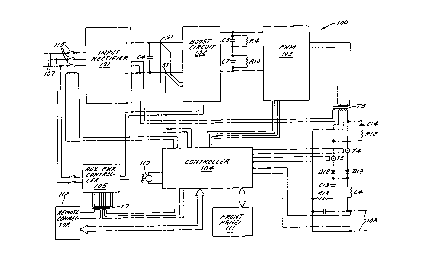
Figure 1 is a block diagram of the preferred
embodiment of the present invention;
F~gure 2 is a detailed diagram of the inputrectifier of Figure l;
Figure 3 is a detailed diagram of the boost
circuit of Figure 1;
Figure 4 is a detailed diagram of the pulse
width ~AlllAtor of Figure l; and
Figure S is a control circuit for the auxiliary
power ~ LLoller of the present invention.
-
D~TATrl~n DF~CRIPTTON OF T~ ~n EMBODIMENT
Referring now to Figure 1, the welding power
source 100 includes an input rectifier 101, a boost
circuit 102, a pulse-width modulator 103, a controller
104, an al~y~ ry power controller 105, a pair of storage
capacitors C3 and C7, and their associated protective
resistors R4 and R10, an output transformer T3, an output
inductor L4, feedbac~ current transformers T4 and T6,
feedback capacitors and resistors C13, C14, R12 and R13,
and output diodes D12 and D13 to provide a welding ouL~uL
current on welding output terminals 108. A cooling fan
110, a front panel 111, and a remote connector 112 are
also shown schematically.
In operation, power source 100 receives a
three-phase line voltage on input lines 107. The three-
phase input is provided to input rectifier 101. Input
rectifier 101 rectifies the three-phase input to provide
a generally dc signal. A 10 microfarad capacitor c4 is
- 216~6~
-- 7
provided for high frequency decouplinq of the boost
circuit. The dc signal has a magnitude of approximately
1.35 times the magnitude of the three-phase input. The
decoupled dc bus is provided to boost circuit 102. As
will be described in greater detail below, boost circuit
102 processes the dc bus provided by input rectifier 101
to provide a dc ouL~uL voltage having a co..Llollable
magnitude. In the preferred emho~iment the output of
boost circuit 102 will be approximately 800 volts,
regardless of the input voltage.
The ouL~uL of boost circuit 102 is provided to
pulse-width modulator 103, where the dc bus is inverted
and pulse-width modulated to provide a collLLollable
signal suitable for transforming into a weldinq output.
Controller 104 is a main control board such as that found
in many inverter-type welding power sources. The main
cG,lLLol board provides the control signals to pulse-width
modulator 103, to co.l~.ol the frequency and pulse-width
of pulse-width modulator 103. Input rectifier 101,
- pulse-width mo~ tor 103, ~Gl,L~oller 104 and output
transformer T3 are well known in the art.
The ouL~uL of pulse-width modulator 103 is
pro~ided to an o~L~uL transformer T3, which, transforms
the o~L~uL of PWM 103 to provide a voltage and current
suitable for welding. Transformer T3 has a center tap
secondary and is provided with a turns ratio of 32 turns
on the primary to 5 turns on each half for the center tap
secondary. Of course, other transformers may be used.
The alternating o~L~u~ of transformer T3 is rectified and
smoothed by an output inductor L4 and ouL~L diodes D12
and D13. Inductor L4 has an inductance sufficient to
provide desirable welding characteristics, such as, for
example, in a range of 50-150 microhenrys.
Auxiliary power controller 105 receives the
input line voltage and converts that voltage to a 18 volt
dc control signal. The 18 volt control signal is created
regardless of the input voltage, and is provided to boost
circuit 102. Boost circuit 102 uses the 18 volt control
- -; 2~60866
_ -- 8
signal to control its switching frequency and the
magnitude of its output. Auxiliary power controller 105
also provides a 48 volt center tap ac power signal to
con~oller 104.
- 5 Front panel 104 is shown schematically and is
used to col~ey operating status to the user, as well as
receive inputs as to operating parameters. Similarly,
remote co~Pctor 112 is shown schematically and is used
to receive inputs as to operating-parameters.
Generally spP~king, at power-up a three phase
input is provided on input lines 107. A plurality of
initially open contactors 115 isolates the input power
from input rectifier 101. However, the input power is
provided to auxiliary power controller 105. As will be
described in greater detail below, a~Yi~i~ry power
co,l~oller 105 determines the magnitude of the input
power, and opens or closes a number of contacts to
provide a 48 volt center tap ac GuL~uL to ~orl~Loller 104,
regardless of the input. The contacts are closed and
Z0 opened in~such a way as to provide safeguards against
underestim~ting the magnitude of the input voltage, and
thus protecting the circuit compo~ents. Also, al~ ry
power cGl.LLoller 105 provides an 18 volt dc control
signal to boost circuit 102, regardless of the magnitude
of the input.
After the voltage level has been properly
determined by closing the proper contacts eG,.Lloller 104
causes contacts 115 to be closed, thus providinq power to
input rectifier 101. Input rectifier 101 includes a
precharge circuit to prevent a resonant overcharge from
harming capacitors C3 and C7 and to avoid P~P~ively
loading of the input source. A signal received by input
rectifier 101 from a tap on transformer T3 turns on an
SCR (described in more detail below). The conducting SCR
bypasses input current around the precharge resistors.
The ou~ of input rectifier 101 is provided
to boost circuit 102. Boost circuit 102 is well known in
the art and integrated circuit controllers for boost
2i6~856
circuits may be purchased commercially. In operation
boost circuit 102 senses the voltage at its inputs and
its outputs. As will be described in more detail later
and IGBT (or other switching element) is switched on and
off at a frequency and duty cycle (or pulse width) to
obtain a desired output voltage. In the preferred
embodiment the desired o~L~L voltage is approximately
800 volts.
Boost circuit 102 thus provides an o~L~uL of
about 800 volts to 800 microfarad electrolytic capacitors
C3 and C7, which have 45K ohm bleeder and balancing
resistors R4 and R7 associated therewith. Capacitors C3
and C7 thus acts as a dc link for PWM 103.
PWM 103 receives a generally constant 800 dc
signal and mo~t~l~tes it to provide, after transformation,
rectification and smoothing, a welding ouL~uL at a user
selected magnitude. PWM 103 modula~es its input in
accordance with col.~.ol signals received from cul,LLoller
104. PWM 103 also receives a 25 volt dc power signal
from ~o..L~oller 104. Such a PWM is well Xnown and PWM
103 may be purchased commercially as a single module.
The ~ uL of PWM 103 is provided to output
transformer T3 and which transforms the relatively high
voltage, low current signal to a voltage suitable for use
in welding. The o~L~uL of transformer T3 is rectified by
diodes D12 and D13, and smoothed by output inductor L4.
Thus, a generally constant magnitude dc welding u~L~uL is
provided on welding o~L~uLs 108.
Current transformers T4 and T5, provide
feedback signals to controller 104, cnllhh~r capacitors
C13 (0.1 microfarads) and C14 tO.022 microfarads), and
snubber resistors R12 (12 ohms) and R13 (47 ohms)
suppress voltage transients associated with recovery of
D12 and D13. Controller 104 compares the feedback
signals to the desired welding current, and appropriately
controls PWM 103 to adjust its switching pulse width if
necessary.
- 2~ 6086~
.
-- 10 --
Referring now to Fi~ure 2, the preferred
embodiment for input rectifier 101 is shown in detail and
includes a full wave bridge ccmprised of diodes D4, D5,
D6, D9, D10 and D11. The bridge rectifies the three
phase input to provide a signal having a magnitude of
about 1.35 times the input voltage magnitude. A pair of
50 ohm resistors R1 and R2 are provided to precharge
capacitors-C4, C3 and C7 (shown in Figure 1) upon start
up. This prevents a sudden surge of current ~rom being
dumped into capacitors C4, C3 and C7.
After the precharge is completed an SCR Ql is
turned on via a signal from a tap on o~uL transformer
T3 (also in Figure 1). The signal from transformer T3 is
provided to the gate of SCR Ql via a ~LLe~lL limiting
resistor R6 and capacitor C6. A reco~eL~ diode D7 and
~nuhh~r resistor R5 are provided across the gate of SCR
Ql. SCR Ql shunts the resistors and allows the maximum
current flow to inductor L2 of boost circuit 102.
A plurality of varistors RVl-RV3 are provided
to ~ ass line spikes. Additional varistors (not
shown) may be provided between D9-Dll and ground to
further ~ L eSS spikes.
As one skilled in the art will readily
rec~ nize, other circuits and circuit elements will
accomplish the function of input rectifier 101.
Referring now to Figure 3, the details of one
embodiment of boost circuit 102, which operates in a
manner well known in the art, is shown. Generally
speaking, boost circuit 102 provides an o~L~uL voltage
that is equal to the input voltage divided by one minus
the duty cycle of a switch IGB~l in boost circuit 102.
Thus, if the switch IGBTl is off 100% of the
time the ouL~uL voltage (the dc link voltage) is equal to
the input voltage (from capacitor C4 and input rectifier
101). In one embodiment the lowest input is about 200
volts, and the desired output (dc link voltage) is 800
volts, thus-the upper limit for the ~boost~ is about
400%, and requires a duty cycle of about 75%.
216~866
The operation of a boost circuit should be well
known in the art and will be briefly described herein.
When switch IGBTl is turned on, current flows through an
inductor L2 to the negative voltage bus, thus storing
energy in inductor L2. When switch IGBT1 is subsequently
turned off, the power is returned from inductor L2
through a diode Dl and a 14 microhenry saturable-reactor
L1 to the dc link. The amount of energy stored versus
~eL~.ed is controlled by controlling the duty cycle in
accordance with the formula stated above. In order for
the boost circuit to operate properly inductor L2 must
have continuous current, therefore inductor L2 should be
chosen to have a large enough inductance to have a
continuance current over the range of duty cycles. In
one ~ho~; ment inductor L2 is a 3 millihenry inductor.
The remaining elements of boost circuit 102 include a
0.0033 microfarad capacitor Cl, a diode D3, a 1 ohm
resistor R3, a 50 ohm resistor R6, a diode D8, a 50 ohm
resistor R7 and a 0.1 microfarad capacitor C8 which are
20~ primarily ~ hhers and help the diode recover when switch
IGBT1 is turned on.
Boost circuit 102 includes an IGBT driver 301
that controls the duty cycle of switch IGBT1. Driver 301
receives feedback signals indicative of the output
voltage and the input current, and utilizes this
information to drive switch IGBT1 at a duty cycle
sufficient to produce the desired ouL~uL voltage.
In one embodiment, boost circuit 102 includes a
shunt S1 (shown on Figure 1). Shunt Sl provides a
feedback signal that is the current flowing in the
positive and negative buses. A Unitrode power factor
correction chip is used to implement boost circuit 102 in
the preferred emho~;ment and requires average current
flow as an input. In response to this information and
the dc link voltage, driver 301 turns switch IGBT1 on and
off.
- 216086~
-
- 12 -
As one skilled in the art will readily
recognize, other circuits and circuit elements will
accomplish the function of boost circuit 102.
As stated above, the output of boost circuit
102 is provided to capacitors C3 and C1 (Figure 1) and is
the dc link voltage. In one embodiment the dc link
voltage is 800 volts, as determined by the switching of
switch IGBTl. In the preferred embodiment, using the
component values described herein the dynamic regulation
of the dc link voltage is 80 volts from full load to no
load. Static regulation is about a +/-2 volts, with a
ripple of about +/-20 volts.
The dc link voltage is provided to pulse width
modulator 103. PWM 103 is a st~ rd pulse with
lS modulator and provides a quasi-square wave o~L~uL having
a magnitude equal to the magnitude of the input, as would
any other PWMs. Thus, the o~L~L of PWM 103 is about
+400 volts to -400 volts for an 800 volt peak to peak
centered about zero.
- PWM 103 includes a pair of switches Q3 and Q4
(prefera~ly IGBTs) and a pulse width driver 401. Driver
401 receives feedback from current transformers T1 and
T2, and receives control inputs from controller 104. In
response to these inputs driver 401 provides gate signals
to switches Q3 and Q4, thereby modulating the input
signal. A capacitor C2 (4 microfarad) a capacitor C9
(4 microfarad) are provided between the dc link and the
ouL~uL transformer T3. A capacitor C5 (0.0022
microfarad), resistor R11 (50K ohm) and resistor R9 (SOX
ohm) are snubber circuits.
As one skilled in the art will readily
recognize, other circuits and circuit elements will
accomplish the function of PWM 103.
The o~L~uL of PWM 103 is provided to
transformer 103, and the current in transformer 103 is
determined by the modulation of PWM 103. As stated
above, the output of transformer T3 is rectified by
diodes D12 and D13 and is smoothed by inductor L4. The
- ~16~866
dc output current is fairly flat; the ripple at full load
(300 amps) is about 12 amps peak to peak. At full load
the duty cycle of each switch Q3 and Q4 of PWM 103 would
be about 20-35% (40-70% overall duty cycle).
In an alternative embodiment the ouL~uL of PWM
103 may be rectified ~y other output rectifiers such as a
synchronous rectifier (cycloconverter) that provides an
ac ouL~L signal at a frequency less than or equal to the
frequency of the output of PWM 103. Other o~LpuL
circuits, including inverters, that provide a welding
current may also be used.
Referring again to Figure 1, oo~.LLoller 104 is
connected to current transformers T4 and T5, which
provide feedbac~ information. Controller 104 receives
lS power from auxiliary power controller 105 and provides as
one of its ou~uL the driver control for the PWM driver.
It also includes an over voltage protection sense which
monitors the voltage coming out of input rectifier 101.
If the voltage from input rectifier 101 is dangerously
~0 high controller 104 causes contactors 115 to open, to
protect circuit ~r~nents. According to one embo~im~t
930 volts dc is the cut off point for what is considered
to a dangerously high voltage.
As may be seen from the above description,
welding power source 100 receives an input voltage and
provides a welding ouL~uL. Regardless of the magnitude
of the input voltage boost circuit 102 boosts the input
voltage to a desired (800 volts e.g.) level. Then PWM
103 modulates the signal to provide an appropriate level
of power, at 800 volts, to transformer T3.
The above arrangement is satisfactory for any
input voltage, however, there must be some mechanism to
provide control voltages at the proper level. As will be
described below, auxiliary power controller 105 performs
that function, and the embodiment thereof is shown
schematically in Figure 5.
With re-ference now to Figure 5, a plurality of
connectors Jl, J2, J3 and J4 are shown. An 18 volt dc
- 216086~
- 14 -
control voltage output is provided on connector J1 to
boost circuit 102 (shown on Figure 1). As will be
described in greater detail below, the 18 volt dc control
signal is provided regardless of the magnitude of the
S - input voltage. Connector ~2 feeds power bac~ to
auxiliary power controller 105 for internal use.
Conn~ctor J3 connects the input ac voltage to appropriate
taps on a transformer T7 (Figure 1) to provide a 30 volt
ac signal to remote ~o~nector 112 (Figure 1). Similarly,
a 48 volt center tap ac signal is provided to col,LLoller
104. Controller 104 uses the 48 volt center tap ac
signal to generate dc control signals and to power fan
110. Connector J4 of auxiliary power ~o"L~oller 105 is
connected via a user controlled on/off switch S4 to the
input power lines (Figure 1).
Auxiliary power controller 105 controls the
connections to taps on the primary of an auxiliary power
transformer T7. Transformer T7 is a 200 VA transformer
whose primaries are co~n~cted to al~Y;li~ry power
controller 105 as described above with reference to
co~nPctor J2 and J3. Se~eral taps on its secondary are
connected to ~ L oller 104 and the rP~ining secondary
taps are connected to remote connector 112.
. Referring again to Figure 5, the taps on J3 are
associated with the following voltages: 575, 460, 380,
230 volts, and the LeL~ 1l, beginning at the uppermost tap
and pro~ ing downward. As will be described below,
when a~ ry power controller 105 selects the
appropriate tap for a given input voltage, transformer T7
3 0 will provide a 48 volt center tap ac signal on its
secondary for use by controller 104.
As may be seen on Figure 5, the ac input is
received on connector J4 and provided (via a fuse Fl, and
a pair of 4 . 7 ohm resistors R18 and R19) to a series of
relays K2B, KlB, K3C and K3B that determine the tap on
connector J3 selected for the output. When 575 volts are
present at the input relays K2B and K3C should be to the
right. Then the input is connected across the upper and
--- 216086~ -
-- 15 --
lower most taps on connector J3. These taps are
connected to the appropriate taps on transformer T7 such
that the output of transformer T7 that is provided to
controller 104 is approximately 48 volts center tap when
S 575 volts are provided to the primary of transformer T7.
When 460 volts are present at the input relay
K2B should be to the left, and relay KlB should be to the
right. ~This connects the ac input to the second
uppermost and the lowest taps on connector J3 The
remaining voltages are similarly accommodated. A pair
O.lS microfarad capacitors C13 and C14 are provided for
snubbing and spike suppression as the primaries of
transformer T7 are switched.
In operation the circuitry on the left side of
Figure 5 determines the input voltage, and sets the
relays for that voltage. At start up the relays are as
shown in Figure 5 and are suitable ~or an input voltage
of 575 volts. Because this is the highest possible input
voltage, all components will be protected, i.e. either
the voltage is properly selected, or the input voltage is
less than the cu~o~lent design capabilities. If
auxiliary power controller lOS determines that 575 volts
are in fact present, the relays will remain as shown.
However, if auxiliary power co..L,oller 105 determines
that less than 575 volts are present, the state of relay
K2B will be changed (to be to the left), so that the
o~ L is appropriate for a 460 volt input.
This process is repeated, always stepping down
to the next highest voltage, until the appropriate input
voltage is sensed. In this manner the components in
controller 104 will be protected from a dangerously high
voltage being applied to controller 104.
The voltage for sensing is provided to
auxiliary power controller loS via connector J2, which is
connected to secondary taps on transformer T7. Thus, if
the tap selected on connector J3 was not correct, then
the voltage on connector J2 will be too low, and
auxiliary power controller loS will select the
- ` ~160866
- 16 -
appropriate relay setting to step down to the next
voltage level. As stated above, the stepping down
continues until the proper vsltage is sensed on connector
J2.
S The input from connector J2 is provided to a
rectifier comprised of diodes CR1, CR2, CR3 and C~4.
These diodes rectify the ac signal and provide it to a
pair of 220 microfarad smoothing capacitors C1 and C2.
The rectified voltage is +/-18 volts dc if the proper tap
on co~n~ctor J3 is selected. If the incorrect tap is
selected the voltage will be less than +/-18 volts, but
will be referred to as nominally +/-18 volts. The
nominal +/-18 volt supply is provided at other locations
throughout the auxiliary power controller 105 circuit,
including to a 30 volt zener diode CR7, used to determine
if the proper tap on connector J3 has been selected.
At~ili Ary power controller 105 determines if
575 volts is present on the input using the following
comron~nts: zener diode CR7, a 10 microfarad capacitor
-Cg, a pair of gates U2B and U2C configured as darlington
drivers for a winding K2A of relay K2, a lOK ohm resistor
RN2A, a lOK ohm resistor RN2B, a 820 ohm resistor R9, and
a diode U3B. Gates U2B and U2C are also used as sensing
devices and have a threshold of about 4 volts (relative
to their reference voltages) on the input (pin 1) of gate
U2B pin 1.
Initially, gate U2B has a LOW output and is
referenced to nominal -18 volts. Gate U2B will not
switch states so long as the input is at least 4 volts
greater than its reference voltage (nominally -18 volts
relative to ground). In operation the nominal +18 volts
will be provided to diode CR7 and the nominal -18 volt
signal is applied to a 10 microfarad capacitor C9. As a
result of the 30 volt zener drop, the input to gate U2B
3S will be at -12 volts (relative to ground) if the proper
tap has been selected. If 575 volts are present at the
input, there will be 6 volts relative to the reference
voltage (-18 volts) at the input to op amp U2B, and the
-. - 2~60866
.
output state of gate U2B will remain low. So long as the
output of U2B r~i n~ low the current will not flow in
the winding of relay K2 and relay K2B will remain as
shown in Figure 5.
However, if only 460 volts are present on the
input and the relays are as shown in Figure 5 (as they
will be at power up), then the nominal ~/-18 volts will
actua~lly be +/-14.4 volts. Thus, 28.8 volts are applied
across zener diode C~7 and capacitor C9. GiYen the 30
volt zener drop, -14.4 volts will be applied to the input
of gate U2B. Because this is also the reference voltage
for gate U2B, the threshold is crossed, and the o~L~u~ of
gate U2B will change states. Current will then flow in
the wi~ g of relay X2 and relay K2B will change states,
configuring the J3 taps for 460 volts. If less than 460
volts is present at the input the same result will occur.
The sensing and stepping down to 380 volts and
230 volts occur in a similar manner using similar
components. Referring to Figure 5, the sense and step
- 20 down circuit to 380 volts include a 100 ohm resistor R17,
a pair of lOK ohm resistors RN2C and RN2D, an 820 ohm
resistor R8, a diode U3C, a 10 microfarad capacitor C6, a
pair of gates U2D and U2E, and a winding KlA for relay
Kl. A relay K2C is provided to prevent relay Kl from
changing states before the step down to 460 volts occurs.
In the manner described above with respect to the step
down to 460 volts, the current will be provided to
winding KlA of relay Kl if less than 460 volts is
provided at the input. This will cause relay KlB to move
to the left position and connect the tap on J3 associated
with a 380 volt input.
The circuitry associated with the step down to
230 volts includes a 100 ohm resistor R16, a pair of lOK
ohm resistors RNlA and RNlB, an 820 ohm resistor R11, a
diode U3E, a pair of gates U2F and U2G, a winding K3A for
relay K3, relay KlC, diode CR5 and zener diode CR4. A
relay KlC is provided to prevent relay K3 from changing
states before the step down to 380 volts occurs. The
- ` 2160866
- 18 -
step down to 230 volts operates in the same manner as the
step down to 380 volts and 460 volts as described above.
If less than 380 volts is applied on the connector J4
inputs, gates U2F and U2G will cause current to flow
~hrough wi ~; ng K3A of relay K3. This will cause reiay
~3B to move to the left and connect the tap on J3 for 230
volts to the ac input.
~hus, as may be seen from the above
description, the circuitry of auxiliary power controller
lOS senses the ac input voltage and co~ects the
a~Lo~iate tap on the auxiliary power transformer T7 to
the ac input voltage. As may be seen from the above
~icc~1~cion~ this is done in a manner which protects
co~onents by assuming the voltage is, upon start up, the
highest possible voltage. If the voltage is less than
the highest possible voltage, the next lowest voltage
will then be assumed. This process is repeated until the
actual voltage is ob~
In the event that the ac input is 230 volts, at
start up there will not be sufficient power from the
nominal +/- 18 volt signal to drive the relays because
the tap associated with 575 volts on connector J3 is
selected at start up. To compensate for this, circuitry
that boosts the voltage supplied on connector J2 is
provided. This circuitry includes a 1 millihenry
inductor Ll, a switch Q4, a timer Ul, a switch Q2, a
switch Q1, and a switch TIP120. Also included are
associated circuitry including a 22 ohm shunt resistor
R13, a lK resistor R5, a lOK resistor R12, a lOK resistor
R14, a 2.2K resistor R4, a lK resistor R6, a lK resistor
R2, a 20K resistor R3, a 220 ohm resistor R7, a lOK
resistor RNlD, a 4.7K resistor R10, a 470 picofarad
capacitor C4, a .oOl microfarad capacitor C3, a 0.1
microfarad capacitor CS, a 220 microfarad capacitor Cll,
3S a 220 microfarad capacitor C12, a diode cR12, a diode
CR8, a zener diode CR10, a diode CR5, and a zener diode
CRll.
` 2160866
The boost power source circuitry operates as a
typical boost circuit. The boost is provided by inductor
Ll and switch Q4. During the time switch Q4 is ON,
current flows through inductor Ll, shunt resistor R13 and
switch Q4 to the negative voltage supply. During this
time, energy is stored in inductor L1. When switch Q4 is
OFF, the energy stored in inductor L1 is Le~uL~ied to the
positive voltage supply (+B) through diode CR12. By
appropriate timing of the turning ON and OFF of switch
Q4, a desired voltage may be obtained. Timer chip Ul is
used to provide the ON/OFF gate signals to switch Q4 and
is an LM555 timer. When the voltage on resistor R13
becomes sufficiently hiqh, it will trip the input on U1,
which in turn will cause the output of timer U1 to turn
switch Q4 OFF.
Initially, switch Q4 is in the ON position and
current increases and eventually reaches the point where
the voltage on resistor R13 is sufficiently high to trip
the threshold on timer U1 through resistor R12. Thus,
switch Q4 will remain ON for a length of tLme sufficient
to build up enough enerqy to, when it is turned OFF,
raise the nominal +/- 18 volts to a level sufficient to
drive the relays.
Switches Q2 and Q1 enable or disable timer U1
when the taps on connector J3 are such that the nominal
+/- 18 volt signal is actually +/- 18 volts. When switch
Q2 is turned OFF, timer U1 is disabled through its VCC
input. Also, switch TIP120 is a linear regulator. When
the nominal +18 volt supply is insufficient to drive the
relay, switch TIP120 will provide the boost source to
drive the relays. When the nominal +~8 voltage is
sufficient to drive the relay, switch Q2, timer U1 and
switch Q4 are turned off. The +18 volt supply is coupled
through L1 and CR12 to regulator TIP120; the +B boost
supply is then fed directly by the sufficiently high +18
volt supply. The TIP120 regulator regulates relay supply
at 24 volts relative to the ~ volt supply.
-18 J,z~
` 2160866
- 20 -
In addition to the circuitry above, circuitry
is provided that protects in the event of an overvoltage.
This circuitry includes a switch Q5, a gate U2A, a lO0
ohm resistor Rl5, a lOK ohm resistor RN3A, a lOK ohm
resistor ~.3B, a lOK ohm resistor RN3C, a lO microfarad
capacitor C10, diodes CRl4 and U3H, and lO volt zener
diode CR13. An overvoltage occurs when the tap selected
on connector J3 corresponds to a voltage less than the
voltage at the ac input. This may occur when either the
incorrect tap has been selected or when a temporarily
high voltage is provided at the ac input.
In the event an overvoltage occurs, the voltage
at the node common to diodes CR13 and CR7 will rise to a
voltage greater than 14 volts with respect to the nn~
-18 volt signal. This causes the low side of diode CR13
to be greater than 4 volts with respect to the nominal -
18 volt signal, and the input of U2A will change from an
input low state to an input high state. When the input
of U2A changes from low to high, the o~L~uL will change
from an o~L~ L high state to an ouL~uL low state. The
ouL~L low state of U2A will bring the relay supply
voltage to a virtual 0 through diodes U3~ and CRl4. This
causes the relays to return to the state shown in Figure
2, which ac~ oA~tes the highest voltage possible (575
volts). At that time the previously described tap
selection process stepping from the 575 to 460 to 380 to
230 taps begins again until the correct tap is selected
to match the input voltage received on connector J4.
Accordingly, the components of controller 104 will be
protected.
Other modifications may be made in the design
and arrangement of the elements discussed herein without
departing from the spirit and scope of the invention as
expressed in the appended claims.