Note: Descriptions are shown in the official language in which they were submitted.
~~.. f~ .~
1
TITLE OF THE INVENTION:
A Compact Diversity Antenna with Weak Back Near
Fields
NAME i(,S ) OF INVENTOR Q S )i
Ronald H. Johnston
Laurent Joseph Levesque
FIELD OF THE INVENTION
This invention relates to diversity antennas that
can simultaneously receive or transmit two or three
components of electromagnetic energy.
BACKGROUND OF THE INVENTION
Antenna diversity is especially useful for
improving radio communication in a multipath fading
environment. Sporadic deep fades occur (especially in an
urban or inbuilding environment ) on a radio channel leading
to signal loss. Without diversity, power levels must be
maintained sufficiently high to overcome these deep fades.
Antenna diversity may be used to produce low correlation
radio channels which produce signal amplitudes that are
statistically independent. The probability of simultaneous
deep fades on uncorrelated channels is relatively low.
When a deep signal fade occurs on one channel, signal
degradation or loss can usually be avoided by switching to
another channel. Consequently, signal reliability can be
improved, and power requirements can be reduced while
maintaining signal reliability by using antenna diversity.
The improvements in signal strength with various diversity
antenna combining techniques are quantified by authors such
as W.C. Jakes, Editor, Microwave Mobile Communications,
2
IEEE Press, pp. 309-329,1994, and W.C.Y. Lee, Mobile
Communications Engineering, McGraw-Hill, pp. 291-318, 1982.
Increasing the number of diversity channels
improves signal reliability and lowers the transmitter
power requirement. However, as the number of diversity
channels is increased, the incremental improvement
decreases with each additional diversity channel. For
instance, two-way diversity offers a significant
improvement over a single channel. Three-way diversity
offers a significant improvement over two-way diversity,
although the incremental improvement is not as great. At
higher diversity levels, i.e., greater than 5, the signal
improvement is generally not significant when weighed
against the additional complexity of the switching and
control circuitry. Three-way diversity can significantly
improve signal to noise ratio over two-way diversity, but
neither are widely used, largely, it is believed, due to a
lack of antennas with suitable compactness, bandwidth and
ruggedness.
There are several types of antenna diversity.
Angle diversity involves the use of elemental antennas with
narrow beams that point in slightly different directions.
Sufficient angle separation between the elemental antennas
produces low correlation channels. Space diversity
involves separating antennas by a sufficient distance
(horizontally or vertically) to produce low correlation
channels. These two methods have the disadvantage of
requiring separate antennas and are generally not
physically compact.
Polarization diversity involves having elemental
antennas for independently receiving separate polarizations
of the electromagnetic wave. Channels may exhibit
sensitivity to the polarization of the transmitted
electromagnetic wave.
3
E.N. Gilbert, "Energy Reception for Mobile
Radio", BSTJ, vol. 44, pp. 1779-1803, October 1965, and
W.C.Y. Lee, Mobile Communications Engineering, McGraw-Hill,
pp. 159-163, 1982 have proposed a field diversity antenna
where three individual antennas are sensitive to Hx, Hy and
Ez field which are all vertically polarized. Pattern
diversity uses broad radiation patterns of elemental
antennas to receive or transmit into wide angles but each
elemental antenna has a different arrangement of nulls to
suppress multipath fading effects. Pattern, polarization
and field diversity methods are probably the most promising
for producing compact diversity antennas. T. Auberey and
P. White, "A comparison of switched pattern diversity
antennas", Proc. 43rd IEEE Vehicular Technology Conference,
pp. 89-92, 1993, have shown that the Hx, Hy and Ez field
diversity antenna has very similar performance to the three
way pattern diversity with patterns of sin ~, cos ~ and
omni.
It has recently been shown that standard cell
phone antennas deposit between 48~ and 68~ of transmitter
output energy into the head and the hand of the user, M.A.
Jensen and Y. Rahmat-Samii, "EM Interaction of Handset
Antennas and a Human in Personal Communications", Proc.
IEEE, Vol. 83, No. 1, pp. 7 - 17, January, 1995.
This deposition of electromagnetic energy (into
the head especially) raises health and legal issues and it
also removes EM power from the communications channel. It
therefore behooves the antenna designer to find methods for
reducing this electromagnetic energy deposition into the
head of a cell phone user.
A moderate number of diversity antennas are
discussed in the literature as reviewed by R.H. Johnston,
"A Survey of Diversity Antennas for Mobile and Handheld
4
Radio", Proc. Wireless 93 Conference, Calgary, Alberta,
Canada, pp. 307-318, July 1993.
Three of the antennas discussed in that paper
should be considered in relation to the three way diversity
antenna being presented here. These are:
The crossed loop antenna of E.N. Gilbert, "Energy
Reception for Mobile Radio" BSTJ, vol. 44, pp. 1779-1803,
October 1965, and W.C.Y. Lee, Mobile Communications
Engineering, McGraw-Hill, pp. 159-163, 1982, responds to
the Hx, Hy and Ez radiation fields. The antenna requires
three hybrid transformers which introduce circuit
complexity and signal power loss and the antenna requires
a large ground plane. The issue of antenna efficiency,
impedance matching and bandwidth are not effectively
addressed.
The slotted disk antenna of A. Hiroyaki, H.
Iwashita, N. Taki, and N. Goto, "A Flat Energy Diversity
Antenna System for Mobile Telephone", IEEE Transactions on
Vehicular Technologies, Vol. VT40, no. 2, pp. 483-486, May
1991, also responds to the Hx, Hy and Ez fields and is an
innovative and complete design with a diameter of about
0.6~, and a height of about 0.05, and has bandwidths of 10~
and 6~. The antenna has an interelemental antenna
isolations of lOdB. This antenna is the smallest antenna
presently available but even smaller sized antennas and
greater interelemental antenna isolations are required in
many cellular radio applications.
The multimode circular patch antenna by R.G.
Vaughan and J.B. Anderson, "A Multiport Patch Antenna for
Mobile Communications", Proc. 14th European Microwave
Conference, pp. 607-612, Sept. 1984, provides approximately
a sin ~, cos ~ and omni radiation pattern but the antenna
is fairly large and the isolation is only about lOdB. The
~.~ ~~~2
antenna is a microstrip patch design which is inherently
narrow band for a reasonable dielectric thickness.
H.A. Wheeler, in a paper entitled "Small
Antennas", IEEE Transactions on Antennas and Propagation",
5 Vol. AP-23, no. 4, pp. 462-469 (Fig. 12), July 1975,
discusses a structure which has an appearance similar to
one of the embodiments seen later in this patent
application. It shows an open top shallow square box with
cross conductors across the top. Wheeler indicates that
this antenna has good bandwidth for its size and it may be
operated in two modes. He does not note that this can
provide diversity operation and he does not note the
possibility of the third vertical elemental antenna which
produces another mode of operation.
The standard antennas used on handheld cellular
radio telephones are the electric monopole mounted on a
conductive box and single and double PIFA (Planar inverted
F antennas) and BIFA (Bent inverted F antennas) mounted on
conductive boxes. Recent analytical work on these antennas
indicate that these various antennas deposit between 48~
and 68~ of the total output power into the head and the
hand of the user, M.A. Jensen and Y. Rahmat-Samii, "EM
Interaction of Handset Antennas and a Human in Personal
Communications", Proc. IEEE, Vol. 83, No. l, pp. 7-17,
January, 1995.
StJI~IARY OF THE INVENTION
In a broad aspect of the invention, there is
therefore provided an antenna comprising:
means forming a ground plane;
a first antenna element extending in a loop from
a first part of the ground plane to a second part of the
ground plane; and
~~k~~2
6
a second antenna element extending in a loop from
a third part of the ground plane to a fourth part of the
ground plane, the second antenna element intersecting the
first antenna element at an intersection.
In a further aspect of the invention, a third
antenna element forming a conducting monopole having a
predominantly Ez field radiation pattern is located at the
intersection of the first and second antenna elements.
In a further aspect of the invention, there is
provided feed means to feed electric signals to the first
and second antenna elements. The feed means is configured
to produce a virtual ground at the intersection of the
first and second antenna elements, thereby providing
isolation of the antenna elements.
In a further aspect of the invention, the feed
means provides feed electric signals to the first and
second antenna elements at the intersection of the first
and second antenna elements.
In a further aspect of the invention, the ground
plane forms a box, the box including a peripheral wall
depending from the first and second antenna elements and a
bottom spaced from the first and second antenna elements
and enclosed by the peripheral wall.
In a further aspect of the invention, each
antenna element is formed of strips whose width is greater
than their thickness.
In a further aspect of the invention, the first
and second antenna elements bisect each other.
In a further aspect of the invention, the ground
plane is commensurate in size to the first and second
antenna elements.
In a further aspect of the invention, each of the
first and second antenna elements is curved.
7
In a further aspect of the invention, each of the
first and second antenna elements form part of a spherical
shell.
In a further aspect of the invention, the ground
plane extends laterally no further than the first and
second antenna elements.
In a further aspect of the invention, the first
and second antenna elements extend between diagonal corners
of the box.
In a further aspect of the invention, the first
and second antenna elements are orthogonal to each other.
In a further aspect of the invention, at least
each of the first and second antenna elements create a
reactance in use and the invention further includes means
integral with each of the first and second antenna elements
for tuning out the reactance of the respective first and
second antenna elements.
In a further aspect of the invention, each means
for tuning out the reactance of the first and second
antenna elements includes a capacitative element matching
the respective one of the first and second antenna elements
to a given impedance.
In a further aspect of the invention, the feed
means for each antenna element forms a transmission line
connected to the respective antenna elements at the
intersection of the antenna elements.
In a further aspect of the invention, the feed
means includes, for each antenna element, a conducting
microstrip capacitatively coupled to the antenna element.
In a further aspect of the invention, the first
and second antenna elements are each formed of first and
second conducting strips spaced from each at the
intersection of the first and second antenna elements; and
~~.~~.~~2
8
the conducting microstrip of each antenna element
connects to one of the first and second conducting strips
and extends along and spaced from the other of the first
and second conducting strips.
In a further aspect of the invention, the feed
means for each antenna element is a coaxial transmission
line in which an outer conductor is continuously connected
to a portion of the antenna element.
In a further aspect of the invention, the feed
means includes a first feed point on the first antenna
element, a second feed point on the second antenna element,
a source of electrical energy, and a splitter connected to
the source of electrical energy and to the first and second
feed points to provide equal anti-phasal currents to the
respective first and second feed points.
In a further aspect of the invention, there is
provided a mobile phone transceiver comprising a housing,
a radio transceiver disposed within the housing, the
radiotransceiver including a microphone on one side of the
housing; and an antenna having means forming a ground plane
with a weak near field on a first side of the antenna, and
antenna elements on a second side of the antenna, the
antenna being oriented with respect to the housing such
that when the microphone is in position close to the mouth
of a mobile phone user the first side of the antenna is
closer to the head of the user than the second side of the
antenna.
These and other aspects of the invention will now
be described in more detail and claimed in the claims that
follow.
BRIEF DESCRIPTION OF THE DRAWINGS
There will now be described preferred embodiments
of the invention, with reference to the drawings, by way of
~~.~ ~~~~
9
illustration, in which like numerals denote like elements
and in which:
Fig. 1 is a schematic showing arrangement of two
magnetic loops and one electric monopole according to an
aspect of the invention;
Fig. 2 is a schematic showing an embodiment of
loop conductors lying on the surface of a spherical shell
according to an aspect of the invention;
Fig. 3 is a schematic showing a rectangular
conductor top view embodiment according to an aspect of the
invention
Fig. 4 is a schematic showing a square ground
plane according to an aspect of the invention;
Fig. 5 is a schematic showing a round ground
plane according to an aspect of the invention;
Fig. 6 is a schematic showing a diamond shaped
ground plane according to an aspect of the invention;
Fig. 7 is a schematic showing a non-symmetrical
rectangular ground plane according to an aspect of the
invention;
Fig. 8 is a schematic showing an embodiment using
a local sunken ground plane according to an aspect of the
invention;
Fig. 9 is a schematic showing an embodiment of a
cylinder local sunken ground plane according to an aspect
of the invention;
Fig. 10 is a schematic showing an embodiment
installed in a conductive box according to an aspect of the
invention;
Fig. 11 is a schematic showing an embodiment on
top of a rectangular box structure according to an aspect
of the invention;
10
Fig. 12 is a schematic showing detail of
electrical feed points according to an aspect of the
invention;
Fig. 13 is a schematic showing a signal splitter
feed arrangement realized by a magic T according to an
aspect of the invention;
Fig. 14 is a schematic showing a signal splitter
realized by a 3dB Branch line coupler feed arrangement;
Fig. 15 is a schematic showing 3dB Splitter Feed
arrangement according to an aspect of the invention;
Fig. 16 is a schematic showing a feed arrangement
using a microstrip line feed according to an aspect of the
invention;
Fig. 17 is a schematic showing an equivalent
circuit of the magnetic loop elemental antennas according
to an aspect of the invention
Fig. 18 is a schematic showing a capacitive
matching circuit for the magnetic loop elemental antennas
according to an aspect of the invention
Fig. 19 is a schematic showing a T matching
circuit according to an aspect of the invention
Fig. 20 is a schematic showing a rr matching
circuit according to an aspect of the invention
Fig. 21 is a schematic showing a matching and
tuning circuit integrated with the loop antenna according
to an aspect of the invention
Fig. 22 is a schematic showing a detail of
individual H-Element electrical feed point according to an
aspect of the invention
Fig. 23 is a schematic showing the relationship
of the human head, antenna and cellular phone according to
an aspect of the invention;
Fig. 24 shows a pie shaped antenna configuration
according to an aspect of the invention;
~16~.8~~
1~
Fig. 25 shows a top view of the embodiment of
Fig. 24;
Fig. 26 shows a top view of a pie shaped antenna
configuration with diagonalized antenna loops;
Fig. 27 shows an embodiment of an antenna with
diagonalized pie shaped antenna elements for sliding over
a radio transceiver, such as shown in Fig. 23;
Fig. 28 shows a coaxial feed arrangement for an
antenna element according to an aspect of the invention;
Fig. 29a is a schematic showing basic components
of a first embodiment of a radio transceiver according to
the invention;
Fig. 29b is a schematic showing basic components
of a second embodiment of a radio transceiver according to
the invention; and
Fig. 30 is a schematic showing a feed for a
monopole antenna element for use in the invention.
DETAILED DESCRIPTION OF PREFERRED EMBODIMENTS
The three-way diversity antenna, as realized by
orthogonal horizontal conductors and a vertical conductor,
in a compact configuration, has many advantages over other
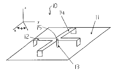
diversity antennas. One embodiment is shown in Figure 1.
The basic shape of the antenna 10 is shown without the
elemental antenna feed arrangements, and is formed on a
ground plane 11. The ground plane 11, and the other ground
planes shown in the figures, is preferably electrically
small, namely its length, in the longest dimension, should
be less than the wavelength, and preferably less than half
the wavelength, for example one-quarter of the wavelength,
of the carrier frequency of the transceiver the antenna is
to be used with.
The Hx antenna element 12 (aligned in the y
direction) extends in a loop from spaced apart locations on
~16~~~
12
the ground plane 11, provides (when a current passes
through it, that is, when it is in use) a magnetic field in
the x direction (Hx) which produces a vertically polarized
EM wave with approximately a sin ~ radiation pattern and
provides an electric field in the y direction, which in
turn produces a horizontally polarized EM wave with
approximately a cos ~ radiation pattern.
The Hy antenna element 14 (aligned in the x
direction) also extends in a loop from spaced apart
locations on the ground plane 11, and, in use, provides a
y directed magnetic field (Hy) which produces a vertically
polarized EM wave with an approximate pattern of cos ~ and
provides an electric field in the x direction (Ex) which
produces a horizontally polarized EM wave with
approximately a sin ~ radiation pattern.
This complete angular coverage and polarization
coverage makes the antenna very suitable for a cell phone
and personal communication phone as the antenna can have a
variety of orientations with the user and can have a
variety of orientations and polarizations with the base
station antenna. The vertical reactively loaded monopole
conductor 13 produces an electric field in the z direction
(E2) that is approximately omnidirectional and is
vertically polarized. The antenna elements 12 and 14
intersect at an intersection 15, and the monopole 13
connects between the intersection 15 and the ground plane
11. When these antennas are fed so as to preserve physical
and electrical symmetry each antenna element is highly
isolated from the other two antenna elements.
The length of the loop antenna elements should
not exceed about ~,/2 and the height of the monopole should
not exceed about ~,/4 where ~, is the wavelength of the
carrier frequency the antenna is to be used with. The
choice of the actual dimensions is dictated by the end use,
13
and involved a trade off between features well known in the
art such as efficiency, bandwidth and return loss.
Good isolation between the antenna elements
ensures that antenna elements do not affect each other in
terms of their radiation patterns or input impedance or
polarization. The outputs from all antenna elements may be
directed to separate receivers (not shown) without
diminishing the power available from any other antenna
element. This allows the antenna elements to be used for
switched selective combining, equal gain combining and
maximal ratio combining as discussed by W.C. Jakes, Editor,
Microwave Mobile Communications, IEEE Press, pp. 309-329,
1994, or W.C.Y. Lee, Mobile Communications Engineering,
McGraw-Hill, pp. 291-318, 1982, or any other combining
method.
For most cellular radio applications it is
desirable to make the antenna as small as possible but
still achieve the necessary electrical performance. This
antenna can be made very compactly for a given bandwidth
and operating frequency.
Another possible conductor arrangement is shown
in Figure 2 in which an antenna 20 is formed from a round
ground plane 21, intersecting loop antenna elements 22 and
24 forming part of a spherical shell, and monopole 23. Each
of the antenna elements and the ground plane function in
much the same manner as the configuration of Fig. 1. While
the configuration of Fig. 2 provides improved bandwidth
using curved antenna elements, the configuration of Fig. 1
is easier to make. It is preferred that the antenna
elements bisect each other as shown in Figs. 1, 2 and 3,
and that the antenna elements be orthogonal to each other
as shown in Figs. 1, 2 and 3. However, the antenna elements
do not need to be equal in length. As shown in Fig. 3, one
antenna element 32 may be shorter than the other antenna
~1~~8~2
14
element 34, such that the antenna elements 32 and 34 have
different height to width aspect ratios.
In addition to the variations in the shape of the
H antenna element profiles, the antenna elements 12, 13,
14, 22, 23 and 24 etc may also have different cross
sectional shapes as well as widths along the length of the
conductor. The cross section of the magnetic loops and the
monopole conductor may be round, elliptical, flat or a
cross made out of flat conductors. These conductors may
also be tapered along their length as shown in Figs. 25-28.
This might be useful where the physical strength of the
antenna could be important in exposed environments.
Varying the cross section of the conductors may be used to
vary the bandwidth and input impedance of the antenna.
Various placements of the antenna elements to the
ground plane may be used. The simplest conceptual
arrangement consists of the conductors being placed on an
infinite ground plane, or a ground plane that is very large
in relation to the size of the antenna elements. Possible
ground planes include the square ground plane 41 of Fig. 4,
round ground plane of Fig. 5, diamond ground plane of Fig.
6 and rectangular ground plane of Fig. 7. An elliptical
ground plane as shown in Fig. 3 may also be used.
The antenna elements 42, 44, 52, 54, 62, 64, 72
and 74 of Figs. 4-7 are preferably symmetrically placed on
a symmetrical ground plane to ensure that high isolation
between the radiating elements will be maintained. The
non-symmetrical arrangement shown in Figure 7 will cause a
degradation of the isolation between Hx magnetic loop and
the EZ radiating element monopole. The high isolation
between the Hx and the Hy antenna element feed points will
be maintained.
The relationship between the ground plane and the
radiating elements can also be changed in the side cross
15
sectional view of the antenna. In fact, the concept of the
ground plane can be significantly altered. Figure 8 shows
an embodiment that uses a local sunken ground plane 81
forming a box in which antenna elements 82 and 84 span
across the top of the ground plane 81. The sunken ground
plane may have plan views other than square configurations.
These may also be round as shown in Fig. 9, diamond,
elliptical and rectangular.
A vertical, cross-sectional view of the cavity
below the Hx and Hy antenna elements may take the shape of
a square, a circle, a rectangle or an ellipsoid, or other
largely arbitrary but symmetrical shape. The normal cross
sectional vertical view may be different from the top view.
The antenna may also be built into a conductive
box 100 as shown in Fig. 10, in which the box 100 is formed
from a peripheral wall 106 depending from antenna elements
102 and 104 and a bottom surface 107 spaced from the
antenna elements 102 and 104 and enclosed by the peripheral
wall 106. The antenna elements 102 and 104 of Fig. 10 are
commensurate in size with the ground plane 107. Preferably,
the ground plane 107 does not extend any further outward
than the antenna elements 102 and 104 as shown in Fig. 10.
The conductive box 100 does not need to be square
in cross section but it may have other shapes (such as part
of a spherical or ellipsoid shell) and may be build into
the end of a rectangular box 118 as shown in Fig. 11. The
box in Fig. 11 is formed from sides 116 and bottom 117 with
antenna elements 112, 113 and 114.
Each antenna element must accept electrical power
from a transmission line or some other electrical circuit.
The feed arrangement should satisfy two issues, (1) the
physical and electrical symmetry of the antenna structure
must be maintained to retain antenna element isolation and
(2) tuning and impedance matching between the antenna
16
elements and the feed structures minimizes the VSWR and
therefore maximizes power transfer from the antenna to
receiver or maximizes power transfer from the transmitter
to the antenna.
The feed arrangement can best be illustrated with
an antenna 120 in place on a ground plane 121 with antenna
elements 122 and 124 as illustrated in Fig. 12. The Hx
element 122 is driven by feed points FP3 and FP4. These
feed points must be supplied with equal currents that are
anti-phasal, essentially 180° out of phase. In this way the
center point of the cross becomes a virtual ground, thus
ensuring isolation. No voltage is conveyed to the Hy
element feed point (FP1 and FP2) or to the EZ element feed
point (FP5).
Voltages may be delivered to feed points 1 and 2
(FP1 and FP2) with a variety of circuits that are shown in
Figures 13 through to 15. The Hx element will have another
feed circuit which would normally be identical to the Hy
element feed. Transmission lines 11 leading to the feed
points can have a length that may be varied to maximize the
bandwidth of the EZ antenna element. The bandwidth of the
Ez element is sensitive to the transmission line length 11.
The Ez element achieves best bandwidth when the composite
impedance looking into the feedpoints and ground plane from
the loop approaches an open circuit.
In Fig. 13, a signal is input at feedpoint 132
and split by splitter 133 to feedpoints FP1 and FP2 at the
end of equal length transmission lines 11 in a magic T
arrangement. Splitter 133 provides a 180° delay on one path
(3~./4) as compared with the other (~/4) where ~, is the
wavelength of the carrier frequency of the signals the
antenna is to be used with.
In Fig. 14, a 3dB branch line coupler splitter
arrangement is shown with signal input from a source at 142
~~~~. ~~z
17
delayed by R/4 on the input to FP1 and delayed 3~./4 on the
input to FP2.
In Fig. 15, a 3dB splitter feed arrangement is
shown with input feedpoint 152, transmission lines 11
leading to FP1 and FP2, with a delay line with ~./2 delay on
the line leading to FP2.
The EZ element may be fed by a single
transmission line or single feed circuit without a splitter
or its equivalent but it requires impedance matching. The
complete antenna then has three input or output ports.
Another feed arrangement essentially applies the
signal to the center of each magnetic loop (i.e. at the
intersection of the Hx element and Hy element). Such an
arrangement is shown in Fig. 16 using a microstrip line
feed arrangement.
In this case, the antenna elements 164 and 162
are each formed of a pair of conducting strips, each being
wider than they are deep (depth being measured
perpendicular to the plane of the figure), and are used as
microstrip line ground planes to produce a balun action
that applies a balanced signal to the intersection 165 of
the antenna elements 162 and 164. This feed arrangement
eliminates the need for signal splitters shown in Figures
13 to 15. Conducting microstrip lines 168 and 169 extend
respectively along antenna elements 162 and 164 and are
spaced from them by a small gap, which is preferably filled
or partly filled with insulating material. Microstrip 168
connects to the antenna element 162 at feed point 166 at
the intersection generally labelled 165. Microstrip 169
bridges microstrip 168 and connects to antenna element 164
at feedpoint 167. The antenna elements 162 and 164 may be
spaced from and capacitatively coupled to a monopole (for
example of the type shown as element 13 in Fig. 1) at the
intersection 165 (the dotted line shows roughly the
18
boundary of the monopole). The inputs to the antenna
elements 162 and 164 may be applied to the two microstrip
lines 168 and 169.
Other transmission line types may be substituted
for the microstrip lines. Coaxial transmission lines as
well as other types of transmission line may be appropriate
for particular applications. A coaxial transmission line
290 is shown in Fig. 29 overlying one portion 292a of a
strip antenna element to which the outer conductor of the
coaxial transmission line is continuously connected. In
this case, the antenna element 292a is separated from the
other portion 292b by gap 293, similar to the gap between
the portions of antenna elements 162 and 164 shown in Fig.
16. An inner conductor 294 extends from the coaxial
transmission line 290 and is capacitatively coupled to
portion 292b of the antenna element by pad 295 spaced from
the antenna element.
In this embodiment the EZ element has very small
bandwidth even after the very low radiation resistance is
matched. Thus the three way diversity antenna is no longer
viable but the two magnetic loop antenna elements have very
good bandwidth, are very compact and have very simple
construction. This antenna makes a very good two way
diversity antenna.
The electrical equivalent circuit of each of the
loop antennas according to the invention is shown in Fig.
17, where in the antenna elements each behaves essentially
as a radiation resistance Rrad and a series inductance
Lloop~ In most cases a parallel capacitance Cgt also
arises. The values of the radiation resistance varies with
the square of the area enclosed by the loop and inversely
with the wavelength to the fourth power. The inductance
varies approximately as the length of loop multiplied by
the natural log of the loop length over the conductor
19
periphery. The capacitance may be regarded as a stray
capacitance that occurs due to the equivalent parallel
capacitance across the feed points.
Normally in a compact loop antenna the inductive
reactance is large compared with radiation resistance and
this effect limits the usable bandwidth of the antenna.
This problem becomes more severe as the antenna is made
smaller with respect to a wavelength. The loop antenna is
a relatively broadband antenna compared with an electric
dipole or patch antenna, K. Siwiak, "Radiowave Propagation
and Antennas for Personal Communications", pp. 228-245,
Artech House, 1995.
In some cases, where the loop is made large and
/or the bridging capacitance is large, the impedance of the
loop will become capacitative and in that case the tuning
and matching circuit will require at least one inductive
reactance per matching port.
In the case of reception of signals, output
signals from the antenna appear at the feedpoints and are
conditioned in like manner to input signals.
To connect the antenna impedance (admittance) to
a practical impedance as seen by the transmitter or
receiver, a tuning and matching circuit is required.
Separate tuning and matching circuits can be used or a
single circuit that performs both functions is often most
desirable. The tuning circuit normally causes a resonance
of the antenna at the desired operating frequency and the
matching circuit transforms the remaining input impedance
to an impedance that matches feed transmission lines and/or
transmitter and/or receiver. Often the desired output
impedance of the antenna is 5052.
The antenna tuning and matching may be done at
the loop feed points as in FP1, FP2, FP3, FP4, and FP5 of
Figure 12 or at feed points of Figures 13, 14 and 15 for
20
example. More tuning and matching circuits are required
for the former case but better performance in terms of
bandwidth and lower feed structure losses is achievable.
For best electrical performance the match should be
performed at or in the loop or at the junction of the loop
and the feed points.
L, T and rc matching circuits can all be used
effectively to match the loop radiators. Of the three
choices the L match is preferable due to its inherent wider
bandwidth and simplicity of construction. The single
equivalent circuit 180 of the antenna is shown in Figs. 18,
19 and 20, formed of a capacitance Cgt, an inductance Lloop
and a resistance Rrad~ The source 182 driving the antenna is
illustrated as a resistance RS and a voltage VS.
The most effective simple circuit to match this
to 5052 or some other standard resistance value is shown in
Fig. 18 in which a capacitance C1 is formed in series
between the antenna 180 and source 182, and a capacitance
C2 is formed parallel with antenna 180 and source 182 to
form a tuning circuit 181. In cases where loop radiators
present capacitative reactances at least one inductor
should be used for matching and tuning.
Examples of other circuits that may be used are
shown in Fig. 19, using elements E1, E2 and E3 to form a
tuning and matching circuit 191, and in Fig. 20, using
elements E4, E5 and E6 to form a tuning and matching
circuit 201. In the circuits 191 and 201, at least one of
the elements E1, E2, E3, E4, E5 and E6 in each circuit will
normally provide a capacitive reactance, while the other
two can be inductive. Lossy elements in the matching
circuits substantially increase loss of power to (or from)
the antenna. The circuit of Figure 19 becomes the same as
the circuit in Figure 18 if E1 has zero reactance and E2
and E3 are capacitances. The circuit of Figure 20 becomes
21
the same as Figure 18 if E6 has zero reactance and E4 and
E5 are capacitances.
An example of a method of realizing the
capacitances C1 and C2 integral with an antenna constructed
with printed circuit board material is shown in Fig. 21,
for feed points FP1 through FP4 of Fig. 12. C1 is created
by capacitative gap 210 in antenna element 210. Dielectric
213 holds the antenna element 212 together. C2 is created
by a capacitative gap between foot 214 of antenna element
212 and ground plane 211. Foot 214 is spaced from ground
plane 211 by dielectric 215. FPl feeds signals to the
antenna element 212 through gap 217 in ground plane 211.
Alternatively the capacitors of the T match and
tuning circuit 191 where E3 has zero reactance and E1 and
E2 are capacitances are shown in Fig. 22. Antenna element
222 terminates in a foot 224 spaced from ground plane 221
by dielectric 213 to produce capacitance E2. Foot 224 is
spaced from feed element 225 by dielectric 226 to produce
capacitance E1. In the special cases where the loop
presents a resistance and a capacitance the tuning and
matching circuit must use at least one inductive tuning
element per matching and tuning circuit. Inductive tuning
elements may be connected across the capacitative gaps 214
and 210 in Fig. 21 and 224 and 226 in Fig. 22 to perform
the proper tuning and matching.
Generally, a mobile radio transceiver with an
antenna may have the overall configuration shown in Figs.
29a or 29b. Antennas 300 (corresponding to the three
antenna elements) are connected to radio transceivers 308
or 309 respectively through feed circuit 302, tuning and
matching circuit 304 and combiner 306 or 307 respectively.
The feed circuits 302 and tuning and matching circuits 304
are preferably as shown in Figs. 13-15 and 18-20
respectively. Combiner 306 is a conventional switched
~~.fi~~~~
22
selection combiner, altered in accordance with the
specifications of the antenna 300, feed circuit 302 and
tuning and matching circuit 304. Combiner 307 is an equal
gain, maximal ratio or other similar combiner. Transceivers
308 or 309 are conventional mobile radio transceivers or
cellular phones.
Fig. 30 shows a matching arrangement for a
monopole antenna element 313 at the intersection of crossed
loops 312. The monopole 313 is connected via a series
reactance to a feed line 316, which is in turn connected to
the ground plane 311 via a short reactance 317.
Measurements and numerical antenna analysis
(MININEC} show that magnetic loop antennas on a small
square ground plane produce weak magnetic and electric
fields on the back side of the ground planes compared with
the front side of the antenna. The electric monopole
antenna produces a weak field on the back side of the
ground plane providing that the ground plane is slightly
larger (i.e. 0.0157 or so) than the electric monopole
structures. The loops (HX and Hy elements) produce both a
near magnetic field and a near electric field. The near
electric field on the back side (ground plane side)
shielding effects are as much as 35dB down from the
corresponding point of the front side of the antenna. The
near magnetic field is as much as lOdB down on the back
side compared with the corresponding front side location.
The average suppression of the near E field on the back is
about 25dB and the average suppression of the H field on
the back is about 6dB. The electric monopole produces
similar results when a ground plane is extended about
0.015, beyond the monopole radiating structure. These
results were obtained for a ground plane with dimensions of
0.22, by 0.22, with full length loops with a height of
about 0.068 and the point of consideration for measurement
~1~~.8f ~
23
is either 0.03, above the antenna or 0.03, below the
antenna.
The sunken ground plane structures of Figs . 8 and
9, and the open ended box ground structure of Fig. 10, are
the most effective for reducing the back near electric and
magnetic fields. These features should make the antenna
quite desirable where it is important to shield an operator
(or the operator's head) from electromagnetic radiation.
See Fig. 23 for the relationship of the antenna,
the human head and the balance of the cell phone. Cell
phone 236 includes a housing 237 and a radio transceiver
238, with a microphone 233 on one side of the radio
transceiver 238. Antenna 230 may be slidable over the
housing 237 and transceiver 238 and in use is preferably
oriented in space so that the back side 232 of the ground
plane 231 is adjacent to the head 239 while the front side
235 of the antenna points directly away from the head. The
antenna 230 is thus oriented with respect to the housing
238 such that when the microphone 233 is in position close
to the mouth of a mobile phone user the first side 232 of
the antenna 230 is closer to the head 239 of the user than
the second side 235 of the antenna 230.
This antenna invention provides for flexible
antenna design where:
(1) Bandwidth and antenna compactness may be
traded for each other. Higher bandwidths will
require a larger antenna. Small antennas will
have reduced bandwidth. Bandwidths of 1 to 20~
of the operating frequency are practical design
goals.
(2) The antenna may have many different
embodiments. There are numerous ground plane
relationships and there are a number of distinct
feed arrangements, that still allows for
~~~~~~2
24
different tuning and matching circuits as well as
different plan views and different side view
embodiments . The various practical and effective
embodiments make the antenna very adaptable and
therefore suitable for many applications.
(3) T. Auberey and P. White, "A comparison of
switched pattern diversity antennas", Proc. 43rd
IEEE Vehicular Technology Conference, pp. 89-92,
1993. has identified the sin , cos ~ and omni as
a near optimal group of radiation patterns in a
vertically polarized multipath environment. The
three way diversity embodiment of this antenna
provides the above and also provides for
reception and transmission of horizontally
polarized waves in a multipath environment.
( 4 ) The antenna elements, when properly fed, are
highly isolated from each other. Each antenna is
unaffected, impedance wise, radiation pattern
wise, power output wise by whatever signal is fed
into any one of the other antenna elements, or by
whatever impedance that terminates any of the
other antenna elements.
(5) The center fed cross magnetic loop antenna
elements provide a two way diversity antenna that
has good bandwidth and very simple construction.
(6) The available ground plane embodiments
provide for substantial shielding of the
operator's head from near electric and magnetic
fields. These ground planes are compact and do
not add significantly to the antenna structure.
The shielding will help reduce health and legal
concerns and will provide more power to the
communications channel.
25
As shown in Figs. 24 and 25, an antenna 250 may
be formed of antenna elements 252 and 254 formed of pie
shaped sections tapering towards the intersection 255 of
the antenna elements, with vertical straps 256 and 257
extending between the antenna elements 252 and 254 and the
ground plane 251 respectively.
As shown in Fig. 26, antenna 270 may have pie
shaped antenna elements 272, 274 extending diagonally
between opposed corners 273 of the square ground plane 271.
The antenna elements 272, 274 intersect at 275, and are
connected physically to the ground plane 271 by vertical
straps 276 and 277. The pie shaped sections should not
occupy the entire area above the ground plane 271, since
otherwise the radiation may be blocked. The angle of the
pie shaped sections may be about 45°.
A further embodiment of an antenna 280 is shown
in Fig. 27 designed for sliding over a cellular phone
housing or transceiver. Pie shaped antenna elements 282 and
284 extend diagonally across a rectangular ground plane
281. Each antenna element 282, 284 is connected physically
to the ground plane by vertical straps 287. The angle D
must be chosen to minimize coupling between the two antenna
elements 282 and 284. The antenna elements 282, 284 are
spaced from the ground plane 281 to form an inside cavity
285 into which the radio transceiver 238 of Fig. 23 may be
slid when the radio transceiver is not in use.
A person skilled in the art could make immaterial
modifications to the invention described in this patent
document without departing from the essence of the
invention that is intended to be covered by the scope of
the claims that follow.