Note: Descriptions are shown in the official language in which they were submitted.
02266
2161989
DISCHARGE EXCITATION TYPE PULSE LASER APPARATUS
BACKGROUND OF THE INVENTION
Field of the Invention
The present invention generally relates to an
discharge excitation type pulse laser apparatus such as an
excimer laser apparatus and the like. More particularly, the
invention is concerned with a pulse generating circuit
destined for use in such discharge excitation type pulse
laser apparatus.
Description of Related Art
For a full understanding of the present invention,
the background or related techniques thereof will first be
reviewed in some detail. Figure 17 is a circuit diagram
showing a pulse generating circuit for a conventional excimer
laser apparatus known heretofore such as disclosed, for
example, in "OPTICS COMMUNICATIONS", Vol. 56, No. 1, p. 51
(November 1, 1985).
Referring to this figure, accommodated within a
laser chamber 1 which is hermetically filled with a laser gas
such as, for example, XeCQ gas are a first main discharge
electrode 2 having a protruding curvilinear discharge
surface, a second main discharge electrode 3 which is
disposed in opposition to the first main discharge electrode
2 and formed of a metal mesh so as to present a curvilinear
surface protruding toward the electrode 2, and an auxiliary
discharge electrode (serving as a preionization electrode) 4
disposed at the rear side of the second main discharge
electrode 3 as viewed from the first main discharge electrode
2. The auxiliary discharge electrode 4 has a rear surface
coated with an insulation member 5.
A charging terminal 6 is connected to one of the
electrodes of a switching device 8 constituted, for example,
by a spark gap switch by way of a charging resistor 7,
wherein the other electrode of the switching device 8 is
connected to the second main discharge electrode 3 and to the
ground potential.
-- 1 --
2161989
Further, first charging capacitors 9a and 9b are
connected in series to associated reactors 10a and lOb,
respectively, and inserted between aforementioned the other
electrode of the switching device 8 and the first main
discharge electrode 2, wherein the series connection of the
first charging capacitor 9a and the reactor lOa is connected
in parallel with the series connection of the first charging
capacitor 9b and the reactor lOb. On the other hand, second
charging capacitors lla and llb are connected between the
second main discharge electrode 3 and the junctions forward
between the first charging capacitors 9a and 9b and the
reactors lOa and lOb, respectively. Additionally, a second
charging capacitor 12 is connected between the other
electrode of the switching device 8 and the auxiliary
discharge electrode 4, while peaking capacitor 13 is
connected between the first and second main discharge
electrodes 2 and 3. Furthermore, a resistor 14 serving as a
first charging circuit element is connected in parallel to
the peaking capacitor 13 between the first and second main
discharge-electrodes 2 and 3. Moreover, a resistor 15
serving as a second charging circuit element is inserted
between the second main discharge electrode 3 and the
auxiliary discharge electrode 4. The resistors 14 and 15
cooperate to constitute a charging circuit.
Now, referring to a waveform diagram of Figs. 18
and 19, description will be directed to operation of the
pulse generating circuit for the excimer laser apparatus of
the structure mentioned above. At first, a DC voltage is
applied to the charging terminal 6 from a power supply source
(not shown) for thereby charging the capacitors 9a, 9b lla,
llb and 12 by way of the charging resistor 7. Because the
resistors 14 and 15 are inserted between the first and second
charging electrodes 2 and 3, each of the capacitors 9a, 9b,
lla, llb and 12 mentioned above is applied with a
sufficient-ly high voltage for charging fully these
capacitors.
At this juncture, it is to be noted that the spark
2 1 6 1 989
gap switching device 8, the reactors lOa and lOb and the
capacitors 9a, 9b, lla and llb cooperate to constitute an LC-
invertor circuit well known heretofore in the art.
Accordingly, when discharge takes place in the spark gap of
the switching device 8 upon completion of the charging of the
capacitors 9a, 9b, lla and llb, the voltages appearing across
the capacitors 9a, 9b, lla and llb are mutually superposed,
as indicated by a waveform 1 in Fig. 18, as a result of which
a high pulse-like voltage is applied between the first and
second main discharge electrodes 2 and 3. Furthermore,
simultaneously with the closing of the switching device 8,
the second charging capacitor 12 is also discharged. As a
result of this, a pulse-like voltage of a waveform such as
indicated by a waveform 2 in Fig. 18 is applied across the
second main discharge electrode 3 and the auxiliary discharge
electrode 4.
In response to generation of the pulse-like
voltages mentioned above, a corona discharge 16 first takes
place between the second main discharge electrode 3 and the
auxiliary discharge electrode 4. As a result of this, a
space defined between both the first and second main
discharge electrodes 2 and 3 is irradiated with ultraviolet
rays originating in the corona discharge 16 through the
second main discharge electrode 3 of the mesh structure,
whereby of the aforementioned inter-electrode space
preionization is effectuated. Parenthetically, the
insulation member 5 serves to prevent the corona discharge 16
from making transition to an arc discharge.
As the peak value of the pulse-like voltage applied
across the first and second main discharge electrodes 2 and 3
increases, ionization by collision due to electrons generated
by the preionization takes place in the inter-electrode space
mentioned above. As a result of this, a main discharge 17
now occurs between the first and second main discharge
electrodes 2 and 3, which triggers the laser oscillation. In
this conjunction, the peaking capacitor 13 functions to
increase the peak value of the voltage applied between both
-- 3 --
2~61989
the first and second main discharge electrodes 2 and 3 due to
a so-called capacitive transition.
As is known in the art, when the pulse-like voltage
applied between the second main discharge electrode 3 and the
auxiliary discharge electrode 4 rises up at a high rate, the
preionization due to the corona discharge 16 is promoted,
whereby uniformity of the main discharge 17 is enhanced,
which contributes to increasing the laser output power. For
more particulars in this respect, reference may be made to,
for example, "J. Appln. Phys. ", 54(10), (October, 1983),
pp. 5672-5675. In this conjunction, it is to be noted that
the size-up rate of the pulse-like voltage in the circuitry
for the auxiliary discharge electrode 4 exhibits a
significant dependency on the stray inductance component and
resistance component. More specifically, a proportion of the
current flowing through the circuitry for the main discharge
17 may flow into the stray inductance components and
resistance components existing at the ends of the switching
device 8 among others, incurring a voltage drop which will
involve a delay in the voltage rise-up in the circuitry for
the corona discharge 16.
Accordingly, when the current of the circuitry for
the main discharge 17 is suppressed by increasing the
capacities of the reactors 10a and 10b, the voltage rise-up
in the circuitry for the corona discharge 16 is accompanied
with a corresponding time lag (refer to a waveform 2 shown in
Fig. 18).
As is apparent from the foregoing, with the
structure of the conventional discharge excitation type pulse
laser apparatus described above, when the capacities of the
reactors 10a and 10b are increased in an effort to promote
the preionization under the influence of the corona
discharge, the rise-up of the voltage pulse in the circuitry
for the main discharge 17 is accompanied with a time lag or
delay, as can be seen from the waveform 1 shown in Fig. 18.
As a consequence, a main discharge start voltage (firing
potential) V8 which is determined by the main discharge
-- 4 --
2 1 6 1 989
voltage (V)-versus-time (t) characteristic becomes lower,
which in turn incurs corresponding decrease of the injection
energy, rendering it difficult or impossible to increase the
laser output power.
SUMMARY OF THE INVENTION
In the light of the state of the art described
above, it is an object of the present invention to provide a
discharge excitation type pulse laser apparatus whose output
power can be increased by promoting the rise-up of the
voltage applied across the auxiliary discharge electrode and
the second main discharge electrode without lowering the
discharge start voltage (firing potential) between both the
main discharge electrodes.
In view of the above and other objects which will
become more apparent as the description proceeds, there is
provided according to a first aspect of the present invention
a discharge excitation type pulse laser apparatus which
includes a pair of first and second main discharge electrodes
disposed in opposition to each other for generating a main
discharge therebetween, an auxiliary discharge electrode
disposed in the vicinity of the second main discharge
electrode for generating a corona discharge between the
second main discharge electrode and the auxiliary discharge
electrode, a first pulse generating circuit connected to the
first and second main discharge electrodes for applying a
pulse-like voltage for generating the main discharge between
the first and second main discharge electrodes, a second
pulse generating circuit connected to the second main
discharge electrode and the auxiliary discharge electrode for
applying a pulse-like voltage for generating the corona
discharge between the second main discharge electrode and the
auxiliary discharge electrode, a switching device for
controlling application and interruption of the voltage
applied to the first and second main discharge electrodes
from the first pulse generating circuit and the voltage
applied to the second main discharge electrode and the
- 5 -
2161989
auxiliary discharge electrode from the second pulse
generating circuit, a first saturable reactor connected
between the switching device and the first pulse generating
circuit, and a second-saturable reactor connected between the
switching device and the second pulse generating circuit.
In the discharge excitation type pulse laser
apparatus of the structure described above, the switch means
is closed to a fully conducting state during a period in
which the first saturable reactor inserted between the
switching device and the first pulse generating circuit
interrupts output of the first pulse generating circuit while
the second saturable reactor inserted between the switching
device and the first pulse generating circuit interrupts the
output of the second pulse generating circuit. As a result
of this, the stray inductance and resistance components
existing at terminals and other parts of the switching device
decrease to minimum. Subsequently, the second saturable
reactor becomes magnetically saturated with the inductance
thereof steeply decreasing nonlinearly to thereby allow the
voltage outputted from the second pulse generating circuit to
rise up. At this time point, the inductance of the first
saturable reactor continues to remain at a large value in the
state in which the stray inductance and resistance components
of the switching device are at minimum. Consequently, the
pulse-like voltage outputted from the second pulse generating
circuit can rise up steeply. Thereafter, the first saturable
reactor is magnetically saturated with the inductance thereof
decreasing nonlinearly to thereby allow the pulse-like
voltage outputted from the first pulse generating circuit to
rise up. Thus, the steepness of the voltage rise-up for both
the corona discharge and the main discharge can assume large
values, respectively, whereby the preionization is
accelerated to make the main discharge more uniform. The
energy injection to the main discharge can increase as well.
As the overall effect, the laser output power as well as the
laser oscillation efficiency can significantly be improved or
enhanced.
2161989
According to a second aspect of the present
invention, there is provided a discharge excitation type
pulse las~r apparatus which includes a pair of first and
second main discharge electrodes disposed in opposition to
each other for generating a main discharge therebetween, an
auxiliary discharge electrode disposed in the vicinity of the
second main discharge electrode for generating a corona
discharge between the second main discharge electrode and the
auxiliary discharge electrode, a first pulse generating
circuit connected to the first and second main discharge
electrodes for applying a pulse-like voltage for generating
the main discharge between the first and second main
discharge electrodes, a second pulse generating circuit
connected to the second main discharge electrode and the
auxiliary discharge electrode for applying a pulse-like
voltage for generating the corona discharge between the
second main discharge electrode and the auxiliary discharge
electrode,~a switching device for controlling application and
interruption of the voltage applied to the first and second
main discharge electrodes from the first pulse generating
circuit and the voltage applied to the second main discharge
electrode and the auxiliary discharge electrode from the
second pulse generating circuit, and a saturable transformer
inserted between the switching device and the first and
second pulse generating circuits and having a primary winding
connected between the switching device and the first pulse
generating circuit and a secondary winding connected to the
second pulse generating circuit.
In the.discharge excitation type pulse laser
apparatus of the structure described above, the saturable
transformer inserted between the switching device and the
first pulse generating circuit turns off the first pulse
generating~circuit upon closing of the switching device to
thereby allow the second pulse generating circuit to generate
a pulse-like voltage which rises up steeply. When the
switching device assumes the fully conducting state, the
stray inductance and resistance components existing at the
-- 7 --
2 ! 61 989
terminal electrodes and other parts of the switching device
decrease to minimum. In succession, the saturable
transformer becomes magnetically saturated with the
inductance lowering nonlinearly, as a result of which the
pulse-like voltage of the first pulse generating circuit can
rise up steeply. Thus, the steepness of the voltage rise-up
for both the corona discharge and the main discharge can
assume large values, respectively, whereby the preionization
is accelerated to make the main discharge more uniform. The
energy injection to the main discharge can increase as well.
The laser output power as well as the laser oscillation
efficiency can significantly be enhanced and improved.
In a preferred mode for carrying out the present
invention, the first pulse generating circuit may include a
first charging capacitor for the main discharge which is
connected in series to and between the first main discharge
electrode and the first saturable reactor, and a parallel
connection of a first charging circuit element and a peaking
capacitor connected between the first main discharge
electrode and the second main discharge electrode. The
second pulse generating circuit includes a second charging
capacitor connected between the auxiliary discharge electrode
and the second saturable reactor. Further, a second charging
circuit element is inserted between the second main discharge
electrode and the auxiliary discharge electrode. The first
and second charging capacitors are first charged in an opened
state of the switching device, which is then followed by
closing of the switching device for decreasing inductance of
the second saturable reactor to thereby allow a voltage
applied across the auxiliary discharge electrode and the
second main discharge electrode to rise up for causing a
corona discharge to take place between the auxiliary
discharge electrode and the second main discharge electrode
for thereby bringing about preionization in a space existing
between the first main discharge electrode and the second
main discharge electrode. Subsequently, the switching device
is closed fully to allow the inductance of the first
-- 8 --
216198~
saturable reactor to decrease so that a main discharge can
take place between the first main discharge electrode and the
second main discharge electrode.
With the arrangement described above, when the
switching device is closed after charging of the first and
second charging capacitors in the state in which the
switching device is opened, inductance of the second
saturable reactor decreases at first to cause a voltage
appearing across the auxiliary discharge electrode and the
second main discharge electrode to rise up for thereby
bringing about the corona discharge for preionization of a
space existing between the first main discharge electrode and
the second main discharge electrode. Subsequently, when the
switching device is fully closed (fully conducting), the
inductance of the first saturable reactor decreases to cause
the main discharge to occur between the first main discharge
electrode and the second main discharge electrode. Thus, the
steepness of the voltage rise-up for both the corona
discharge and the main discharge can assume large values,
respectively, so that the preionization can be accelerated to
make the main discharge more uniform. The energy injection
to the main discharge can increase as well. As the overall
effect, the laser output power as well as the laser
oscillation efficiency can significantly be improved or
enhanced.
In another preferred mode for carrying out the
present invention, the second pulse generating circuit may
include a second charging capacitor inserted in series
between th-e second saturable reactor and the auxiliary
discharge electrode, a third saturable reactor connected
between the auxiliary discharge electrode and a series
connection of the second saturable reactor and the second
charging capacitor, a third charging circuit element inserted
between the auxiliary discharge electrode and the second main
discharge electrode, and a parallel connection of a first
charge transfer capacitor and a second charging circuit
element, the first charge transfer capacitor having one end
_ g _
2 1 6 1 98~
connected to a junction between the series connection of the
second saturable reactor and the second charging capacitor
and the third saturable reactor, the other end of the first
charge transfer capacitor being connected to the second main
discharge electrode.
By virtue of the arrangement of the discharge
excitation type pulse laser apparatus described above, the
first and second saturable reactors have initially high
inductances, respectively, so that the circuit operation is
inhibited until the switching device assumes the fully
conducting state so that the stray inductance and resistance
components existing at the terminals and other parts of the
switching device become minimum. Thereafter, the second
saturable reactor is magnetically saturated with the
inductance thereof decreasing nonlinearly to allow the
electric charge to be transferred to the first charge
transfer capacitor. At this time point, inductance of the
first saturable reactor continues to remain at a large value
with the stray inductance and resistance components of the
switching device being at minimum. Thus, the pulse-like
voltage of the first charge transfer capacitor rises up
steeply. Thereafter, the first saturable reactor is
magnetically saturated with the inductance thereof lowering
nonlinearly. Consequently, the rise-up of the voltage
between the first main discharge electrode and second main
discharge electrode will scarcely accompanied with any
appreciable time delay. Simultaneously, the third saturable
reactor is magnetically fully saturated with the inductance
thereof lowering nonlinearly, whereby the voltage of the
first charge transfer capacitor is applied to the auxiliary
discharge electrode. Since the loop of this circuitry has a
lower inductance than that of a loop constituted by the
switching device, the second charging capacitor, the second
saturable reactor and the first charge transfer capacitor,
the voltage applied to the auxiliary discharge electrode
rises up steeply, whereby the rise-up of the pulse-like
voltage appearing across the auxiliary discharge electrode
-- 10 --
21 61 989
and the second main discharge electrode becomes more steeply.
In yet another preferred mode for carrying out the
present invention, a plurality of saturable reactors may be
connected in series between the third saturable reactor and
the auxiliary discharge electrode. The same number of charge
transfer capacitors as the plurality of saturable reactors
may be connected between the second main discharge electrode
and a junction of the third saturable reactor and one of the
plurality of saturable reactors and junctions of the
plurality of saturable reactors, respectively.
By virtue of the arrangement of the discharge
excitation type pulse laser apparatus described above, the
first and second saturable reactors exhibit initially high
inductances, respectively, so that the circuit operation is
inhibited until the switching device assumes the fully
conducting state in which the stray inductance and resistance
components existing at the terminals of the switching device
become minimum. Thereafter, the second saturable reactor is
magnetically saturated with the inductance thereof decreasing
nonlinearly to thereby allow the electric charge to be
transferred to the first charge transfer capacitor. At this
time point, however, the inductance of the first saturable
reactor continues to remain at a large value with the stray
inductance and resistance components of the switching device
being at ~=inimum. Thus, the pulse-like voltage of the first
charge transfer capacitor rises up steeply. Thereafter, the
first saturable reactor is magnetically saturated with the
capacitive inductance thereof lowering nonlinearly.
Consequently, the rise-up of the voltage between the first
main discharge electrode and the second main discharge
electrode will scarcely be accompanied with any appreciable
time delay.
Furthermore, the third saturable reactor is
magnetically fully saturated with the inductance thereof
steeply lowering nonlinearly, as a result of which the
electric electrode charge of the first charge transfer
capacitor is transferred to the second charge transfer
-- 11 --
2161989
capacitor. Since the loop of this circuitry has a lower
inductance than that of a loop constituted by the switching
device, the second charging capacitor, the second saturable
reactor and the first charge transfer capacitor, the charge
transfer to the second charge transfer capacitor is performed
at a high rate, which results in a more steep rise-up of the
pulse-like voltage. Since the operation mentioned above is
performed sequentially by a plurality of saturable reactors
and a corresponding number of charge transfer capacitors, the
steepness of voltage rise-up is further increased, whereby
the timing at which the pulse-like voltage rises up between
the auxiliary discharge electrode and the second main
discharge electrode can be made to coincide substantially
with the timing at which the pulse-like voltage rises up
between the first and second main discharge electrodes.
Thus, before the amount of electrons generated by the
preionization under the corona discharge decreases to any
appreciable extent, the voltage between the first and second
main discharge electrodes can rise up. In this manner, the
effect of the preionization can be made use of more
effectively and advantageously.
In still another preferred mode for carrying out
the present invention, the first pulse generating circuit may
include a first charging capacitor connected in series
between the first main discharge electrode and a primary
winding of the saturable transformer and a parallel
connection of a first charging circuit element and a peaking
capacitor connected between the first main discharge
electrode and the second main discharge electrode. The
second pulse generating circuit includes a connecting
conductor inserted between the auxiliary discharge electrode
and the saturable transformer. After charging the first
charging capacitor in an opened state of the switching
device, the switching device is closed to allow a corona
discharge to take place at first between the auxiliary
discharge electrode and the second main discharge electrode
for thereby bringing about preionization in a space existing
- 12 -
21~19`89
between the first and second main discharge electrodes.
Thereafter, the switching device is closed fully to allow the
inductance of the saturable transformer to decrease so that a
main discharge can take place between the first and second
main discharge electrodes.
With the arrangement of the discharge excitation
type pulse laser apparatus described above, the saturable
transformer exhibits a high inductance value in the initial
state. After the switching device is closed, a voltage
rising up steeply is induced in the secondary winding of the
saturable transformer in correspondence to the operation of
the switching device. At this time point, however, the
saturable transformer is still in the unsaturated state,
exhibiting a large inductance value. Consequently, after the
rise-up of the pulse-like voltage, the saturable transformer
is magnetically saturated with the inductance thereof
decreasing steeply to thereby allow a pulse-like voltage to
rise up between the first and second main discharge
electrodes. This voltage rise-up will scarcely suffer from
any appreciable time delay because the inductance of the
saturable transformer is decreased, as mentioned above.
According to a third aspect of the present
invention, there is provided a discharge excitation type
pulse laser apparatus which includes a pair of first and
second main discharge electrodes disposed in opposition to
each other for generating a main discharge therebetween, an
auxiliary discharge electrode disposed in the vicinity of the
second main discharge electrode for generating a corona
discharge between the second main discharge electrode and the
auxiliary discharge electrode, a first pulse generating
circuit connected to the first and second main discharge
electrodes for applying a pulse-like voltage for the main
discharge between the first and second main discharge
electrodes, a second pulse generating circuit connected to
the second main discharge electrode and the auxiliary
discharge electrode for applying a pulse-like voltage for
generating the corona discharge between the second main
- 13 -
2161989
discharge electrode and the auxiliary discharge electrode, a
switching pulse generating means for controlling application
and interruption of a voltage applied to the first and second
main discharge electrodes from the first pulse generating
circuit and a voltage applied to the second main discharge
electrode and the auxiliary discharge electrode from the
second pulse generating circuit, a saturable transformer
connected between the switching pulse generating means and
the first and second pulse generating circuits, and a first
charging capacitor connected across both ends of the
switching pulse generating means.
In the discharge electrode type pulse laser
apparatus of the structure mentioned above, the circuit is so
designed that the saturable transformer exhibits initially a
large inductance. Thus, a voltage is induced in the
secondary winding of the saturable transformer to trigger the
operation of the second pulse generating circuit at the same
time when the first charging capacitor is charged by the
pulse-like voltage generated from the switching pulse
generating means. As a result of this, there are generated
voltages in the second pulse generating circuit and the
secondary winding of the saturable transformer at a very high
rate in correspondence to the switching time. Consequently,
after the rise-up of the pulse-like voltage, the saturable
transformer is magnetically saturated with the inductance
thereof lowering nonlinearly to thereby allow a pulse-like
voltage to rise up between the first and second main
discharge electrodes. This voltage rise-up will scarcely
suffer from any appreciable time delay because the inductance
of the saturable transformer is lowered, às mentioned above.
In a further preferred mode for carrying out the
present invention, the first pulse generating circuit may
include a peaking capacitor having one end connected to a
junction between the primary winding of the saturable
transformer and the first main discharge electrode, the other
end of the peaking capacitor being connected to a junction
between the switching pulse generating means and the second
- 14 -
2 ~ 9
main discharge electrode. The second pulse generating
circuit includes a second charging capacitor connected
between both ends of a secondary winding of the saturable
transformer and a saturable reactor connected between the
secondary winding of the saturable transformer and the
auxiliary discharge electrode. The apparatus further
includes a charging circuit element connected between the
second main discharge electrode and the auxiliary discharge
electrode. After charging the second charging capacitor by
way of the first charging capacitor and the saturable
transformer in response to a switching pulse-like voltage
supplied from the switching pulse generating means,
inductance of the saturable transformer and inductance of the
saturable reactor may be decreased to allow a voltage to rise
up between the auxiliary discharge electrode and the second
main discharge electrode, while allowing a voltage to rise up
between th-e first main discharge electrode and the second
main discharge electrode.
In the discharge electrode type pulse laser
apparatus of the structure mentioned above, the saturable
transformer and the saturable reactor are both magnetically
saturated with inductances thereof decreasing to thereby
allow the voltage to be applied to the auxiliary discharge
electrode from the second charging capacitor only after the
second charging capacitor are charged by the pulse-like
voltage supplied from the pulse generating means by way of
the first charging capacitor and the saturable transformer.
In this conjunction, the circuit loop mentioned above can be
designed with low inductance. Accordingly, the voltage
applied to the auxiliary discharge electrode can rise up
steeply, which in turn means that the pulse-like voltage can
rise up more steeply between the auxiliary discharge
electrode and the second main discharge electrode.
In a yet further preferred mode for carrying out
the present invention, the second pulse generating circuit
may further include a delay circuit connected in series
between the second charging capacitor and the auxiliary
2161989
discharge electrode for causing a timing at which a pulse-
like voltage applied across the auxiliary discharge electrode
and the second main discharge electrode rises up to coincide
substantially with a timing at which a pulse-like voltage
applied across the first and second main discharge electrodes
rises up.
By providing the delay circuit between the second
charging capacitor and the auxiliary discharge electrode, as
described above, it is possible to hold the voltage risen up
due to saturation of the second saturable reactor as it is
until the time point at which the voltage rises up between
the first and second main discharge electrodes. This means
that the voltage applied across the first and second main
discharge electrodes can rise up before the amount of
electrons generated upon preionization by the corona
discharge decreases to any appreciable extent. Thus, the
effectiveness of thè preionization can be much enhanced.
In a still further preferred mode for carrying out
the present invention, the second pulse generating circuit
may further include a delay circuit connected in series
between the third saturable reactor and the auxiliary
discharge electrode for causing a timing at which a pulse-
like voltage applied across the auxiliary discharge electrode
and the second main discharge electrode rises up to coincide
substantially with a timing at which a pulse-like voltage
applied across the first and second main discharge electrodes
rises up.
By providing the delay circuit between the third
saturable reactor and the auxiliary discharge electrode, as
described above, it is possible to hold the voltage risen up
due to saturation of the third saturable reactor as it is
until the time point at which the voltage rises up between
the first main discharge electrode and the second main
discharge electrode. This means that the voltage applied
across the first and second main discharge electrodes can
rise up before the amount of electrons generated upon
preionization by the corona discharge decreases to any
- 16 -
2161989
.
appreciable extent. Thus, the effectiveness of the
preionization can be much enhanced.
In a further preferred mode for carrying out the
present invention, the first pulse generating circuit may
include a first charging capacitor connected in series
between the first main discharge electrode and a primary
winding of the saturable transformer and a first charging
circuit element connected between the first and second main
discharge electrodes. The second pulse generating circuit
includes a delay circuit connected in series between the
auxiliary discharge electrode and a secondary winding of the
saturable transformer for causing a timing at which a pulse-
like voltage applied across the auxiliary discharge electrode
and the second main discharge electrode rises up to coincide
substantially with a timing at which a pulse-like voltage
applied across the first and second main discharge electrodes
rises up.
By providing the delay circuit between the
secondary winding of the saturable transformer and the
auxiliary discharge electrode, as described above, it is
possible to hold the voltage risen up due to saturation of
the saturable transformer as it is until the time point at
which the voltage rises up between the first and second main
discharge electrodes. This means that the voltage applied
across the first and second main discharge electrodes can
rise up before the amount of electrons generated upon
preionization by the corona discharge decreases to any
appreciable extent. Thus, the effectiveness of the
preionization can be much enhanced.
The above and other objects, features and attendant
advantages of the present invention will more easily be
understood by reading the following description of the
preferred embodiments thereof taken, only by way of example,
in conjunction with the accompanying drawings.
BRIEF DESCRIPTION OF THE DRAWINGS
In the course of the description which follows,
- 17 -
2 ~ 8 9
reference is made to the drawings, in which:
Fig. 1 is a circuit diagram showing schematically a
general arrangement of a discharge excitation type pulse
laser apparatus according to a first embodiment of the
present invention;
Fig. 2 is a voltage waveform diagram for
illustrating operations of the discharge excitation type
pulse laser apparatus shown in Figs. 1 and 5;
Fig. 3 is a circuit diagram showing a general
arrangement of a discharge excitation type pulse laser
apparatus according to a second embodiment of the present
invention;
Fig. 4 is a voltage waveform diagram for
illustrating operations of the discharge excitation type
pulse laser apparatus shown in Figs. 3 and 10;
Fig. 5 is a circuit diagram showing a configuration
of a discharge excitation type pulse laser apparatus
according to a third embodiment of the present invention;
Fig. 6 is a circuit diagram showing a configuration
of a discharge excitation type pulse laser apparatus
according to a fourth embodiment of the present invention;
Fig. 7 is a voltage waveform diagram for
illustrating operations of the discharge excitation type
pulse laser apparatus shown in Fig. 6;
Fig. 8 is a circuit diagram showing a configuration
of a discharge excitation type pulse laser apparatus
according-to a fifth embodiment of the present invention;
Fig. 9 is a voltage waveform diagram for
illustrating operations of the discharge excitation type
pulse laser apparatus shown in Fig. 8;
Fig. 10 is a circuit diagram showing a
configuration of a discharge excitation type pulse laser
apparatus according to a sixth embodiment of the present
invention;
Fig. ll is a circuit diagram showing schematically
a configuration of a discharge excitation type pulse laser
apparatus according to a seventh embodiment of the present
- 18 -
~ 1 ~ 1 9 8~
invention;
Fig. 12 is a circuit diagram showing a
configuration of a discharge excitation type pulse laser
apparatus according to an eighth embodiment of the present
invention;
Fig. 13 is a voltage waveform diagram for
illustrating operations of the discharge excitation type
pulse laser apparatus shown in Figs. 12, 14 and 15;
-Fig. 14 is a circuit diagram showing a
configuration of a discharge excitation type pulse laser
apparatus according to a ninth embodiment of the present
invention;
Fig. 15 is a circuit diagram showing a
configuration of a discharge excitation type pulse laser
apparatus according to a tenth embodiment of the present
invention;
Fig. 16 is a top plan view showing an electrode
structure according to another embodiment of the present
invention;
Fig. 17 is a circuit diagram showing a conventional
discharge excitation type pulse laser apparatus known
heretofore;
Fig. 18 is a waveform diagram for illustrating
operations of the same; and
Fig. 19 is another waveform diagram for
illustrating operation of the conventional discharge
excitation type pulse laser apparatus shown in Fig. 17.
DESCRIPTION OF THE PREFERRED EMBODIMENTS
Now, the present invention will be described in
detail in conjunction with what is presently believed to be
preferred embodiments illustrated, only by way of example, in
Figs. 1 to 16, in which parts or components same as or
equivalent to those mentioned hereinbefore by reference to
Fig. 17 are denoted by like reference characters and repeated
description thereof will be omitted.
Embodiment 1
-- 19
21 6~ ~9
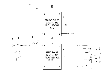
Figure 1 is a circuit diagram showing generally a
configuration of a discharge excitation type pulse laser
apparatus according to a first embodiment of the present
invention and Fig. 2 is a voltage waveform diagram for
illustrating operation of the discharge excitation type pulse
laser apparatus of the instant embodiment. Parenthetically,
Fig. 2 will also be referred to in describing a third
embodiment of the invention.
Referring to Fig. 1, the discharge excitation type
pulse laser apparatus according to the instant embodiment
includes a charging reactor 18, a first saturable reactor 19,
a first pulse generating four-terminal circuit 22 serving as
a first pulse generating circuit, and a second pulse
generating four-terminal circuit 23 serving as a second pulse
generating circuit in addition to the components of the
conventional discharge excitation type pulse laser apparatus
described hereinbefore by reference to Fig. 17.
The charging reactor 18 has one end connected to
the charging terminal 6 while the other end of the reactor 18
is connected to a junction at which the first and second
saturable reactors 19 and 21 are connected to each other.
The first saturable reactor 19 has one end
connected to the first terminal A of the first pulse
generating four-terminal circuit 22 and the other end
connected to one end of the switching device 8 which may be
constituted by a discharge type switch having a spark gap in
which electric discharge is caused to take place for
effecting the switching operation. The other end of the
switching device 8 is connected to a second terminal B of the
first pulse generating four-terminal circuit 22 as well as to
a second terminal B of the second pulse generating four-
terminal circuit 23.
On the other hand, one end of the second saturable
reactor 21 is connected to a first terminal A of the second
pulse generating four-terminal circuit 23 while the other end
of the second saturable reactor 21 is connected to the one
end of the switching device 8.
- 20 -
2161989
The first pulse generating four-terminal circuit 22
has a third terminal C and a fourth terminal D which are
connected to the first and second main discharge electrodes 2
and 3, respectively, while the third terminal C and the
fourth terminal D of the second pulse generating four-
terminal circuit 23 are connected to the second main
discharge electrode 3 and the auxiliary discharge electrode
4, respectively.
Next, operation of the discharge excitation type
pulse laser apparatus will be described by reference to a
waveform diagram of Fig. 2.
Assuming now that an electric discharge takes place
in the spark gap of the switching device 8 at a time
point t (= O), the directions of the currents flowing through
the first and second saturable reactors 19 and 21 are
reversed relative to those of the currents flowing through
these reactors upon charging thereof. Accordingly, the cores
of these reactors 18 and 21 assume the unsaturated states,
respectively. Thus, the first and second saturable reactors
19 and 21 can now operate as the reactors each of a large
capacity, as described hereinbefore in conjunction with the
conventional apparatus by reference to Fig. 18, as a result
of which operation of the first pulse generating four-
terminal circuit 22 as well as that of the second pulse
generating four-terminal circuit 23 is suppressed. In the
meanwhile, the spark gap of the switching device 8 assumes a
fully conducting state (i.e., fully closed state) with the
stray inductance and resistance components being suppressed
to a minimum. At a time point t (= Ts2), the core of the
second saturable reactor 21 is fully saturated, as a result
of which the inductance of the saturable reactor 21 steeply
decreases nonlinearly. At this time point (i.e., t (= Ts2)),
however, the inductance of the first saturable reactor 19
still remains at a large value. As a consequence, the
voltage outputted from the second pulse generating four-
terminal circuit 23 rises up at a high speed or rate because
the stray inductance and resistance components of the spark
- 21 -
2161q89
gap of the switching device 8 are suppressed to minimum
values, respectively, as mentioned above.
Referring continuously to Fig. 2, when the core of
the first saturable reactor 19 becomes the saturated at a
time point t (= Tsl) in the course of the discharge, the
inductance of the first saturable reactor 19 steeply
decreases nonlinearly. As can be seen from a waveform 1
shown in Fig. 2, the rise-up rate of the pulse-like voltage
applied across the first and second main discharge electrodes
2 and 3 is determined by the value of the inductance
decreased steeply. In other words, the pulse-like voltage
applied between the first and second main discharge
electrodes 2 and 3 rises up at a high rate, as in the case of
the conventional discharge excitation type pulse laser
apparatus shown in Fig. 17. Consequently, the discharge
start voltage (firing potential) VB becomes high, whereby the
energy injected into the main discharge 17 is increased.
Thus, the problem of the conventional discharge excitation
type pulse laser apparatus mentioned hereinbefore can
successfully be solved.
Embodiment 2
Next, a discharge excitation type pulse laser
apparatus according to a second embodiment of the invention
will be described by reference to a circuit diagram of
Fig. 3, in which like reference numerals as those used in
Figs. 1 and 17 denote like or equivalent parts. The
discharge excitation type pulse laser apparatus according to
the instant embodiment now under consideration differs from
the apparatus of the first embodiment in that a saturable
transformer 24 is employed in place of both the first and
second saturable reactors 19 and 21, wherein one end of a
primary winding of the saturable transformer 24 is connected
to the first terminal A of the first pulse generating four-
terminal circuit 22 with the other end thereof being
connected to one end of the charging reactor 18. On the
other hand, both ends of a secondary winding of the saturable
transformer 24 are connected to the first and second
- 22 -
2161989
terminals A and B of the second pulse generating four-
terminal circuit 23, respectively.
Now, operation of the discharge excitation type
pulse laser apparatus according to the instant embodiment of
the invention will be elucidated by reference to a waveform
diagram of Fig. 4.
It is assumed that electric discharge takes place
in the spark gap of the switching device 8 at a time point
t (= O). Then, a voltage is induced in the secondary winding
of the saturable transformer 24 to cause the second pulse
generating four-terminal circuit 23 to perform the charging
operation for the preionization. However, operation of the
first pulse generating four-terminal circuit 22 is inhibited
until the core of the saturable transformer 24 has attained
the magnetically saturated state. In the meanwhile, the
spark gap of the switching device 8 assumes a fully
conducting state (i.e., the switching device 8 is closed
fully or completely, to say in another way), which in turn
means that the stray inductance and resistance components of
the switching device 8 become minimum.
Further referring to Fig. 2, when the core of the
saturable transformer 24 assumes the magnetically saturated
state at a time point t (= Tsl) in the course of progress of
the discharge process, the inductance of the saturable
transformer 24 steeply decreases nonlinearly. As mentioned
hereinbefore, the rise-up rate of the pulse-like voltage
making appearance across the first and second main discharge
electrodes 2 and 3 is determined by the value of the
inductance of the transformer 24 decreased steeply. In other
words, the pulse-like voltage between the first and second
main disc~rarge electrodes 2 and 3 rises up at a high rate as
described hereinbefore by reference to Fig. 18 in conjunction
with the conventional discharge excitation type pulse laser
apparatus. Consequently, the discharge start voltage (firing
potential) VB becomes high, whereby the energy injected into
the main discharge 17 is caused to increase.
At this juncture, it should be mentioned that in
- 23 -
- ~161989
the discharge excitation type pulse laser apparatuses
according to the first and second embodiments of the
invention the first pulse generating four-terminal circuit 22
may be implemented in any appropriate circuit configuration
so far as it can apply a predetermined pulse-like discharging
voltage across the second main discharge electrode 3 and the
auxiliary discharge electrode 4. Similarly, the second pulse
generating four-terminal circuit 23 may be constituted by a
circuit of any suitable configuration so far as a
predetermined corona discharge trigger-pulse like voltage can
be applied across the auxiliary discharge electrode 4 and the
second main discharge electrode 3.
Embodiment 3
Figure 5 is a circuit diagram showing a third
embodiment of the invention which is directed to preferred
circuit configurations of the first and second pulse
generating four-terminal circuits 22 and 23, respectively,
which can be employed in the discharge excitation type pulse
laser apparatus shown in Fig. 1. In Fig. 5, parts same as or
equivalent to those shown in Fig. 1 and Fig. 17 are denoted
by like reference characters and repeated description thereof
is omitted.
More specifically, in the first pulse generating
four-terminal circuit 22 shown in Fig. 5, a first charging
capacitor 9 is connected to the first terminal A and the
third terminal C of the first pulse generating four-terminal
circuit 22, wherein a charging reactor 14a and the peaking
capacitor 13 are connected in parallel with each other and
inserted between a connecting conductor interconnecting the
first charging capacitor 9 and the third terminal C and a
connecting conductor interconnecting the second terminal B
and the fourth terminal D. The charging reactor 14a and the
peaking capacitor 13 cooperate to constitute a first charging
circuit means in the discharge excitation type pulse laser
apparatus according to the present invention.
On th~e other hand, in the second pulse generating
four-terminal circuit 23a, a second charging capacitor 12 is
- 24 -
2161989
connected between the first terminal A and the third terminal
C of the second pulse generating four-terminal circuit 23a,
wherein the second terminal B and the fourth terminal D are
connected to the ground potential. A charging reactor 15a is
connected between the second main discharge electrode 3 and
the auxiliary discharge electrode 4. Further, one end of a
second charging capacitor 12 is connected directly to the
third terminal C and at the same time to the fourth terminal
D of the first pulse generating four-terminal circuit 22
indirectly via the charging reactor 15a. To say in another
way, the second charging capacitor 12 is connected to the
ground potential via the third terminal C of the second pulse
generating four-terminal circuit 23a and the charging reactor
15a as well as the fourth terminal D and the second terminal
B of the first pulse generating four-terminal circuit 22.
The charging reactor 15a constitutes the second charging
circuitry means of the discharge excitation type pulse laser
apparatus according to the invention.
Next, referring to Fig. 2, description will turn to
operation of the discharge excitation type pulse laser
apparatus according to the instant embodiment. As mentioned
previously in conjunction with the conventional pulse laser
apparatus, the first and second charging capacitors 9 and 12
are first charged via the charging reactor 18. Through this
charging process, the cores of the first and second saturable
reactors 19 and 21 are set to the state saturated with one
polarity. When the spark gap of the switching device 8 is
fired at a time point t (= O), the first and second charging
capacitors 9 and 12 start to discharge. At this time, the
directions of the currents flowing through the first and
second saturable reactors 19 and 21 are reversed relative to
the directions of the currents flowing through these reactors
upon charging thereof. Consequently, the cores of the first
and second saturable reactors 19 and 21 become unsaturated.
Thus, the first and second saturable reactors 19 and 21
function as the reactors each exhibiting a large capacity to
thereby suppress the discharges of the first and second
- 25 -
2l6l989
charging capacitors 9 and 12, as described hereinbefore by
reference to the waveform diagram of Fig. 18, In the
meanwhile, the spark gap of the switching device 8 becomes
fully conducting (i.e., the switching device 8 is closed
completely in the equivalent sense) with the stray inductance
and resistance components decreasing to minimum.
At a time point t (= Ts2), the core of the second
saturable reactor 21 becomes magnetically saturated with the
inductance thereof steeply decreasing nonlinearly. At this
time point, however, inductance of the first saturable
reactor 19 continues to be of a large value. The stray
inductance and resistance components of the switching device
8 is minimized. Thus, the second charging capacitor 12 can
discharge at a high rate, as a result of which the
preionization of the space between the main electrodes 2 and
3 due to the corona discharge 16 is accelerated remarkably.
In this manner, the effect aimed by the invention can be
achieved owing to the increasing of the capacity of the first
saturable reactor 19.
Now, when a time point t (= Tsl) is reached as the
discharge process progresses, the core of the first saturable
reactor 19 becomes magnetically saturated, as a result of
which inductance thereof steeply decreases nonlinearly, as
can be seen in Fig. 2. The rise-up rate of the pulse-like
voltage applied across the first and second main discharge
electrodes 2 and 3 is determined by the steeply decreased
value of the inductance mentioned above, as can be seen from
the waveform 1 shown in Fig. 2. In this way, the pulse-like
voltage between both the first and second main discharge
electrodes 2 and 3 rises up at a high rate with the discharge
start voltage (firing potential) VB being increased, which of
course contribute to increasing of the amount of energy
injected into the main discharge 17. Thus, it can be
appreciated that the problem of the hitherto known laser
apparatus pointed out hereinbefore can successfully be solved
by the instant embodiment of the invention.
Embodiment 4
- 26 -
2161~89
Next, a fourth embodiment of the present invention
will be described by reference to a circuit diagram of
Fig. 6.
The instant embodiment now under consideration
differs from the third embodiment described above in respect
to the configuration of the second pulse generating four-
terminal circuit 23 which is generally denoted by a reference
character-~3b in Fig. 6. In the case of the second pulse
generating four-terminal circuit 23b of the discharge
excitation type pulse laser apparatus according to the
instant embodiment, one end of the second charging capacitor
12 is connected to the second saturable reactor 21 via the
first terminal A while the other end of the second charging
capacitor 12 is connected to one end of a third saturable
reactor 25 which has the other end connected to the auxiliary
discharge electrode 4 via the third terminal C. Furthermore,
a parallel connection of a charging reactor 26 and a first
charge transfer capacitor 27 is inserted between a junction
at which the second charging capacitor 12 and the third
saturable reactor 25 are interconnected and the second and
fourth terminals B and D which are connected to the ground
potential.
-Now, referring to a waveform diagram of Fig. 7,
description will turn to operation of the discharge
excitation type pulse laser apparatus according to the
instant embodiment of the invention. As mentioned previously
in conjunction with the conventional pulse laser apparatus,
the first and second charging capacitors 9 and 12 are first
charged via the charging reactor 18. In the course of this
charging process, the cores of the first and second saturable
reactors 19 and 21 are set to the state saturated with one
polarity. When the spark gap of the switching device 8 is
fired (i.e., when the switching device 8 becomes conductive)
at a time point t (= O), each of the first and second
charging capacitors 9 and 12 starts to discharge. At this
time, the directions of the currents flowing through the
first and second saturable reactors 19 and 21 are reversed
2161989
relative to the directions upon charging of these reactors.
Consequently, the cores of the first and second saturable
reactors 19 and 21 become unsaturated. Thus, each of the
first and second saturable reactors 19 and 21 exhibits a
large capacity and functions as to suppress the discharges of
the first and second charging capacitors 9 and 12. In the
meanwhile, the spark gap of the switching device 8 becomes
fully conducting with the stray inductance and resistance
components being suppressed to a minimum.
Now, at a time point t (= Ts2) at which the core of
the second saturable reactor 21 assumes the saturated state,
the inductance thereof steeply decreases nonlinearly. At
this time point, however, the inductance of the first
saturable reactor 19 continues to be of a large value with
the stray inductance and resistance components of the
switching device 8 being minimized. As a consequence, charge
transfer to the first charge transfer capacitor 27 from the
second charging capacitor 12 is accelerated.
Subsequently, at a time point t (= Ts3), the core
of the third saturable reactor 25 becomes magnetically
saturated with the inductance thereof steeply decreasing
nonlinearly. Because the loop extending from the first
charge transfer capacitor 27 to the auxiliary discharge
electrode 4 by way of the third saturable reactor 25 which is
saturated exhibits inductance smaller than that of the loop
formed by the spark gap of the switching device 8, the second
saturable reactor 21, the second charging capacitor 12 and
the first charge transfer capacitor 27, the voltage applied
to the auxiliary discharge electrode 4 rises up more steeply,
to thereby promote more intensively the preionization by the
corona discharge 16.
Now, when a time point t (= Tsl) is reached as the
discharge process progresses, the core of the first saturable
reactor 19 becomes magnetically saturated, as a result of
which inductance thereof steeply decreases nonlinearly, as
can be seen in Fig. 7. Consequently, the rise-up rate of the
pulse-like voltage applied across the first and second main
- 28 -
2161989
discharge electrodes 2 and 3 is determined by the value of
the steeply lowered inductance. Thus, as can be seen from
the waveform 1 shown in Fig. 7, the pulse-like voltage
between borth the first and second main discharge electrodes 2
and 3 rises up at a high rate with the discharge start
voltage (firing potential) VB being increased, which of
course contribute to increasing of the amount of energy
injected into the main discharge path 17. It is apparent
that the problem of the conventional discharge excitation
type pulse laser apparatus mentioned hereinbefore can equally
be solved by the instant embodiment of the invention.
Embodiment 5
Next, a fifth embodiment of the present invention
will be described by reference to a circuit diagram of
Fig. 8.
The discharge excitation type pulse laser apparatus
now under consideration differs from the fourth embodiment
described above in respect to the configuration of the second
pulse generating four-terminal circuit which is generally
denoted by a reference character 23c in Fig. 8. More
specifically, the charging reactor 26 and the first charge
transfer capacitor 27 connected in parallel and having one
ends connected to the junction between the second charging
capacitor 12 and the third saturable reactor 25 have the
respective other ends connected mutually and connected to the
ground potential by way of the second terminal B (i.e.,
connected to the second main discharge electrode 3), wherein
the other end of the third saturable reactor 25 is connected
to the one end of a fourth saturable reactor 28 which has the
other end connected to the auxiliary discharge electrode 4
via the third terminal C. The junction between the third
saturable reactor 25 and the fourth saturable reactor 28 is
connected to the ground potential by way of the second charge
transfer capacitor 29 and the fourth terminal D thereof
(i.e., the junction mentioned above is connected to the
second main discharge electrode 3, to say in another way).
Further, the grounded ends of the first and second charge
- 29 -
2161989
transfer capacitors 27 and 29 are connected to each other.
Next, description will turn to operation of the
discharge excitation type pulse laser apparatus according to
the instant embodiment. As mentioned previously in
conjunction with the conventional pulse laser apparatus, the
first and second charging capacitors 9 and 12 are first
charged via the charging reactor 18. Through this charging
process, the cores of the first and second saturable reactors
19 and 21 are set to the state saturated with one polarity.
When the spark gap of the switching device 8 is fired at the
time point t (= O), each of the first and second charging
capacitors 9 and 12 starts to discharge. At this time point,
the currents flowing through the first and second saturable
reactors 19 and 21 are reversed in respect to the directions
of the currents flowing through these reactors upon charging
thereof. Consequently, the cores of the first and second
saturable reactors 19 and 21 become unsaturated. Thus, the
first and second saturable reactors 19 and 21 function as the
reactors each exhibiting a large capacity to thereby suppress
the discharge of the first and second charging capacitors 9
and 12. In the meanwhile, the spark gap of the switching
device 8 becomes fully conducting with the stray inductance
and resistance components decreasing to minimum.
At a time point t (= Ts2), the core of the second
saturable reactor 21 becomes magnetically saturated, upon
which the inductance thereof steeply decreases nonlinearly.
At this time point, however, the inductance of the first
saturable reactor 19 continues to be of a large value while
the stray inductance and resistance component of the
switching device 8 become minimum. Thus, the charge transfer
from the second charging capacitor 12 to the first charge
transfer capacitor 27 is started at a high rate.
Subsequently, at a time point t (= Ts3), the core
of the third saturable reactor 25 becomes magnetically
saturated with the inductance thereof steeply decreasing
nonlinearly. Because the loop for transferring the electric
charge from the first charge transfer capacitor 27 to the
- 30 -
2 1 6 1 989
second charge transfer capacitor 29 by way of the third
saturable reactor 25 which is in the saturated state has an
inductance smaller than that of the loop formed by the spark
gap of the switching device 8, the second saturable reactor
21, the second charging capacitor 12 and the first charge
transfer capacitor 27, the voltage applied to the second
charge transfer capacitor 29 can rise up more steeply, to
thereby promote the preionization by the corona discharge 16.
By the way, it should be mentioned that when an
electron adhesive gas such as a gas mixture of F2 and Cl2 or
the like is hermetically filled in the laser chamber 1, the
quantity of electrons once generated by the preionization
tends to decrease due to absorption by these electron
adhesive gases. However, this problem can satisfactorily be
solved by-the structure of the discharge excitation type
pulse laser apparatus according to the instant embodiment of
the invention.
Figure 9 shows the waveforms of the individual
pulse-like voltages for illustrating operation of the pulse
laser apparatus described above. In the discharge excitation
type pulse laser apparatus according to the instant
embodiment of the invention, such arrangement is adopted that
the inductance of the fourth saturable reactor 28 can
continuously remain at a large value until the voltage
applied to the second charge transfer capacitor 29 rises up.
As the discharge process progresses as shown in
Fig. 9, the core of the first saturable reactor 19 becomes
magnetically saturated at a time point t (= Tsl), being
accompanied with nonlinear steep decrease of the first
saturable-reactor 19. At the same time, the core of the
fourth saturable reactor 28 is changed over to the
magnetically saturated state with the inductance thereof
steeply lowering nonlinearly, which results in that the
voltage applied across the auxiliary discharge electrode 4
and the second main discharge electrode 3 increases steeply.
As a consequence, the timing at which the first main
discharge electrode 2 rises up coincides with the timing at
- 31 -
2 t 6 1 989
..
which the voltage applied across the auxiliary discharge
electrode 4 and the second main discharge electrode 3 rises
up steeply. As a consequence, the timing at which the first
main discharge electrode 2 rises up coincides with the timing
at which the voltage of the waveform 1 makes appearance
between the first and second main discharge electrodes 2 and
3. Thus, the unwanted phenomenon that electrons generated
upon the preionization by the corona discharge are absorbed
by the laser gas can satisfactorily be suppressed, which
allows smooth transition to the main discharge.
In the case of the second pulse generating four-
terminal circuit 23c described above, one fourth saturable
reactor 28 and one second charge transfer capacitor 29 are
additionally inserted, respectively, between the third
saturable reactor 25 and the auxiliary discharge electrode 4.
It goes however without saying that a plurality of additional
saturable reactors may be connected in series with a
corresponding number of charge transfer capacitors connected
to each of the saturable reactors, respectively.
Embodiment 6
A sixth embodiment of the invention is directed to
concrete circuit configurations of the first pulse generating
four-terminal circuit 22 and the second pulse generating
four-terminal circuit 23, respectively, which will be
described below by reference to Fig. 10.
As can be seen in Fig. 10, one end of the secondary
winding of the saturable transformer 24 is connected directly
to the second terminal B of the first pulse generating four-
terminal circuit 22 and indirectly to the second main
discharge electrode 3 by way of the fourth terminal D. On
the other hand, the other end of the secondary winding of the
saturable transformer 24 is connected to the first terminal A
of the second pulse generating four-terminal circuit which is
denoted by 23h, wherein the first terminal A and the second
terminal B of the second pulse generating four-terminal
circuit 23h are directly connected to each other by a
connecting conductor. Further, the third terminal C of the
- 32 -
2161~89
second pulse generating four-terminal circuit 23h is
connected to the auxiliary discharge electrode 4. The second
terminal B and the fourth terminal D of the second pulse
generating four-terminal circuit 23h are directly
interconnected and at the same time connected to the ground
potential.
Next, operation of the discharge excitation type
pulse laser apparatus according to the instant embodiment of
the invention will be described by reference to Fig. 4. At
first, the first charging capacitor 9 is charged by way of
the charging reactor 14a. During this charging process, the
core of the saturable transformer 24 is magnetically
saturated with one polarity. When the spark gap of the
switching device 8 is fired at a time point t (= O), the
first charging capacitor 9 starts to discharge. Since the
direction of the current flowing through the saturable
transformer 24 at this time point is reversed relative to
that of the current flowing therethrough during the charging
process, the core of the saturable transformer 24 is changed
over to the unsaturated state. Thus, when the spark gap of
the switching device 8 is closed, a voltage having a steep
rise-up edge is induced in the secondary winding of the
saturable transformer 24. At this time point, the inductance
of the saturable transformer 24 is, however, of a large
value. As a consequence, the discharge of the first charging
capacitor 9 is suppressed. In the meanwhile, the spark gap
of the switching device 8 becomes fully closed (i.e., fully
conducting). Thus, the stray inductance and resistance
components of the switching device 8 become minimum.
Now, when a time point t (= Tsl) is reached as the
discharge process progresses, the core of the saturable
transformer 24 becomes magnetically saturated as a result of
which inductance thereof steeply decreases nonlinearly, as
can be seen in Fig. 4. The rise-up rate of the pulse-like
voltage applied across the first and second main discharge
electrodes 2 and 3 is determined by the steeply lowered value
of the above-mentioned inductance, as can be seen from the
- 33 -
2161989
waveform 1 illustrated in Fig. 4. In this manner, the pulse-
like voltage applied between both the first and second main
discharge electrodes 2 and 3 rises up at a high rate with the
discharge start voltage (firing potential) V3 increasing,
which of course contribute to increasing of the energy
injected into the main discharge 17.
Embodiment 7
Figure 11 is a circuit diagram showing a structure
of the discharge excitation type pulse laser apparatus
according to a seventh embodiment of the present invention.
The discharge excitation type pulse laser apparatus
now under consideration differs from the second embodiment in
that the first terminal A connected to the saturable
transformer 24 of the first pulse generating four-terminal
circuit 22a and the third terminal C connected to the first
main discharge electrode 2 are directly connected to each
other, while the second terminal B of the first pulse
generating four-terminal circuit 22a and the fourth terminal
D thereof are mutually connected, wherein a peaking capacitor
13 is inserted between the junction of the first terminal A
and the third terminal C and the junction of the second
terminal B and the fourth terminal D.
Further, one end of a primary winding of the
saturable transformer 24 is connected to the first terminal A
of the first pulse generating four-terminal circuit 22a,
while the other end of the primary winding is connected to
one terminal of a switching pulse generating circuit 31 which
serves as a pulse generating means and has the other terminal
to which the second terminal B of the first pulse generating
four-terminal circuit 22a is connected. Connected between
both terminals of the switching pulse generating circuit 31
is the first charging capacitor 9.
The saturable transformer 24 has a secondary
winding having one end connected to the first terminal A of
the second pulse generating four-terminal circuit 23d and the
other end connected to the second terminal B thereof, wherein
the second charging capacitor 12 is connected between the
- 34 -
2161989
first and second terminals A and B with the second terminal B
being connected to the fourth terminal D which is grounded.
Additionally, the second saturable reactor 21 is inserted
between the first terminal A and the third terminal C of the
second pulse generating four-terminal circuit 23d.
Now, description will turn to operation of the
discharge excitation type pulse laser apparatus according to
the instant embodiment by reference to Fig. 9. At first, a
pulse-like voltage is generated by the switching pulse
generating circuit 31 at a time point t (= O), whereby the
first charging capacitor 9 is charged. At this time point,
the core of the saturable transformer 24 is not yet
saturated, and a voltage is induced in the secondary winding
thereof upon charging of the first charging capacitor 9.
Since the saturable transformer 24 exhibits a large
inductance, the charging of the peaking capacitor 13 is
suppressed. On the other hand, the second charging capacitor
12 is charged by the voltage induced in the secondary winding
of the saturable transformer 24. At this time point,
however, the second saturable reactor 21 is in the
unsaturated state. Consequently, the voltage of the second
charging capacitor 12 is prevented from being applied to the
auxiliary discharge electrode 4.
Now, when a time point t (= Tsl) is reached as the
discharge process progresses, the core of the first saturable
reactor 19 becomes magnetically saturated, as a result of
which inductance thereof steeply decreases nonlinearly, as
can be seen in Fig. 9. The rise-up rate of the pulse-like
voltage applied across the first and second main discharge
electrodes 2 and 3 is determined by the steeply lowered value
of the above-mentioned inductance, as can be seen from the
waveform 1 shown in Fig. 9. In this manner, the pulse-like
voltage applied between both the first and second main
discharge electrodes 2 and 3 rises up at a high rate because
of the low inductance of the circuit with the discharge start
voltage (firing potential) V3 being increased, which of
course contributes to increasing of the energy injected into
- 35 -
2161989
the main discharge 17. Since the second saturable reactor 21
is so arranged as to be saturated with the inductance thereof
lowering steeply, the voltage applied across the auxiliary
discharge electrode 4 and the second main discharge electrode
3 rises up steeply simultaneously with the rise-up of the
voltage applied across the first and second main discharge
electrodes 2 and 3, as can be seen from the waveform 2 shown
in Fig. 9. As a result of this, the corona discharge takes
place to preionize the space existing between the first and
second main discharge electrodes 2 and 3.
Embodiment 8
Figure 12 is a circuit diagram showing a structure
of the discharge excitation type pulse laser apparatus
according to an eighth embodiment of the present invention.
The discharge excitation type pulse laser apparatus
now of concern is implemented similarly to the apparatus
shown in Fig. 5 (third embodiment) except for the structure
of the second pulse generating four-terminal circuit. More
specifically, there is inserted between the first terminal A
and the third terminal C of the second pulse generating four-
terminal circuit denoted by 23e a series connection of the
second charging capacitor 12 and a coaxial cable 20 which
serves as a delay circuit. Both ends of the coaxial cable 20
are connected to the ground potential via the second and
fourth terminals B and D, respectively.
Next, description will turn to operation of the
discharge excitation type pulse laser apparatus according to
the instan-t embodiment by reference to Fig. 13. As mentioned
previously in conjunction with the conventional pulse laser
apparatus, the first and second charging capacitors 9 and 12
are first charged via the charging reactor 18. Through this
charging process, the cores of the first and second saturable
reactors 19 and 21 are set to the state saturated with one
polarity. When the spark gap of the switching device 8 is
fired at a time point t (= 0), each of the first and second
charging capacitors 9 and 12 starts to discharge. At this
time point, the direction of the currents flowing through the
- 36 -
21~1989
first and second saturable reactors 19 and 21 is reversed
relative to the direction of the currents flowing upon
charging. Consequently, the cores of the first and second
saturable reactors 19 and 21 become unsaturated. Thus, the
first and second saturable reactors 19 and 21 function as the
reactors each exhibiting a large capacity to thereby prevent
the first and second charging capacitors 9 and 12 from
discharging. In the meanwhile, the spark gap of the
switching device 8 becomes fully conducting (i.e., the
switching device 8 is closed completely in the equivalent
sense) with the stray inductance and resistance components
decreasing to a minimum.
At a time point t (= Ts2), the core of the second
saturable reactor 21 becomes magnetically saturated, upon
which inductance thereof steeply decreases nonlinearly. At
this time point, however, inductance of the first saturable
reactor 19 continues to be of a large value with the stray
inductance and resistance components of the switching device
8 being minimized. For this reason, the second charging
capacitor 12 discharges at a high rate, as a result of which
the preionization by the corona discharge 16 is promoted
remarkably. However, because of the presence of the coaxial
cable 20 which functions as the delay circuit, the voltage
making appearance between the auxiliary discharge electrode 4
and the second main discharge electrode 3 can not yet reach
the level required for allowing the discharge to occur
between these electrodes.
Now, when a time point t (= Tsl) is reached as the
discharge process progresses, the core of the first saturable
reactor 19 becomes magnetically saturated as a result of
which inductance thereof steeply decreases nonlinearly, as
can be seen in Fig. 13. The rise-up rate of the pulse-like
voltage applied across the first and second main discharge
electrodes 2 and 3 is determined by the steeply decreased
value of the above-mentioned inductance, as can be seen from
the waveform 1 shown in Fig. 13. In this way, the pulse-like
voltage between both the first and second main discharge
- 37 -
216198~
electrodes 2 and 3 rises up at a high rate with the discharge
start voltage (firing potential) V3 being increased, which of
course contributes to increasing of the energy injected into
the main discharge path 17.
Further, at this time point, the voltage 12 making
appearance across the second charging capacitor 12 with a
time delay involved by the coaxial cable 20 is applied to the
auxiliary discharge electrode 4, as a result of which the
voltage between the auxiliary discharge electrode 4 and the
second main discharge electrode 3 rises up steeply. Thus,
the timing at which the pulse-like voltage of the waveform 2
rises up coincides with that of the pulse-like voltage of the
waveform 1 between the first and second main discharge
electrodes 2 and 3, whereby the unwanted phenomenon that
electrons generated by the preionization under the effect of
the corona discharge are absorbed by the laser gas can
essentially be prevented. Thus, the transition to the
primary or main discharge from the corona discharge
(auxiliary discharge) can smoothly be realized.
Embodiment 9
Figure 14 is a circuit diagram showing a structure
of the discharge excitation type pulse laser apparatus
according to a ninth embodiment of-the present invention
which differs from the apparatus shown in Fig. 12 in respect
to the structure of the second pulse generating four-terminal
circuit which is denoted by 23f in Fig. 14. More
particularly, referring to Fig. 14, connected between the
first terminal A and the third terminal C of the second pulse
generating four-terminal circuit 23f are a second charging
capacitor 12, a third saturable reactor 25 and a coaxial
cable 20 serving as a delay circuit which are serially
connected in this order, wherein a charging reactor 26 and a
first charge transfer capacitor 27 are connected in parallel
with each other between the second terminal B and wiring
conductor interconnecting the second charging capacitor 12
and the third saturable reactor 25, while the charging
reactor 15a is inserted between the second terminal B and a
- 38 -
2161989
connecting conductor which interconnects the third saturable
reactor 25 and the coaxial cable 20. In this conjunction, it
should however be mentioned that the charging reactor 15a may
be connected between the second main discharge electrode 3
and the auxiliary discharge electrode 4 instead of connecting
the charging reactor 15a in the manner mentioned above.
Next, description will turn to operation of the
discharge excitation type pulse laser apparatus according to
the instant embodiment by reference to the waveform diagram
of Fig. 13. As mentioned previously in conjunction with the
conventional pulse laser apparatus, the first and second
charging capacitors 9 and 12 are first charged via the
charging reactor 18. Through this charging process, the
cores of the first and second saturable reactors 19 and 21
are set to the state saturated with one polarity. When the
spark gap of the switching device 8 is fired at a time point
t (= 0), each of the first and second charging capacitors 9
and 12 starts to discharge. At that time, the currents
flowing through the first and second saturable reactors 19
and 21 are reversed relative to the directions of the
currents flowing through these reactors upon charging
thereof. Consequently, the cores of the first and second
saturable reactors 19 and 21 become unsaturated. Thus, the
first and second saturable reactors 19 and 21 function as the
reactors each exhibiting a large capacity to suppress the
discharges of the first and second charging capacitors 9 and
12. In the meanwhile, the spark gap of the switching device
8 becomes fully conducting (i.e., the switching device 8 is
closed completely in the equivalent sense) with the stray
inductance and resistance components decreasing to minimum.
At a time point t (= Ts2), the core of the second
saturable reactor 21 assumes the magnetically saturated
state, and thus the inductance thereof steeply decreases
nonlinearly. At this time point, however, inductance of the
first saturable reactor 19 continues to be of a large value
with the stray inductance and resistance components of the
switching device 8 being minimized. For this reason, charge
- 39 -
2161989
transfer to the first charge transfer capacitor 27 from the
second charging capacitor 12 is promoted.
Subsequently, at a time point t (= Ts3), the core
of the third saturable reactor 25 becomes magnetically
saturated with the inductance thereof thus abruptly
decreasing nonlinearly. Because the loop for transferring
the electric charge to the coaxial cable 20 by way of the
third saturable reactor 25 which is now saturated has the
inductance smaller than that of the loop formed by the spark
gap of the switching device 8, the second saturable reactor
21, the second charging capacitor 12 and the first charge
transfer capacitor 27, the voltage applied to the coaxial
cable 20 rises up more steeply to thereby accelerate the
preionization by the corona discharge 16. However, because
of the presence of the coaxial cable 20 functioning as the
delay circuit, the voltage making appearance between the
auxiliary discharge electrode 4 and the second main discharge
electrode 3 can not immediately increase to a sufficiently
high level for the corona discharge to take place.
Now, when a time point t (= Tsl) is reached as the
discharge process progresses, the core of the first saturable
reactor 19 becomes magnetically saturated, as a result of
which the inductance thereof steeply decreases nonlinearly,
as can be seen in Fig. 13. The rise-up rate of the pulse-
like voltage applied across the first and second main
discharge electrodes 2 and 3 is determined by the value of
the steeply decreased inductance value, as can be seen from
the waveform 1 shown in Fig. 13. In this manner, the pulse-
like voltage between both the first and second main discharge
electrodes 2 and 3 rises up at a high rate with the discharge
start voltage (firing potential) V3 being increased, which of
course contributes to increasing the amount of energy
injected into the main discharge 17. Further, at this time
point, the voltage 12 making appearance across the second
charging capacitor 12 with a time delay involved by the
coaxial cable 20 is applied to the auxiliary discharge
electrode 4, as a result of which the voltage between the
- 40 -
216198~
auxiliary discharge electrode 4 and the second main discharge
electrode 3 rises up steeply. Thus, the timing at which the
pulse-like voltage of the waveform 2 rises up coincides with
that of the pulse-like voltage of the waveform 1 between the
first and second main discharge electrodes 2 and 3, whereby
the unwanted phenomenon that electrons generated by the
preionization due to the corona discharge are absorbed by the
laser gas can essentially be prevented. Thus, transition to
the primary or discharge from the corona discharge (auxiliary
discharge) can smoothly be realized.
Embodiment-10
Figure 15 is a circuit diagram showing a structure
of the discharge excitation type pulse laser apparatus
according to a tenth embodiment of the present invention.
The discharge excitation type pulse laser apparatus
now of concern is implemented similarly to the apparatus
shown in Fig. 10 (third embodiment) except for the structure
of the second pulse generating four-terminal circuit which is
denoted by 23g in Fig. 15. Referring to this figure, there
is inserted between the first terminal A and the third
terminal C of the second pulse generating four-terminal
circuit 23g a coaxial cable 20 which serves as a delay
circuit. Both ends of the coaxial cable 20 are connected to
the second and fourth terminals B and D, respectively, both
of which are is connected to the ground potential. Further,
both ends of the secondary winding of the saturable
transformer 24 are connected to the first terminal A and the
second terminal B, respectively, of the second pulse
generating four-terminal circuit 23g.
Next, operation of the discharge excitation type
pulse laser apparatus according to the instant embodiment of
the invention will be described by reference to Fig. 13. At
first, the first charging capacitor 9 is charged by way of
the charging reactor 18. Due to this charging process, the
core of the saturable transformer 24 is set to the state
magnetically saturated with one polarity. When the spark gap
of the switching device 8 is fired at a time point t (= 0),
- 41 -
216~989
the first charging capacitor 9 starts to discharge. Since
the direction of the current flowing through the saturable
transformer 24 at this time point is reversed relative to the
current flowing therethrough during the charging process, the
core of the saturable transformer 24 is changed over to the
unsaturated state. Thus, when the spark gap of the switching
device 8 is closed, a voltage having a steep rise-up edge is
induced in the secondary winding of the saturable transformer
24. However, because of the presence of the coaxial cable 20
functioning as the delay circuit, the voltage making
appearance between the auxiliary discharge electrode 4 and
the second main discharge electrode 3 can not increase
sufficiently. Consequently, the corona discharge can not be
generated. At this time point, inductance of the saturable
transformer 24 is of a large value. As a consequence, the
discharge of the first charging capacitor 9 is suppressed.
In the meanwhile, the spark gap of the switching device 8
becomes fully closed (i.e., fully conducting). Thus, the
stray inductance and resistance components of the switching
device 8 become minimum.
Now, when the time point t (= Tsl) is reached as
the discharge process progresses, the core of the saturable
transformer 24 becomes magnetically saturated as a result of
which inductance thereof steeply decreases nonlinearly, as
can be seen in Fig. 13. The rise-up rate of the pulse-like
voltage applied across the first and second main discharge
electrodes 2 and 3 is determined by the steeply decreased
inductance value, as can be seen from the waveform 1 shown in
Fig. 4. In this way, the pulse-like voltage between both the
first and second main discharge electrodes 2 and 3 rises up
at a high rate with the discharge start voltage (firing
potential) VB increasing, which of course contribute to
increasing the energy injected into the main discharge path
17, as in the case of the conventional apparatus (see
Fig. 19). Further, at this time point, the voltage 12
induced across the secondary winding of the saturable
transformer 24 is applied to the auxiliary discharge
- 42 -
2161989
electrode 4 with a time delay involved by the coaxial cable
20, as a result of which the voltage between the auxiliary
discharge electrode 4 and the second main discharge electrode
3 rises up steeply. Thus, the timing at which the pulse-like
voltage of the waveform 2 rises up coincides with that of the
pulse-like voltage of the waveform 1 making appearance
between the first and second main discharge electrodes 2 and
3, whereby the unwanted phenomenon that electrons generated
by the preionization due to the corona discharge are absorbed
by the laser gas can essentially be prevented. Thus,
transition to the primary or main discharge from the corona
discharge (auxiliary discharge) can smoothly be realized.
Modifications
Many features and advantages of the present
invention are apparent form the detailed description and thus
it is intended by the appended claims to cover all such
features and advantages of the system which fall within the
true spirit and scope of the invention. Further, since
numerous modifications and combinations will readily occur to
those skilled in the art, it is not intended to limit the
invention to the exact structures and operations illustrated
and described.
By way of example, although it has been described
that the coaxial line (i.e., coaxial cable 20) is employed as
the pulse delay circuit, it should be understood that other
pulse delay circuits such as a strip line, an LC circuitry or
the like may be employed to the substantially same effects.
Besides, in place of employing the spark gap switch as the
switching element 8, other switching elements or circuitries
such as a thyratron, semiconductor switches (e.g. thyristor,
SIT transistor, FET (Field-Effect Transistor), IGBT
(Insulated Gate Bipolar Transistor), etc.), serial or
parallel connections thereof or a rail gap switch may be
employed without departing from the spirit and scope of the
invention. Furthermore, in the foregoing description of the
various embodiments of the invention, it has been assumed
that the charging is effected with positive (plus) polarity
- 43 -
2 1 6 1 989
from the charging terminal 6, it goes without saying that the
charging may be performed with negative (minus) polarity.
Additionally, the charging reactors 14, 15a and 26 employed
as the charging circuit components may be replaced by other
component such as resistors, diodes or the like substantially
to the same aimed effects. Besides, although the invention
has been described as being applied to the excimer laser, it
should be understood that the teachings of the invention can
equally be applied to other discharge excitation type lasers.
Moreover, it should be mentioned in connection with the
circuits shown in Fig. 5, 6, 8, 10, 12, 14 and 15 that the
first charging capacitor 9 and the first saturable reactor 19
or the saturable transformer 24 may be replaced with each
other in respect to the positions thereof, and the same holds
true for the positional relation between the second charging
capacitor 12 and the second saturable reactor 21.
Finally, it should be added that the electrodes
mentioned previously in conjunction with the various
embodiments of the invention may be implemented in such
structure as shown in Fig. 16. More specifically, the
second main discharge electrode 3a may be realized in a same
configuration as the first main discharge electrode 2,
wherein the auxiliary discharge electrode denoted by 4a in
Fig. 16 may be disposed at both or one side of the second
main discharge electrode 3a in such a state that the
auxiliary discharge electrode 4a is peripherally enclosed
with an insulation member 5a. In the case of such electrode
array, the corona discharge 16 is caused to take place
between the auxiliary discharge electrode 4a and the second
main discharge electrode 3a to thereby ionize previously the
space existing between the first and second main discharge
electrodes 2 and 3a so that the corona discharge can smoothly
transit to the main discharge 17.
Accordingly, all suitable modifications and
equivalents may be resorted to, falling within the spirit and
scope of the invention.
- 44 -