Note: Descriptions are shown in the official language in which they were submitted.
\...'
PATENT
450100-3367
BACKGROUND OF THE INVENTION
Field of the Invention.
The present invention relates to a
recording/reproducing apparatus and method for digitally
recording and reproducing a television signal.
Description of the Related Art
PAL plus and EDTV-2
Television signals are encoded using accepted encoding
standards. The United States adopted the NTSC (National
Television System Committee) standard of encoding television
signals, while Europe adopted the PAL (Phase Alternating Line)
standard. The NTSC and the PAL standards provide television
pictures with an aspect ratio of 4 . 3 (width . height), which is
considered poor because people normally view scenes with a wider
aspect.
In recent years, the PAL plus standard and the EDTV-2
(Enhanced Definition Television) standard have been proposed,
which have a high image quality, a wide screen feature, and a
compatibility with the PAL and the NTSC standards, respectively.
The aspect ratios of these wide screen standards are 16 . 9 and
14 . 9, which are considerably better than the 4 . 3 (12 . 9)
SONY(ecs)\3367.APP _
PATENT
450100-3367
standard. Thus, the PAL plus and EDTV-2 standards provide
viewers with superior image quality and a more realistic aspect
ratio.
In both the EDTV-2 and the PAL plus standards, the
higher aspect ratios are obtained by processing each screen
through a 4-to-3 line decimator. Each resulting screen may be
thought of as being in the shape of a letter box, as shown in
Fig. 1, bordered by invalid screen portions. For example, a
video signal is placed on the 360 lines at the main screen
portion of the display, but not on the upper and lower 60 lines.
In this manner, a flat screen with an aspect ratio of 16 . 9 is
obtained:
In the case of the PAL plus standard, the image quality
is preserved by generating a vertical resolution component known
as the helper signal. As shown in Fig. 2, the helper signal for
compensating the vertical resolution is multiplexed at the top
and bottom, invalid portions of the letter box shape screen. In
addition, a WSS signal, which signals the presence of the helper
signal and which includes the aspect ratio information, is stored
at invalid line 23. Reference signals, which are used'.to
reconstruct the helper signal, are also stored in the invalid
portions. A reference burst signal with a sub-carrier frequency
(4.43 MHz) is disposed at the second half of the line 23.
SONY(ecs)\3367.APP
PATENT
450100-3367
Moreover, a reference signal that represents the 100 % white
level is disposed on a line 623.
_ While the decimated screen is conveniently thought of as a
letter box, each line actually comprises an analog signal. As
shown in Fig. 3, line 23 is depicted as an analog signal
including a blanking signal, a color burst, the WSS signal, a
reference burst and another blanking signal. Fig. 4 depicts all
of the lines as analog signals and distinguishes between the
valid and vertical blanking intervals of the screen. It should
be noted that line 23, which is located in the upper invalid
portion, is considered valid according to Fig. 4 in the sense
that line 23 is not in the vertical blanking interval. Line 623
is in the vertical blanking interval because line 623 carries the
100% white level, which should not be displayed.
In the case of the EDTV-2 standard, as shown in Fig. 5,
VT and VH signals are multiplexed at the top and bottom of the
letter box screen, and an HH signal is multiplexed at the main
screen portion. The VT signal is a vertical time high band
component that is lost in the interlace process when a video
signal photographed in the double speed non-interlace mode is
transmitted by the interlace mode. The VH signal is a vertical
luminance high band component that is lost when a video signal
with an aspect ratio of 16 . 9 is formed by decimation into the
letter box shape. The HH signal is a horizontal luminance high
SONY(eca)\3367.APP _ 3 _
PATENT
450100-3367
band component with a band ranging from 4.2 MHz to 6 MHz and is
frequency shifted and multiplexed to the Fukinuki hole (an area
i-n the vertical/temporal frequency domain where the color signals
are not located) of the main screen portion.
As shown in Fig. 6, NRZ signals (B1 to B4) that
represent an aspect ratio are disposed on lines 22 and 285.
Next, identification (ID) signals are disposed that represent
whether or not signal components of VT, VH, and HH are present
(the ID signals are modulated with a color sub-carrier and
identify whether the signal components VT, VH, and HH are present
depending upon whether the phase of the modulated signals are
phase 0 or in phase with the color sub-carrier). Lastly, a 2.04
MHz confirmation signal that identifies the video signal as a
signal corresponding to the EDTV-2 standard is disposed.
Fig. 7 depicts all of the lines of the screen. As
discussed, only the valid screen (which includes the upper and
lower invalid portions) is extracted, compressed, and encoded.
Thus, data in the vertical blanking interval and the horizontal
blanking interval is omitted. That is, lines 23 to 232 of a
field 1 and lines 285 to 524 of a field 2 are encoded.'
Digital Recording / Reproducing
The helper signal of the PAL plus system and the VT, VH
signals of the EDTV-2 system are then digitized as part of the
SONY(eca)\3367.APP - 4 -
PATENT
450100-3367
valid screen. Digital recording systems process the helper and
VT, VH signals as chrominance signals because, as shown in Figs.
8A, B, the chrominance signals and helper signals (VT, VH
signals) have a center frequency of 4.43 MHz. However, the
helper signal has a much larger bandwidth (4.5 MHz) than the
chrominance signals (approximately 1 MHz). This means that some
of the information of the helper signal and VT, VH signals is
lost during digital compression and a high image quality of the
frame cannot be maintained.
SUN~IARY OF THE INVENTION
The present invention provides digital
recording/reproducing of signals corresponding to the PAL plus
and the EDTV-2 standards while maintaining a high image quality.
The invention extracts resolution signals from the invalid
portions of the letter box and applies them to the luminance
signal Y input of the digital recording/reproducing device. As
shown in Fig. 8A, the luminance signal Y has a large bandwidth,
which can accommodate the vertical resolution signals. In this
manner, the vertical resolution signals, i.e., the helper signal
and the VT, VH signals, are digitally stored without a loss of
information.
The invention is embodied as a television signal
recording apparatus, which digitally records a composite signal.
SONY(eca)\3367.APP _ 5 -
PATENT
450100-3367
The composite signal is composed of a luminance signal, a
chrominance signal, and a resolution compensation signal that are
positioned at predetermined television scanning lines. A Y/C
separator separates the luminance signal and the chraminance
signal from the composite signal. A combiner combines the
resolution compensation signal and the luminance signal separated
by the Y/C separator onto a first signal line. A demodulator
demodulates the chrominance signal and outputs a color difference
signal onto a second signal line. A digital video signal
recorder digitally processes signals on the first signal line
separately from signals on the second signal line and records
digitally processed signals onto the record medium.
The invention is also embodied as a television signal
reproducing apparatus, which digitally reproduces a composite
signal. A digital reproducer reproduces a component signal,
which includes a luminance signal combined with a resolution
compensation signal, from a record medium. A separator separates
the luminance signal from the resolution component signal and a
combiner combines the resolution component signal with color
difference signals. -.
The invention is also embodied as a method of recording
and reproducing composite signals. In the recording method, the
luminance signal and the chrominance signal are separated and the
resolution componensation signal is combined with the luminance
SONY(ecs)~3367.APP - 6 -
PATENT
450100-3367
signal. The chrominance signal is demodulated into color
difference signals and the component signals are recorded on a
record medium. In the reproducing method, the component signal
is reproduced from the record medium; and the resolution
compensation signal is separated from the luminance signal. The
color difference signals then are combined with the resolution
component signal.
BRIEF DESCRIPTION OF THE DRAWINGS
A more complete appreciation of the present invention
and many of its attendant advantages will be readily obtained by
reference to the following detailed description in connection
with the accompanying drawings, in which:
Fig. 1 shows a letter box video screen;
Fig. 2 shows the letter box video screen as applied to
a Pal plus system;
Fig. 3 is a timing diagram of line 23 in the letter box
video screen of Fig. 2;
Fig. 4 is a timing diagram for all lines in Fig. 2;
Fig. 5 shows the letter box video screen-as applied to
an EDTV-2 system;
Fig. 6 is a timing diagram of lines 22 and 285 in
Fig. 5;
Fig. 7 is a timing diagram for all lines in Fig. 5;
SONY(ecs)\3367.APP - 7 -
PATENT
450100-3367
Figs. 8A, B are frequency domain diagrams for video
components in the PAL plus and EDTV-2 systems;
_ Fig. 9 is a block diagram of a PAL plus recording
system;
Fig. 10 is a block diagram of a PAL plus recording
processor according to the first embodiment;
Figs. 11A, B, C are timing diagrams of the WSS signal
of a PAL plus signal;
Figs. 12A, B are block diagrams of a digital video
recording processor according to the first embodiment;
Fig. 13 is a block diagram of a PAL plus recording
processor according to the second embodiment;.
Fig. 14 is a block diagram of a PAL plus recording
processor according to the third embodiment;
Fig. 15 is a block diagram of a PAL plus recording
processor according to the fourth embodiment;
Fig. 16 shows the normalization of the video components
according to the fourth embodiment;
Fig. 17 is a block diagram of a PAL plus recording side
processing circuit according to the fourth embodiment;'..
Fig. 18 is a signal diagram of line 23 according to the
fourth embodiment;
Fig. 19 is a timing diagram of lines 23 and 623
according to the fourth embodiment;
SONY(ecs)\3367.APP _ g _
21~~0~~
PATENT
450100-3367
Fig. 20 is a more detailed signal diagram of line 23
according to the fourth embodiment;
Fig. 21 is a timing diagram depicting the black level
reference and a white 100% level reference according to the
fourth embodiment;
Fig. 22 is a block diagram of a digital video recording
processor according to the fourth embodiment;
Fig. 23 shows a VAUX TR pack stored on the recording
medium;
Figs. 24A-E show digital levels of signals stored on
the recording medium;
Figs. 25A-E show digital levels of signals stored on
the recording medium;
Figs. 26A-E show digital levels of signals stored on
the recording medium;
Fig. 27 is a block diagram showing the EDTV-2 record
processing system according to the fifth embodiment;
Fig. 28 is a block diagram of an EDTV-2 recording
processor according to the fifth embodiment;
Fig. 29 is a block diagram of a digital video recording
processor according to the fifth embodiment;
Figs. 30A, B depicts tracks stored on the recording
medium;
Fig. 31 depicts an ITI timing block;
SONY(eca)~3367.APP - 9 -
~1~~~
PATENT
450100-3367
Fig. 32 depicts a track divided into the ITI area and
data areas;
Fig. 33 depicts hierarchical application ID structures
stored in a tape memory and a cassette memory MIC;
Figs. 34A, B depict tracks arranged with different area
structures;
Fig. 35 depicts a data pack stored in the areas of each
track;
Fig. 36 depicts an hierarchical structure for headers
in the packs;
Figs. 37A, B depict different types of data stored in
the packs;
Fig. 38 depicts a sync block;
Figs. 39A, B depict a pre-sync block and post-sync
block, respectively;
Fig. 40 depicts the sync block stored in a data pack;
Fig. 41 is a schematic diagram showing pack numbers
arranged in a track direction;
Fig. 42 depicts a sync block of video data;
Fig. 43 depicts a sync block of VAUX or video data;
Fig. 44 is a schematic diagram showing a video sector
of 149 sync blocks;
Fig. 45 is a schematic diagram showing the structure of
a sub-code sector;
SONY(ecs)\3367.APP - 10 -
~1~~~
PATENT
450100-3367
Fig. 46 is a schematic diagram of the sub-code sync
block;
_ Fig. 47 depicts video tracks formed on the recording
medium with audio, video and sub-code areas;
Fig. 48 is a schematic diagram showing the structure of
an audio area;
Fig. 49 depicts several audio areas stored in a pack;
Fig. 50 is a schematic diagram showing the structure of
a video area;
Fig. 51 is a schematic diagram showing 149 sync blocks
of a video sector;
Figs. 52A-D are schematic diagrams showing the
structure of the sub-code area;
Fig. 53 depicts an unconfigured data pack;
Fig. 54 depicts a data pack configured as a TRpack;
Fig. 55 is a schematic diagram showing the structure of
a source pack of the VAUX data that stores the color phase
information;
Fig. 56 is a schematic diagram showing the structure of
a source pack of the VAUX data that stores the aspect ratio
information;
Figs. 57A, B and 58 show a block diagram of a digital
video reproducing processor for a PAL plus system;
SONY(ecs)\3367.APP - 11 -
PATENT
450100-3367
Fig. 59 shows a block diagram of a digital video
reproducing processor for an EDTV-2 system;
_ Fig. 60 is a block diagram for a PAL plus reproducing
system;
Fig. 61 shows a block diagram of a PAL plus reproducing
processor according to the first embodiment;
Fig. 62 shows a block diagram of a PAL plus reproducing
processor according to the second embodiment;
Fig. 63 shows a block diagram of a PAL plus reproducing
processor according to the third embodiment;
Fig. 64 shows a block diagram of a PAL plus reproducing
processor according to the fourth embodiment;
Fig. 65 shows a PAL plus reproduction side processing
circuit according to the fourth embodiment;
Fig. 66 is a block diagram of a digital video
reproducing system for an EDTV-2 system;
Fig. 67 is a digital signal reproducing VCR for EDTV-2
systems; and
Fig. 68 is a block diagram of an EDTV-2 reproducing
processor. -
SONY(eca)\336T.APP - 12 -
PATENT
450100-3367
DETAILED DESCRIPTION OF THE PREFERRED EMBODIMENTS
Referring now to the drawings, wherein like reference
numerals designate identical or corresponding parts throughout
the several views, the present invention will be described.
A. RECORDING
1. PAL plus Embodiments
Fig. 9 depicts a block diagram of the present invention
employed in a PAL plus system. A PAL plus television signal is
received by a tuner 102 and sent to an input terminal 108. The
PAL plus recording processor 104 then processes the PAL plus
signal by extracting the helper signal from the upper and lower
invalid portions of the letter box (Fig.2) and sends them to the
luminance input Y of the digital VCR 106.
In addition, the WSS signal, which includes aspect ratio
information and indicates the presence of the helper signal, is
extracted and stored in a TR pack (a data pack stored in a
reserved area of the recording medium; a more detailed discussion
of the recording format is discussed below in the Digital VCR
Format Section).
SONY(ecs)\3367.APP - 13 -
_ PATENT
450100-3367
a. First Embodiment
- i. PAL plus Recording Processor
Fig. 10 depicts a block diagram of the PAL plus
recording processor of the present invention. A signal received
from the input terminal 108 is supplied to a three-dimensional
Y/C separating circuit 110, which separates a luminance signal Y
and a color signal C (that have been frequency multiplexed
according to the PAL plus standard). The separated luminance
signal Y is supplied to an input terminal 122b of a switch
circuit 122. An output signal of the switch 122 is supplied to a
Y signal input terminal~of a digital VCR 106.
The separated color signal C is supplied to a switch
circuit 120. The output signal of the switch circuit 120 is
supplied to a color demodulating circuit 130, which demodulates
the separated color signal C into color difference signals CR and
CB. The CR and CB signals are then supplied to color difference
signal input terminals CR and CB of the digital VCR 106.
The WSS signal on the line 23 of the PAL plus signal is
detected by the WSS detecting circuit 114 and supplied~.tQ a WSS
rewriting circuit 116. The WSS rewriting circuit 116 rewrites
the content of the WSS signal to be consistent with a format of
the digital VCR 106. The output signal of the WSS rewriting
SONY(ecsf~3367.APP - 14 -
21~~~~~
PATENT
450100-3367
circuit 116 is supplied to the digital VCR 106 and the WSS signal
is written to the TR pack.
The WSS detecting circuit 114 detects the line number
of which the WSS signal is inserted (namely, the line 23). The
resultant signal (that is an ID signal) is supplied as a preset
input signal to a line counter 118. In addition, the WSS
detecting circuit 114 includes a horizontal synchronous signal
separating circuit (not shown). The separated horizontal
synchronous signal is supplied as a count input signal to the
line counter 118 which represents the line number in
synchronization with the input PAL plus signal. In this manner,
the line counter 118 can turn off the switch 120 when the WSS
signal on line 23 is present in order to prevent the WSS signal
from being sent to the digital VCR 106.
The PAL plus signal supplied to the helper signal
demodulating circuit 112 is demodulated and then supplied to an
offset adding circuit 124. The helper signal that is inserted
into the invalid screen portions of the letter box is extracted
by modulating a chrominance subcarrier signal. The DC level of
the helper signal is low, 0 IRE and there is virtually. no
disturbance of the invalid screen portions. However, since the
signal level recorded by the digital VCR 106 is 0 IRE or higher,
the offset adding circuit 124 adds a DC level so that the signal
SONY(ecs)\3367.APP - 15 -
PATENT
450100-3367
can be recorded. For example, as shown in Fig. 11C, the level La
of the added offset becomes 51 IRE.
The resultant helper signal is supplied to a helper killer
circuit 126, which is enabled or disabled by a helper killer
signal (corresponding to a control signal) supplied from a helper
killer mode selecting circuit 128. When the helper signal is
present and the helper killer circuit 126 is turned off, the
helper signal is supplied to an input terminal 122a of the switch
circuit 122. On the other hand, when the helper killer circuit
126 is turned on, signal components are not supplied to the input
terminal 122a of the switch circuit 122.
The helper killer circuit 126 is turned on or
off corresponding to the performance of the digital VCR 106 that
records the PAL plus signal. For example, when the record
frequency band of the digital VCR 106 is narrow, the helper
killer circuit 126 is turned on.
The switch circuits 120 and 122 are controlled by the
line counter 118, which generates a control signal that
distinguishes the main screen portions from the invalid screen
portions corresponding to the received line number. In the
interval of the upper and lower invalid screen portions, the
switch circuit 120 is turned off. In the interval of the main
screen portions, the switch circuit 120 is turned on and the
input terminal 122b of the switch circuit 122 is selected.
SONY(ecs)\3367.APP - 16 -
PATENT
450100-3367
Thus, in the interval of the upper and lower invalid
screen portions of the screen, only the helper signal is supplied
as the luminance signal Y to the luminance signal input terminal
of the digital VCR 106. At this point, the color signal C is not
supplied to the color demodulating circuit 130 because the switch
120 is turned off by the line counter. Thus, the color
difference signals CR and CB are not supplied to the digital VCR
106. Consequently, only the helper signal, as the luminance
signal Y, is recorded on the cassette tape of the digital VCR 106
at the appropriate time.
Figs. 11B and 11C show the signal input to the
luminance terminal Y of the digital VCR 106 when the helper
signal is present. Fig. 11B shows signals including the WSS
signal on the line 23 and Fig. 11C shows the helper signal to
which the offset is added.
In the interval of the main screen portions of the
screen, the luminance signal Y (Fig. 11A, point P) is input to
the luminance signal input terminal of the digital VCR 106 and
the color signal C is supplied to the color demodulating circuit
130. Output signals of the color demodulating circuit'.130 are
input to the color difference signal input terminals CR~and CB.
Then, the processed signals are sent to the digital VCR 106.
SONY(ecs)\3367.APP -
PATENT
450100-3367
ii. Digital VCR Recording
After the PAL plus signal has been processed by the PAL
plus recording processor 104 (Fig. 10), the digital VCR 106
converts the input luminance signal and the two color difference
signals into digital signals. Thereafter, the digital signals
are converted into (4 . 2 . 0) component signals. The resultant
signals are processed as a record signal and recorded on the
cassette tape. While the luminance and color signals are
preferably converted in the digital VCR 106, the signal
conversion may be performed before the luminence and color
signals are input to the digital VCR 106.
Figs. 12A and 12B depict a block diagram of a digital
VCR according to the first embodiment. The luminance signal (Y)
and the color difference signals (CR and CB) are supplied to
terminals 132a, 132b, and 132c, respectively. These received
signals are supplied to A/D converters 136a, 136b, and 136c
through low pass filters 134a, 134b, and 134c, respectively. The
low pass filters 134a, 134b, and 134c restrict the frequency
bands of the input signals so as to remove loop-back distortions.
The digital component video signals Y, CR, and CB are
then supplied to a blocking circuit 138, which segments data of a
real screen into (8. sample x 8 line) blocks. Output signals of
the blocking circuit 138 are supplied to a shuffling circuit 140,
which shuffles the output signals of the blocking circuit 138.
SONYIecs)\3367.APP - 18 -
PATENT
450100-3367
The shuffling process is performed so as to prevent data recorded
on the tape from being successively lost due to a head clogging,
a_horizontal tape scratch, or the like. In addition, the
shuffling circuit 140 changes the order of the luminance signal
and the color difference signals so that they can be easily
processed in the later stages.
The output signal of the shuffling circuit 140 is
supplied to a data compression encoding portion 142. The data
compression encoding portion 142 comprises a compressing circuit
(corresponding to the DCT method), an estimator that estimates
the amount of generated data and a quantizer that quantizes the
compressed data (corresponding to a quantizing step). The
compressed video data is placed in a predetermined sync block (a
data block which stores the digital video data on the video tape
in packs as discussed below) by the framing circuit 144. The
output signal of the framing circuit 115 is supplied to a
combining circuit 146, which combines the sync block with the
video auxiliary data VAUX.
An analog audio signal that is received from a terminal
164 is supplied to an A/D converter 156, which digitizes the
analog audio signal and outputs a digital audio signal to a
shuffling circuit 158. The shuffling circuit 158 shuffles the
digital audio data and outputs the shuffled data to a framing
circuit 160. The framing circuit 160 places the audio data in an
SONY(ecs)\3367.APP - 19 -
PATENT
450100-3367
audio sync block and the audio sync block is sent to a combining
circuit 162.
- A mode processing microcomputer 175 (Fig. 12B)
interfaces with an operator a display, which operates in
synchronization with a field frequency of 60 Hz or 50 Hz of a
television image. The display includes switches 179 disposed
outside the digital VCR 106 main body and to designate a record
mode (such as a SP/LP record mode), a reproduction mode, and so
forth. The output signal of the switches 179 is supplied to the
mode processing microcomputer 175, which processes the selections
of the operator.
The mode processing microcomputer 175 receives commands
from an operator and generates pack data, including video
auxiliary data VAUX, audio auxiliary data AAUX, and sub-code
data. The pack data is forwarded, via a mechanical control
microcomputer 169, to a signal processing microcomputer 154
synchronized with the rotations of a drum (not shown) for
example, 9000 rpm and 150 Hz, which generates an absolute track
number contained in a "title end" pack or the like. In addition,
the signal processing microcomputer 154 generates a TTC title
time code) to be stored in a sub-code sync block (used in a
search mode) on the video tape.
The video auxiliary data VAUX generated by the signal
processing microcomputer 154 is supplied to a VAUX circuit 148
SONY(ecs)\3367.APP - 20 -
PATENT
450100-3367
and the audio auxiliary data AAUX is supplied to an AAUX circuit
152. The combining circuits 146, 162 combine the VAUX and AUX
signals with the respective video and audio information.
A sub-code circuit 150 generates SID data,.as well as,
AP3 of the ID portion and the sub-code pack data SDATA
corresponding to the output signal of the signal processing
microcomputer 154.
A sync generating circuit 166 generates each ID portion
of AV data (audio/video data), a pre-sync, and a post-sync. The
sync generating circuit 166 generates application ID, e.g., AP1
and AP2, and places them in predetermined ID portions.
The output signal of the sync generating circuit 166
the AAUX (ADATA), the VAUX (VDATA), the SID and the SDATA are
output to a switch 167 and are selected at predetermined times.
An error correction code generating circuit 168 adds a
predetermined parity to the signal received from the switch
circuit 167. The output signal of the error correction code
generating circuit 168 is supplied to a randomizing circuit 170,
which randomizes the signal in such a manner that the record data
does not deviate. The output signal of the randomizing circuit
170 is supplied to a "24 to 25" converting circuit 171, which
converts 24-bit data into 25-bit data for removing a DC component
that adversely affects magnetic recording/reproducing operations.
At this point, an encoding process (1/1 - D2) (not shown) of PR
SONYIece)\3367.APP - 21 -
215~~~~
PATENT
450100-3367
IV (partial response class 4) suitable for a digital recording
operation is performed.
- A combining circuit 172 combines the output signal of
the "24 to 25" converting circuit 171 with sync patterns of audio
data, video data, and sub-code data and outputs the combined
signal to a switch 173.
The mode processing microcomputer 175 manages the mode
of the entire VCR and outputs the APT, SP/LP, and PF signals to
an ITI circuit 174. The ITI circuit 174 generates data of an ITI
sector and outputs the ITI sector data to the switch 173, which
is time-controlled to select either the combining circuit 172
output, the ITI sector data or an amble pattern.
The output signal of the switch 173 is supplied to a
switch 176, which is switched corresponding to the scanning of
heads 178a and 178b. The output signal of the switch 176 is
amplified by head amplifiers 177a and 177b and is supplied to the
heads 178a and 178b, respectively.
Thus, the digital VCR 106 according to the present
invention compresses and records the digital luminance signal (Y)
and the color difference signals (CR and CB) into a video sector.
The digital audio signal is recorded in an audio sector. In
addition, the VAUX data and the AAUX data are recorded in the
pack structure. A more detailed discussion of the digital VCR
SONY(ecs)\3367.APP - 22 -
~1~~4~
PATENT
450100-3367
recording format is set forth below in the Digital VCR Format
section.
b. Second Embodiment
i. PAL plus Recordincr Processor
The Pal plus recording processor 104 of the second
embodiment shown in Figure 13 is similar to the first embodiment
and a detailed discussion of the second embodiment will be
omitted. The difference between the embodiments is that the
second embodiment does not have a helper demodulating circuit
112. Consequently, the reproducing processor (discussed in the
Reproducing section) of the second embodiment does not employ a
helper modulating circuit.
Since the helper signal is not demodulated in the
second embodiment, the helper signal and the modulating
subcarrier signal are digitally stored by the digital VCR 106.
As discussed, the helper signal is multiplexed only in the
interval of the invalid screen portions and, therefore, is
temporally different from that of the video signal in the
interval of the main screen portions. Thus, even if the helper
signal is not demodulated when the PAL plus signal is recorded by
the digital VCR 106, no problem substantially occurs.
SONY(eca)\3367.APP - 23 -
PATENT
450100-3367
ii. Digital VCR Recordincr
_ The digital VCR recorder 106 employed with the PAL plus
recording processor of the first and second embodiments is the
same, and a description of the digital VCR recorder 106 is
deferred to the section concerning Figs. 12A, B.
c. Third Embodiment
i. PAL plus Recording Processor
The PAL plus recording Processor 104 of the third
embodiment is similar to the first and second embodiments and
will now be described with reference to Fig. 14.
As in the first and second embodiments, the PAL plus
recording processor 104 includes a Y/C separating circuit 110 for
separating the luminance signal Y from the color signal C. As
before, the color signal is supplied to a color demodulating
circuit 130, which separates the color signal into color
difference signals CR and CB. In addition, a helper demodulating
circuit 112 and an offset adding circuit 124 process the helper
signal. The WSS signal is stored in a TR pack by a WSS decording
circuit 180 and a line controlling circuit 182, 184 and.186
control the switches 122 and 120.
The differences between the third embodiment and the
first two embodiments, will now be described. The PAL plus
SONY(ecsl\3367.APP - 24 -
~~~~~~8
PATENT
450100-3367
recording processor 104 of the third embodiment does not include
a helper killer circuit 126. Also, the WSS signal is processed
b_y a WSS decoding circuit 180 instead of a WSS detecting circuit
114 and WSS rewriting circuit 116. Moreover, the line
controlling circuit is comprised of a synchronous signal
separating circuit 182, a line decoding circuit 184 and a switch
controlling circuit 186.
The PAL plus recording processor 104 of the third
embodiment achieves the same results as the first two embodiments
by storing the helper signal as a luminance signal Y during the
invalid portions of the screen. The luminance signal Y and the
color signals CR, CB are stored during the main portion of the
screen and the WSS signal on line 23 is stored to a TR pack.
ii. Digital VCR Recording
The digital VCR recorder 106 of the third embodiment is
similar to the digital recorder of the fifth embodiment (Fig. 29)
and will be discussed in detail in that section. However, when a
PAL plus video signal is recorded, the A/D converter 450 shown in
Fig. 29 digitize component color video signals in the ratio of
4 . 2 . 0. The masking signal generating circuit 456 generates a
masking signal for the line 23. The WSS signal on the line 23 is
placed in a pedestal level, which is an offset slightly higher
than the black level used to separate the active video from the
SONY(ecs)\3367.APP - 25 -
PATENT
450100-3367
blanking level. One video frame is recorded with 12 tracks. In
addition, the data of the WSS signal is recorded in the TR pack
of the VAUX data and the aspect ratio information is recorded in
the source control pack of the VAUX data.
d. Fourth Embodiment
i. PAL plus Recording Processor
Fig. 15 depicts the PAL plus Recording Processor of the
fourth embodiment. As in the previous embodiments, the helper
signal is extracted and stored as a luminance signal Y during the
invalid portions of the screen. In this embodiment, however, the
luminance signal Y, the color difference signals CB, CR and the
helper signal are digitized before being input to the digital VCR
106 and are processed by a PAL plus recording side processing
circuit 208.
A. Brief Overview of Fig. 15
The WSS signal is processed in the fourth embodiment in
a similar manner to the previous embodiments. The PAL plus
signal is input through terminal 108 to a WSS detecting circuit
202. The WSS detecting circuit 202 detects the WSS signal on
line 23 and outputs the WSS signal to a WSS reference/encoder
circuit 204, which rewrites the WSS signal in a similar manner to
the WSS rewrite circuit 116 (Fig. 10). The WSS
reference/encoding circuit 204 then sends the WSS signal in a TR
SONY(ecs)\3367.APP - 26 -
PATENT
450100-3367
pack along with VAUX data to the input terminal 240 of the
digital VCR 106.
_ A helper killer.mode controller 206 is connected to
both the WSS reference/encoder circuit 204 and an input terminal
223 of the PAL plus record side processing circuit 208. As
before, the helper signal is killed when the helper killer mode
is enabled.
The PAL plus signal is also input to the Y/C separating
circuit 200, which separates the PAL plus signal into a luminance
signal Y and a color/helper signal C/HELPER. A Y signal output
terminal of the Y/C separating circuit 200 is connected to a low
pass filter 210a, while the C signal/helper signal output
terminal is connected to a PAL decoder 212. The PAL decoder 212
further separates the C/HELPER signal into color difference
signals B-Y/HELPER (CB, U) and R-Y (CR, V). The color
difference signals are then sent to low pass filters 210b, 210c
and the outputs of all three low pass filters 210a, 210b, and
210c are connected to A/D converters 214a, 214b, and 214c,
respectively.
The A/D converters 214a, 214b and 214c digitize the
luminance signal Y and the color difference signals (including
the helper signal), and the digital signals are output to
terminals 218, 220 and 222, respectively, of the PAL plus record
side processing circuit 208.
SONYIecs)\3367.APP - 27 -
PATENT
450100-3367
An output terminal 230 of the PAL plus record side
processing circuit 208 is connected to an input terminal 232 of
the digital VCR 106. A data output terminal 224 of the PAL plus
record side processing circuit 208 is connected to a.data input
terminal 236 of the digital VCR 106. An output terminal 228 of
the PAL plus record side processing circuit 208 is connected to a
CB signal input terminal of a line sequencing circuit 216. An
output terminal 226 of the PAL plus record side processing
circuit 208 is connected to a CR signal input terminal of the
line sequencing circuit 216. The output signal CB/CR of the line
sequencing circuit 216 is connected to an input terminal 234 of
the digital VCR 106.
B. Detailed Discussion of Ficr. 15
A more detailed discussion of the operation of the PAL
plus recording processor according to the fifth embodiment will
now be set forth. A PAL plus signal corresponding to the PAL
plus system that is received from, for example, an antenna is
supplied to the input terminal 108 through a tuner 102 (Fig. 9).
The PAL plus signal is supplied to both the Y/C separating
circuit 200 and the WSS detecting circuit 202. Within=the Y/C
separating circuit, the PAL plus signal is supplied to a
synchronous signal separating circuit (not shown). Thus, a
vertical horizontal signal and a horizontal synchronous signal
are separately extracted from the PAL plus signal. The
SONY(ecs)\3367.APP - 28 -
PATENT
450100-3367
separately extracted synchronous signals are supplied to a line
counter 264 (Fig. 17) that controls the entire apparatus.
- The Y/C separating circuit 200 separates a luminance
signal Y and a chrominance signal C that have been frequency
multiplexed from the received PAL plus signal. Only the
chrominance signal C is supplied to the PAL signal decoder 212,
which outputs color difference signals B - Y and R - Y. The
helper signal, which is the vertical resolution compensation
signal, is inserted into the color difference signal in the
invalid screen portions that are on lines 24 to 59, lines 275 to
310, lines 336 to 371, and lines 587 to 622 of the screen.
The luminance signal Y that is output from the Y/C
separating circuit 200 is supplied to the low pass filter 210a.
The color difference signals B - Y and R - Y, which are output
from the PAL decoder 212, are supplied to the low pass filters
210b and 210c, respectively. The resultant luminance signal Y
and color difference signals B - Y and R - Y in which excessive
high band components have been removed by the low pass filters
210a, 210b, and 210c are supplied to the A/D converters 214a,
214b, and 214c, respectively. -.
When the count value of the line counter (not shown)
becomes a value corresponding to an invalid screen portion, the
Y/C separating circuit 200 can be changed to the operation of the
conventional band pass filter from the operation of a comb-shaped
SONY(ecs)\3367.APP
~1~~~~~
PATENT
450100-3367
filter to prevent the modulated helper signal from being
adversely affected.
_ The low pass filter 210b, which receives the color
difference signal B - Y into which the helper signal is inserted,
is controlled corresponding to the count value of the
above-described line counter. In other words, when the count
value accords with a value corresponding to an invalid screen
portion, the function of the low pass filter 210b is turned off.
Since the helper signal contains many high band components valid
for the helper function, the high band components are not removed
by the low pass filter.
The luminance signal Y and the color difference signals
B - Y and R - Y that are supplied to the A/D converters 214a,
214b, and 214c are normalized and digitized so that their levels
accord with those defined in CCIR REC 601. In the definition of
CCIR REC 601, the maximum value of the white level is a digital
value "235", whereas the maximum value of the black level
(pedestal level) is a digital value "16". In the A/D converters
214a, 214b, and 214c, the luminance signal Y and the color
difference signals B - Y and R - Y are normalized corr~.sponding
to these digital values.
SONY(ecs)\3367.APP - 30 -
PATENT
450100-3367
C. Digital Normalization. Ficr. 16
Fig. 16 is a schematic diagram showing the digital
normalization of the luminance signal Y and the color difference
signals B - Y and R - Y. The Y/C separating circuit 200 and the
low pass filters 210a, 210b, and 210c of the signal path are
omitted. (In the following description, values in quotation
marks represent digital values.)
The Y/C separating circuit separates a luminance signal
Y and chrominance signal C from a PAL plus signal. The separated
chrominance signal C is supplied to a PAL decoder 212. The
chrominance signal C that is supplied to the PAL decoder 212 is
demodulated into the color difference signals B - Y and R - Y.
The amplitude of the color difference signal B - Y is multiplied
by a factor of 2 to normalize the color difference signals.
As described above, the helper signal is inserted into
the color difference signal B - Y in an invalid screen portion.
Of course, the helper signal inserted into the invalid screen
portion is also demodulated.
In the case of a color bar signal, the maximum values
of the levels of the resultant color difference signals.B - Y and
R - Y and luminance signal Y are as follows:
Luminance signal Y = 0.7 V
Color difference signal R - Y = 0.9814 Vp-p
SONY(eca)\3367.APP - 31 -
PATENT
450100-3367
Color difference signal B - Y = 1.2404 Vp-p
The maximum value of the level of the helper signal
inserted into the color difference signal B - Y is as follows:
Helper signal = 0.6 Vp-p
Reference burst signal of helper signal = 0.3 Vp-p
When these signals are digitized by A/D converters
214a, 214b, and 214c (in Fig. 16, these A/D converters are not
distinguished), the color difference signal R - Y is multiplexed
by a coefficient KR. In addition, the color difference signal
B - Y, the helper signal, and the reference burst signal of the
helper signal are multiplied by a coefficient KB. Thus, the
levels of these signals are as follows:
Luminance signal Y = 0.7 V
Color difference signal R - Y = 0.716 Vp-p
Color difference signal B - Y = 0.716 Vp-p
Helper signal = 0.346 Vp-p
Reference burst signal of helper signal = 0.173 Vp-p
The levels of the digitized signals are as follows:
(These signals are normalized corresponding to ~CCIR REC 601.)
Luminance signal Y = "219"
Color difference signal CR (R - Y) - "224"
Color difference signal CB (B - Y) - "224"
SONY(eca)\3367.APP - 32 -
aOoaoss
PATENT
450100-3367
Helper signal = "108"
Reference burst signal of helper signal = "54"
As will be described later, the amplitudes of the
helper signal and the reference burst signal of the helper signal
may be doubled or halved. As described above, the normalized
color difference signals R - Y and B - Y are referred to as the
color difference signals CR and CB, respectively. In the next
signal process, the normalized color signals are digitized along
with the luminance signal Y.
The signals normalized by the A/D converters 214a,
214b, and 214c are supplied to corresponding input terminals of
the PAL plus record side processing circuit 208 at the input
terminal 218.
D. Line Counter and Helper Killer Functions
The count value, which is output from the line counter
(not shown), is supplied to the WSS detecting circuit 202. When
the WSS signal on line 23 of the PAL plus signal supplied to the
WSS detecting circuit 202 is detected corresponding to the count,
the detected WSS signal is decoded. The resultant signal is
supplied to the WSS reference/encoder circuit 204.
SONY(eca)\3367.APP - 33 -
PATENT
450100-3367
As described above, the detected WSS signal contains
information that identifies and controls each mode of the PAL
plus system such as identification of whether or not the helper
signal is present and the aspect ratio. The WSS
reference/encoder circuit 204 that receives the WSS signal
rewrites the content thereof and supplies the resultant WSS
signal to the data input terminal 240 of the digital VCR 106.
The digital VCR 106 then writes the WSS signal to the
above-described TR pack.
The helper killer signal received from the helper
killer mode circuit 206 is supplied to the WSS reference/encoder
circuit 204 and the helper killer input terminal 223 of the PAL
plus record side processing circuit 208. The helper killer mode
circuit 206 turns off_the helper function (namely, the function
of the vertical resolution compensation for the PAL plus system)
corresponding to an external input signal.
The helper killer function is turned on when a video
recorder that does not correspond to the PAL plus system or a
digital VCR with a narrow record band is used. Since the WSS
signal contains many high band components, if it is recorded in
the same manner as the conventional video signal, the recorded
signal is distorted. When the recorded signal with such a
distortion is reproduced by a television receiver corresponding
to the PAL plus system and the WSS signal is demodulated, the
SONY(ecal\3367.APP - 34 -
a~(~ao8~
PATENT
450100-3367
identification and control signals corresponding to the PAL plus
system are not correctly restored. Thus, the receiver will
malfunction unless the helper signal is killed.
When the helper function is killed by the helper killer
mode control circuit 206 the WSS signal reference/encoder circuit
204 rewrites the data of the WSS signal on line 23 so that it
does not correspond to the PAL plus system. In the PAL plus
record side processing circuit 208, in the interval of the helper
signal (namely, in an invalid screen portion), the luminance
signal Y is changed to a signal with a digital value "16". In
addition, both the color difference signals CB and CR are changed
to a signal with a digital value "128". Moreover, the WSS signal
recorded on the line 23 is changed to a signal with a digital
value "64". Thus, the appropriate signals are "muted" when the
helper signal is killed, and bad effects due to imperfect
recording of the WSS signal and the helper signal can be
prevented.
d. PAL plus Record Side Processincr Circuit Ficr 17
Fig. 17 is a block diagram showing the construction of
the above-described PAL plus record side processing circuit 208.
In this circuit, the above-described helper killer function is
accomplished. In addition, line 23 (on which the WSS signal has
been recorded) is muted. Moreover, the shifting of the DC level
SON7f(eca)\3367.APP _ 35
PATENT
450100-3367
of the helper signal, the addition of the DC setup value, and the
latching of the lines 23 and 623 are performed.
An input terminal 223 is connected to a helper killer
circuit 242 comprising switch circuits 244, 246, and 248. An
input terminal 218 is connected to a delay circuit 250, which is
connected to a level latch circuit 252 and an input terminal 254a
of a switch circuit 254. The level latch circuit 252 is
connected to a data output terminal 224. A common output
terminal of the switch circuit 254 is connected to an input
terminal 256a of the switch circuit 256 that constructs a mute
circuit 257. An input terminal 256b is connected to a fixed
digital level source,"which is, for example, "64". This value
can be varied to, for example, "32" or "128" corresponding to the
shift amount of a DC level shift circuit 262 (that will be
described later). A common output terminal of the switch circuit
256 is connected to an input terminal 244a of a switch circuit
244 included in the helper killer circuit 242.
An input terminal 220 is connected to an input terminal
246a of a switch circuit 246 of the helper killer circuit 242 and
a common input terminal of a switch circuit 258. An output
terminal 258a of the switch circuit 258 is connected to a DC
level shift circuit 262 and an output terminal 258b of the switch
circuit 258 is connected to the amplifying circuit 260. The DC
SONY(ecs)\3367.APP - 36 -
PATENT
450100-3367
level shift circuit 262 is connected to an output terminal 254b
of the switch circuit 254.
An input terminal 222 is connected to an input terminal
248a of the switch circuit 248 of the helper killer circuit 242.
Input terminals 244b, 246b, and 248b of the switch
circuits 244, 246, and 248 of the helper killer circuit 242 are
connected to respectively fixed digital level sources. The input
terminal 244b is connected to a digital level source "16" and the
input terminals 246b and 248b are connected to a digital level
source "128". The output terminal of the switch circuit 244 is
connected to an output terminal 230 and the output terminals of
the switch circuits 246 and 248 are connected to output terminals
228 and 226, respectively.
The PAL plus record side processing circuit 208 has a
line counter 264, which counts the number of lines of the video
signal corresponding to the vertical synchronous signal and
horizontal synchronous signal supplied from the above-described
synchronous signal separating circuit (not shown) and the system
clock, which controls the entire apparatus. The line counter 264
controls the level latch circuit 252, the switch circuit 254, the
switch circuit 256 in mute circuit 257, and the switch circuits
244, 246, and 248 in helper killer circuit 242.
The luminance signal Y is supplied to the delay circuit
250 through the input terminal 218. The delay circuit 250 has a
SONY(ecs)\3367.APP _ 37
21~2~~~
~ ~....
PATENT
450100-3367
half clock accuracy (namely, the accuracy of the half timing of
the system clock). The delay circuit 250 corrects the deviations
of the timings of the luminance signal Y and the color difference
signals CB and CR generated in the PAL plus record side
processing circuit 208. The resultant luminance signal Y is
supplied to both the input terminal 254a of the switch circuit
254 and the level latch circuit 252.
To demodulate the helper signal with the reference
signal, the amplitude and phase information stored in the white
100% reference signal on line 623 is important. In the digital
VCR that records a PAL plus video signal, only the valid screen
is extracted, compressed, and encoded. Thus, data in the
vertical blanking interval and the horizontal blanking interval
is removed. Consequently, the white 100 % reference signal
inserted into the line 623 (present in the vertical blanking
interval) is also removed when the television signal is received
at an area where the electric field intensity is satisfactorily
strong, even if the reference signal is lost, the white 100%
reference level can be restored in the predetermined level.
However, in the case where the electric field
intensity is weak, it cannot be expected that the voltage of the
reference signal of the restored luminance signal becomes the
predetermined white 100 % level.
SONY(ecs)\3367.APP - 38 -
PATENT
450100-3367
To solve.such a problem, in the present invention, the
white 100 % reference signal contained in a PAL plus video signal
on line 623 is latched by the level latch circuit 252. Thus, the
white 100 % level is extracted and the value that represents the
extracted level is recorded in an auxiliary region of the tape.
The level latch circuit 252 is controlled corresponding
to the count value of the line counter 264. As described above,
the reference signal, which represents the white 100 % level as
shown in Figs. 19 and 21, is sent to the line 623 of the screen.
The white 100 % level is extracted from the white 100 % reference
signal on line 623 and is supplied to a data output terminal 224.
If the white 100 % data cannot be extracted from the
white 100 % reference signal on line 623 due to any cause (such
as a noise), a digital valve (FFh) instead of the latch data is
supplied to the data output terminal 224.
The color difference signal CR is supplied to the input
terminal 246a of the switch circuit 246 included in the helper
killer circuit 242 through the input terminal 222.
The color difference signal CB is supplied to both the
input terminal 246a of the switch circuit 246 included in the
helper killer circuit 242 and the common input terminal of the
switch circuit 258. The switch circuit 258 is controlled
corresponding to for example a mode control signal supplied from
SONY(ecs)\3367.APP _ 39
PATENT
450100-3367
the outside. The color difference signal CB contains the helper
signal. The color difference signal CB is supplied to the DC
level shift circuit 262 through the output terminal 258a of the
switch circuit 258 and to the amplitude amplifying circuit 260
through the output terminal 258b.
When the input terminal 258b of the switch circuit 258
is selected, the color difference signal CB is supplied to the
amplitude amplifying circuit 260. The amplitude amplifying
circuit 260 amplifies the color difference signal CB with a
predetermined amplification factor (for example, x 2 or x 1/2).
In this embodiment, it is assumed that the color difference
signal CB is amplified with an amplification factor of 1/2. In
addition, as described above (see Fig. 16), the level of the
color difference signal CB is normalized by the A/D converter
214b. The helper signal contained in the color difference signal
CB is normalized to a level "108". In addition, the reference
burst signal of the helper signal on the line 23 is normalized to
a level "54". The amplitude amplifying circuit 260 amplifies
these signals with an amplification factor of 1/2. Thus, the
helper signal is halved to a level "54" and the reference burst
signal of the helper signal is halved to "27".
By selecting the level of the helper signal, the effect
of the vertical resolution compensation corresponding to the
helper signal can be varied. Thus,_the vertical resolution
SONY(ecs)\3367.APP - 40 -
a~~ ao ~~
PATENT
450100-3367
compensation suitable for the received video signal and the
apparatus that records and reproduces the signal can be
performed.
In this embodiment, the amplification factor is
designated to 2 or 1/2 because the signals processed in the
apparatus are digital signals. Thus, by shifting bits, the
digital signals can be easily amplified by a factor of 2.
Consequently, it should be noted that the amplification factor is
not limited to 2 and 1/2.
The signal that is amplified with an amplification
factor of 1/2 is supplied to the DC level shift circuit 262.
When the output terminal 258a of the switch circuit 258 is
selected, the color difference signal CB including the helper
signal is directly supplied to the DC level shift circuit 262.
The DC level shift circuit 262 adds a predetermined DC setup
value corresponding to the amplitude level of the supplied signal
to the color difference signal CB. For example, when the
amplitude level of the supplied color difference signal CB is
"108", a DC setup value "64" is added. When the amplitude level
of the supplied color difference signal CB is "54",'a DC setup
value "32" is added. When the amplitude level of the supplied
color difference signal CB is "216", a DC setup value "126" is
added.
SONY(ecs)\3367.APP - 41 -
~~~~~~~
PATENT
450100-3367
The color difference signal CB to which a DC setup
value has been added is supplied to the input terminal 254b of
the switch circuit 254. As described above, the luminance signal
Y is supplied from the delay circuit 250 to the input terminal
254a of the switch circuit 254. The switch circuit 254 is
controlled corresponding to the count value of the line counter
264. In the interval of the main screen portion, the input
terminal 254a is selected. In the interval of an invalid screen
portion, the input terminal 254b is selected.
In other words, with reference to Fig. 2, in the
interval of the upper invalid screen portion on the lines 24 to
59, the output terminal 254b is selected. In the interval of the
main screen portion on the lines 60 to 274, the output terminal
254a is selected. In the interval of the lower invalid screen
portion on the lines 275 to 310, the output terminal 254b is
selected. In the interval of the upper invalid screen portion on
the lines 336 to 371, the output terminal 254b is selected. In
the interval of the main screen portion on the lines 372 to 586,
the output terminal 254a is selected. In the interval of the
lower invalid screen portion on the lines 587 to 622, the output
terminal 254b is selected.
The color difference signal CB supplied to the input
terminal 254b of the switch circuit 254 contains the helper
signal in the interval of an invalid screen portion. Thus, when
SONY(eCS)~3367.APP _ qZ
PATENT
450100-3367
the signal path is selected corresponding to the interval of the
invalid screen portion and the main screen portion, the helper
signal is inserted into the luminance signal Y in the interval of
the invalid screen portion. The luminance signal Y into which
the helper signal has been inserted is supplied to the input
terminal 256a of the switch circuit 256 included in the mute
circuit 257.
The mute circuit 257 changes the level of the WSS
signal on the line 23. The WSS signal, which is a binary (step
shape) signal (Fig. 20), decreases the compression efficiency of
the DCT compression process.
In the case'that either a recording apparatus or a
reproducing apparatus does not correspond to the PAL plus system,
when the resultant signal is reproduced on a television receiver
corresponding to the PAL plus system, an image cannot be
correctly displayed. In other words,. although these apparatuses
can record or reproduce the WSS signal, they cannot record the
helper signal. Thus, if such a signal is displayed on a
television receiver corresponding to the PAL plus system, the
recorded signal does not accord with the WSS signal. Thus, an
image cannot be correctly displayed. To solve such a problem,
the level of the WSS signal is changed.
Thus, when the count value of the line counter 264
becomes the value that represents the line 23, the input terminal
SONY/ecsl\3367.APP - 43 -
V
21~~~~~
PATENT
450100-3367
256b of the switch circuit 256 is selected. Thus, the level of
the signal on the line 23 is changed to a level "64". As shown
in Fig. 2, the reference signal of the helper signal is disposed
at the second half of the line 23. Thus, the mute circuit 257
mutes the first half of the line 23 corresponding to the count
value of the line counter 264 that counts corresponding to the'
horizontal synchronous timing.
In the vicinity of the border between each of the upper
invalid screen portions and the main screen portion, there is a
difference between the level of the helper signal in the invalid
screen portion and the level of the video signal in the main
screen portion as a level difference region. If a DCT block is
present in the level difference region, a DCT compression
distortion takes place in the vicinity of the center of the main
screen portion as an image fault. To prevent such a problem, the
mute circuit 257 mutes the levels on the three upper lines of
each of the main screen portion (namely, the lines 60 to 62 and
the lines 372 to 374) to a level "64".
On lines other than the lines 23, the lines 60 to 62,
and the lines 372 to 374, the input terminal 256a to which the
luminance signal Y has been supplied from the delay circuit 250,
is selected. The output signal of the switch circuit 256 is the
output signal of the mute circuit 257. Thus, the output signal
SONY(ecs)\3367.APP - 44 -
~~~ ~Q~~
PATENT
450100-3367
of the mute circuit 257 is supplied to the input terminal 244a of
the switch circuit 244 included in the helper killer circuit 242.
The digital value supplied to the input terminal 256b
of the switch circuit 256 corresponds to the DC setup value of
the DC level shift circuit 262. In other words, when the DC
setup value is "64", a digital value "64" is supplied to the
input terminal 256b. When the DC setup value is !'32", a digital
value "32" is supplied to the input terminal 256b. When the DC
setup value is "128", a digital value "128" is supplied to the
input terminal 256b.
In such a manner, the luminance signal Y of which the
WSS signal on the line 23 has been changed is supplied to the
input terminal 244a of the switch circuit 244 included in the
helper killer circuit 242.
The luminance signal Y and the color difference signals
CB and CR, into which the helper signal has been inserted, are
supplied to the input terminals 244a, 246a, and 248a of the
switch circuits 244, 246, and 248 (included in the helper killer
circuit 242), respectively. A digital value "16" is supplied to
the input terminal 244b of the switch~circuit 244 and a digital
value "128" is supplied to each of the input terminals 246b and
248b of the switch circuits 246 and 248.
As described above, the helper killer function of the
helper killer circuit 242 is turned on/off corresponding to the
SONY(ecs)\3367.APP - 45 -
PATENT
450100-3367
helper killer signal supplied from the helper killer control
circuit 206 through the helper killer input terminal 223. In
addition, the switch circuits 244, 246, and 248 are controlled
corresponding to the helper killer signal and the count value of
the line counter 264.
When the helper killer function is turned on, the
switch circuits 244, 246, and 248 are controlled corresponding to
the count value of the line counter 264. In the interval of the
invalid screen portion, the input terminals 244b, 246b, and 248b
are selected and, in the interval of the main screen portion, the
input terminals 244a, 246a, and 248a of the switches 244, 246,
and 248 are selected.
In other words, with reference to Fig. 2, in the
interval of the upper invalid screen portion on lines 24 to 59,
the input terminals 244b, 246b, and 248b are selected. In the
interval of the main screen portion on lines 60 to 274, the input
terminals 244a, 246a, and 248a are selected. In the interval of
the lower invalid screen portion on lines 275 to 310, the input
terminals 244b, 246b, and 248b are selected. In
the interval of the upper invalid screen portion on lines 336 to
371, the input terminals 244b, 246b, and 248b are selected. In
the interval of the main screen portion on lines 372 to 586, the
input terminals 244a, 246a, and 248a are selected. In the
SONY(ecs)\3367.APP - 46 -
PATENT
450100-3367
interval of the lower invalid screen portion on lines 587 to 622,
the input terminals 244b, 246b, and 248b are selected.
Thus, in the interval of the invalid screen portion,
the level of the luminance signal Y into which the helper signal
has been inserted is changed to the level of the digital value
"16" supplied to the input terminal 244b of the switch-circuit
244. The resultant signal is output from the output terminal of
the switch circuit 244. The level of the color difference signal
CB is changed to the level of the digital value "128" supplied to
the input terminal 246b of the switch circuit 246. The level of
the color difference signal CR is changed to the level of the
digital value "128" supplied to the input terminal 248b of the
switch circuit 248. The resultant color difference signals CB
and CR are output from the output terminals of the switch
circuits 246 and 248, respectively.
In the main screen portion, the luminance signal Y and
the color difference signals CB and CR into which the helper
signal has been inserted are input to the input terminals 244a,
246a, and 248a of the switch circuits 244, 246, and 248 and then
output from the output terminals thereof, respectively.
When the helper killer function is turned off, the
switch circuits 244, 246, and 248 are not controlled
corresponding to the count value of the line counter 264. Thus,
the input terminals 244a, 246a, and 248a of the switch circuits
SONY(ees)\3367.APP _ 47 _
~~6~0~$
PATENT
450100-3367
244, 246, and 248 are always selected. Thus, the luminance
signal Y and the color difference signals CB and CR, into which
the helper signal has been inserted, are directly output from
their output terminals.
The switch circuits 246 and 248 for the color
difference signals CB and CR may be controlled by another
function rather than the helper function. For example, to
prevent the three upper lines of each of the main screen portion
from being distorted due to DCT code, in this interval, (namely,
on the lines 60 to 62 and the lines 372 to 374), the input
terminals 246b and 248b of the switch circuits 246 and 248 can be
selected, respectively. Thus, the levels of the color difference
signals CB and CR are muted to the level "128".
The output signal of the switch circuit 244 included in
the helper killer circuit 242 is supplied as a recorded luminance
signal Y to the output terminal 230. The output signal of the
switch circuit 246 is supplied as a recorded color difference
signal CB to the output terminal 228. The output signal of the
switch circuit 248 is supplied as a recorded color difference
signal CR to the output terminal 226.
The recorded luminance signal Y that is output from the
output terminal 230 of the PAL plus record side processing
circuit 208 is supplied to the input terminal 232 of the digital
VCR 106. The recorded color difference signal CB and the
SONY(ecs)\3367.APP - 48 -
PATENT
450100-3367
recorded color difference signal CR that are output from the
output terminals 228 and 226 are supplied to the line sequencing
circuit 216. The line sequencing circuit 216 outputs a color
difference signal CB/CR. The color difference signal CB/CR is
supplied to the input terminal 234 of the digital VCR 106.
Dicrital Recording / Reproducinct
A digital recording/reproducing device, such as a
digital VCR, converts a composite digital color video signal into
a luminance signal Y and color difference signals CR and CB. The
converted signals are compressed using a DCT method and a highly
efficient compressing'method using a highly efficient code.
Then, the digital VCR records the compressed data on a magnetic
tape through a rotating head. A brief explanation of two schemes
for digitally recording the PAL plus and EDTV-2 digitized signals
onto a video tape will now be described.
ii. Digital VCR Recordincr
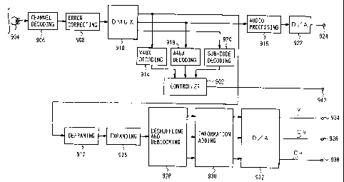
Fig. 22 is a block diagram showing the construction of a
digital VCR 106 that records a signal that is output from the PAL
plus record side processing circuit 208 according to the fourth
embodiment. A recorded luminance signal Y and a recorded color
difference signal CB/CR that are component color video signals
are supplied from input terminals 232 and 234, respectively. A
SONY(ecs)\3367.APP - 49 -
PATENT
450100-3367
helper signal is inserted into the recorded luminance signal Y in
the interval of the invalid screen portion.
The recorded luminance signal Y and the recorded color
difference signal CB/CR are supplied to a valid information
extracting circuit 324, which removes data in the interval of the
invalid screen portions (such as in the vertical blanking
interval and the horizontal blanking interval) and extracts data
in the interval of the valid screen. (Valid lines of the signal
are considered to include the "invalid" portions of the letter
box, i.e., lines 23 to 310 of field 1 and the lines 335 to 622 of
field 2; Fig. 2).
In the PAL plus system, the WSS signal that represents
the aspect ratio data, the ID signal that identifies whether or
not the helper signal is present, and so forth are inserted into
the line 23. In addition, the white 100 % reference signal is
inserted into the line 623. However, since the line 623 is not
a valid line, the white 100 % reference signal is removed. On
the other hand, although the line 23 is a valid line, the level
of the WSS signal is changed to the level of the digital value
"64" by the mute circuit 29 of the PAL plus record side
processing circuit 208.
The output signal of the valid information extracting
circuit 324 is supplied to a block segmenting and shuffling
circuit 326, which segments the extracted into (8 x 8) blocks and
SONY(ecs)\3367.APP - 50 -
PATENT
450100-3367
equally shuffles them so that the signal is equally compressed on
the screen and data is prevented from being sequentially lost due
to head clogging and tape damage.
The output signal of the block segmenting and shuffling
circuit 326 is supplied to a compressing circuit 328, which
compresses the video data corresponding to DCT and variable
length encoding methods. The compressing circuit 328 comprises a
DCT circuit, a quantizer that quantizes the DCT transformed data,
an estimator that estimates the total code amount and determines
an optimum quantizer, and a variable length encoding circuit that
compresses data corresponding to a two- dimensional Huffman code.
The compressing circuit 328, thus, converts (8 x 8) data of a
time region into (8 x 8) coefficient data of a frequency region,
guantizes the converted data, and then encodes the resultant data
into a variable length code.
The output signal of the compressing circuit 328 is
supplied to a frame segmenting circuit 330, which packs video
data in a predetermined sync block corresponding to a
predetermined rule. The output signal of the frame segmenting
circuit 330 is supplied to a VAUX adding circuit 332, which
receives VAUX data from a VAUX generating circuit 310. The VAUX
generating circuit 310 generates the VAUX data corresponding to
data received from the controller 322. Video data to which the
SONY(ecsl\3367.APP - 51 -
PATENT
450100-3367
VAUX data has been added by the VAUX adding circuit 332 is
supplied to a multiplexer 314.
The WSS data to be written to a TR pack is supplied to
the input terminal 240 from the WSS reference/encoder circuit 204
(shown in Fig. 15). The white 100 % reference data to be written
to the TR pack is supplied to an input terminal 236 from the
output terminal 224 of the PAL plus record side processing
circuit 208 (shown in Figs. 15 and 17) and is used by the VAUX
generating circuit 310 to generate the VAUX data.
In practice, the VAUX data is stored in a TR pack
(header = 66h) as shown in Fig. 37A along with the ID signal. As
described above, the WSS data is recorded in PCl to PC3 of the TR
pack, while the white 100 % reference data is recorded in PC4 of
the TR pack. When the white 100 % reference data cannot be
obtained due to any reason, (FFh) is recorded in PC4.
Fig. 23 is a schematic diagram showing a data pack
configured as a TR pack. The WSS data of 14 bits is packed from
the fifth bit of PC1 in the direction of MSB (b0, b1, b2 and so
forth). When PC1 is packed with bits, the rest of the WSS data
is packed in PC2 from LSB to MSB (b3, b4, ..., and b10).
Thereafter, the rest of the WSS data is packed in PC3 from LSB to
MSB (b11, b12, and b13). In such a manner, the TR pack is filled
with the WSS data. Since the value of the white 100 % reference
data is at most "235", it is written to eight bits of PC4.
SONY(ecs)\3367.APP _ 52 _
21~~~~~
~' PATENT
450100-3367
In addition, an audio signal is supplied to. an input
terminal 300 of an A/D converter 302, which digitizes the audio
signal. The resultant audio signal is supplied to an audio
signal processing circuit 304, which packs the audio data in a
predetermined sync block. The output signal of the audio signal
processing circuit 304 is supplied to an AAUX adding circuit 306.
The AAUX adding circuit 306 also receives AAUX data from an AAUX
generating circuit 308 under the control of the controller 322.
The AAUX adding circuit 306 adds the AAUX data to the audio data
and the resultant audio data is supplied to the multiplexer
circuit 314.
A sub-code generating circuit 312 generates a sub-code
data, which is used for a high speed search operation. The
sub-code data is also supplied to the multiplexer circuit 314.
The multiplexer circuit 314 outputs one of the video
data, the audio data, and the sub-code data to an error
correction encoding circuit 316. The error correction encoding
circuit 316 adds an error correction code to the record data and
outputs a corrected signal to a channel encoding circuit 318.
The channel encoding circuit 318 performs the "24 to 25"
conversion for the record data and encodes the recorded signal
corresponding to the partial response class 4 suitable for
digital recording. The output signal of the channel encoder 318
is supplied to a head 320 through a recording amplifier (not
SONY(ecs)\336~.APP _ 53
......
PATENT
450100-3367
shown). Thus, the record data is recorded on the recording tape
in the above-described format.
iii. Dicrital Sictnals Recorded on the Magnetic Tape
_ Figs. 24 to 27 are schematic diagrams showing levels of
signals recorded on a magnetic tape according to the fourth
embodiment. Figs. 24A-E are schematic diagrams showing the case
where the DC setup value of the DC level shift circuit 262 of the
PAL plus record side processing circuit 208 is "64". In the
signal level on the line 23 shown in Fig. 24A, since the helper
signal is inserted into the recorded luminance signal Y, the
reference signal of tie helper signal is disposed on the line 23.
Thus, the value of the reference signal is smaller than the DC
setup value "64" by "54".
Fig. 24B is a schematic diagram showing a signal level
in the interval of the invalid screen portions (namely, on the
lines 24 to 59, the lines 275 to 310, the lines 336 to 371, and
the lines 587 to 622). In this embodiment, the helper killer
function is turned off and the value of the helper signal
inserted into the interval of the invalid screen portions is at
most "108" with a center value of the DC setup value "64". The
level of the maximum value is normalized by the A/D converter
214a.
SONY(ecs)\3367.APP _ Sq _
PATENT
450100-3367
In the interval of the invalid screen portions, signals
are not inserted into the recorded color difference signal CB/CR.
Fig. 24C is a schematic diagram showing a signal level
in the interval of the main screen portions (namely, on the lines
60_to 274 and the lines 372 to 586). In this interval, the
signal levels of the resultant signals are the same as those
corresponding to the conventional PAL plus system. The maximum
value of the recorded luminance signal Y is the white 100
reference level (namely, "235") and the minimum value thereof is
the pedestal level (namely, "16"). Likewise, the level of the
recorded color difference signal CB/CR has a deviation of "112"
with a center value o~ "128" (thus, the minimum value thereof is
"16", whereas the maximum value thereof is "240").
Fig. 24D is a schematic diagram showing the level of
the signal on the three upper lines of each of the main screen
portions (namely, on the lines 60 to 62 and the lines 372 to
374). In this interval, to prevent a compression distortion in
the DCT compression method, the recorded luminance signal Y is
muted to a level "64" that is the DC setup value, whereas the
recorded color difference signal CB/CR is muted to a level "128"
(namely, an achromatic color level.).
Fig. 24E is a schematic diagram showing a reference
signal in the white 100 % level on the line 623. This signal is
SONY(ecs)\336~.APP - 55 -
450100A3367
not recorded on the tape because it is on line 623, which is
during the vertical blanking interval (Fig. 4).
Fig. 25A is schematic diagram showing the case where
the DC setup value is "32". Thus, the level of the reference
signal of the helper signal is lower than the DC setup value "32"
by ..27.. .
Fig. 25B is a schematic diagram showing a signal level
in the interval of the invalid screen portions. The level of the
helper signal inserted into the interval of the invalid screen
portions is at most "54" with a center of the DC setup value at
"32" that is normalized by the A/D converter 214a. In the
interval of the invalid screen portions, no signal is inserted
into the recorded color difference signal CB/CR.
Fig. 25C is a schematic diagram showing a signal level
in the interval of the main screen portions. In this interval,
the DC setup value of each of the recorded luminance signals Y
and the color difference signals CB and CR is the same as "64" as
shown in Fig. 24C.
Fig. 25D is a schematic diagram showing the level of
the signal on the three upper lines of each of the main screen
portions. In this interval, so as to prevent a compression
distortion in the DCT compression method, the recorded luminance
signal Y is muted to a level "32" that is the DC setup value,
SONY(ecs)~3367.APP _ 56 _
...
PATENT
450100-3367
whereas the recorded color difference signal CB/CR is muted to a
level "128" (namely, an achromatic color level).
Fig. 25E is a schematic diagram showing a reference
signal in the white 100 % level on the line 623. This signal is
not recorded on the tape, as discussed with reference to Fig.
24E.
Fig. 26A is a schematic diagram showing the case where
the DC setup value is "128". As the level of the signal on the
line 23 shown in Fig. 26A, the level of the reference signal of
the helper signal is lower than the DC setup value "128" by .
~~108" .
Fig. 26B is~a schematic diagram showing a signal level
in the interval of the invalid screen portions. The level of the
helper signal inserted into the interval of the invalid screen
portions is at most "216" with a center of the DC setup value set
to "128" that is normalized by the A/D converter 214a. In the
interval of the invalid screen portions, no signal is inserted
into the recorded color difference signal CB/CR.
Fig. 26C is a schematic diagram showing a signal level
in the interval of the main screen portions. In this interval,
the DC setup value of each of the recorded luminance signals Y
and the color difference signals CB and CR is the same as "64" as
shown in Fig. 24C.
SONY(ecs)~3367.APP _ 57 _
PATENT
450100-3367
Fig. 26D is a schematic diagram showing the level of
the signal on the three upper lines of each of the main screen
portions. In this interval, so as to prevent a compression
distortion in the DCT compression method, the recorded luminance
signal Y is muted to a level "128" that is the DC setup value,
whereas the recorded color difference signal CB/CR is muted to a
level "128" (namely, an achromatic color level).
Fig. 26E is a schematic diagram showing a reference
signal in the white 100 % level on the line 623. This signal is
not recorded on the tape, as discussed with reference to Fig.
24E.
2. EDTV-2 Embodiments
Fig. 27 depicts a block diagram of the present
invention employed in an EDTV-2 system. An EDTV-2 signal is
received by a tuner 400 and output to an input terminal 402 of an
EDTV-2 recording processor 404. The EDTV-2 recording processor
outputs a processed EDTV-2 signal to the digital VCR 106. As in
the previous embodiments, the vertical resolution component is
stored as a luminance signal Y and the related signals are stored
in a TR pack. In this manner, the vertical resolution is
restored after digital recording and a high image quality is
maintained.
SONY(ecs)\3367.APP - 58 -
PATENT
450100-3367
More specifically, the EDTV-2 recording processor 404
decodes the HH signal at the main screen portion and multiplexes
it with a luminance signal at the main screen portion. In
addition, the EDTV-2 recording processor 404 adds offsets to the
VT_and VH signals that are sent to the upper and lower invalid
screen portions so as to record them as luminance signals Y.
Moreover, the EDTV-2 recording processor 404 decodes the ID
signals sent to the lines 22 and 285 from the EDTV-2. video signal
and extracts the aspect ratio data and the data that represents
whether signal components of VT, VH, and HH are present from the
ID signals. Since the digital VCR 106 processes the EDTV-2 video
signal at a sampling frequency of 13.5 MHz, it can record the
signal in a band of around 6 MHz. The EDTV-2 recording processor ,
404 outputs component color signals Y, CR, and CB to the digital
VCR 106. The aspect ratio data, the data that represents whether
or to signal components of VT, VH, and HH are present, and color
phase information are separately supplied to the digital VCR 106.
a. Fifth Embodiment
i. EDTV-2 Recording Processor
Fig. 28 is a block diagram showing the EDTV-2 recording
processor 404 of the fifth embodiment. An EDTV-2 video signal is
supplied to an input terminal 402, which is connected to a
three-dimensional Y/C separating circuit 404. The
SONY(ecs)\3367.APP - 59 -
2~~w~~~
PATENT
450100-3367
three-dimensional Y/C separating circuit 404 separates a
luminance signal Y from a chrominance (i.e., color) signal C. In
addition, the three-dimensional Y/C separating circuit 404
extracts a multiplexed HH signal from the Fukinuki hole. The
extracted signal is supplied to an HH signal demodulating circuit
406, which demodulates the HH signal and outputs a high band
horizontal luminance component of a frequency band of 4.2 MHz to
6 MHz. The output signal of the HH signal demodulating circuit
406 is then supplied to an addition circuit 408.
The Y/C separating circuit 404 outputs a luminance
signal of up to 4.2 MHz and a chroma signal C. The luminance
signal Y is supplied to the addition circuit 408, which adds the
high band horizontal luminance component (4.2 MHz to 6 MHz
supplied from the HH signal demodulating circuit 406) to the
luminance signal Y (of up to 4.2 MHz). The output signal of the
addition circuit 408 is supplied to a terminal 410A of a switch
circuit 410.
The input signal of the input terminal 402 is also
supplied to an offset adding circuit 414, an ID signal decoding
circuit 416, and a synchronous signal separating signal 420. The
synchronous signal separating circuit 420 detects a synchronous
signal from the input signal of the input terminal 402 and
outputs the synchronous signal to a line decoder 422. The output
signal of the line decoder 422 is supplied to the ID signal
SONY(ecs)\3367.APP - 60 -
...
PATENT
450100-3367
decoding circuit 416 and a switch controlling circuit 424 for
controlling switches 410 and 412. .
The offset adding circuit 414 adds offsets to the VT
and VH signals that are in the invalid screen portions so as to
process them as luminance signals. The output signal of the
offset adding circuit 414 is supplied to a terminal 410B of the
switch~circuit 410.
The ID signal detecting circuit 416 detects aspect
ratio data and data that represents whether or not signal
components of VT, VH, and HH are present on lines 22 and 285.
The output signal of the ID signal detecting circuit 416 is
output to a data output terminal 418. The ID signal detecting
circuit 416 also controls the state of the three-dimensional Y/C
separating circuit 404 based on which signals are detected.
The switch controlling circuit 424 generates a switch
control signal for selecting one of the main screen portion and
the invalid screen portions. When the switch control signal is
supplied to the switch circuits 410 and 412, the switch circuits
select one of the main screen and invalid screen portions
corresponding to the switch control signal.
When the main screen portion at the center of the
screen is selected, the switch circuit 410 is placed in the
terminal 410A position and the switch circuit 412 is turned on.
On the other hand, when the upper and lower invalid screen
SONY(ecs)\3367.APP - 61 -
2~~~08'~
PATENT
450100-3367
portions are selected, the switch circuit 410 is placed in the
terminal 410B position and the switch circuit 412 is turned off.
Thus, the switch circuit 410 outputs the luminance signal Y, to
which the horizontal high band component HH has been added to the
main screen portion. In addition, the switch circuit 410 outputs
the vertical resolution compensating signals VT and VH; to which
offsets have been added to the invalid screen portions. The
switch circuit 412 outputs the chroma signal C to the main screen
portion. However, the switch circuit 412 does not output the
chroma signal C during the invalid screen portions.
The output signal of the switch circuit 410 is output
to an output terminal'426. The output signal of the switch
circuit 412 is supplied to a color demodulating circuit 428,
which demodulates the color difference signals CR and CB from the
chroma signal C. The color difference signals CR and CB are
output from output terminals 430 and 432, respectively. Thus,
the video component signals are sent to the digital VCR.
ii. Digital VCR Recording
The digital VCR 106 digitizes the component
color signals Y, CR, and CB, compresses them corresponding to DCT
and variable length encoding methods, and records the resultant
signals on a magnetic tape through a rotating head. When an
EDTV-2 video signal is recorded, the aspect ratio data (the data
SONY(ecs)\3367.APP _ 62 _
450100A3367
that represents whether or not signal components of VT, VH, and
HH are present, and so forth) are supplied to the digital VCR 106
from the EDTV-2 recording processor 404. These types of data are
stored as VAUX data by the digital VCR 106. At this point, the
HH_signal is decoded and restored in the band of 6 MHz. Thus,
these types of data are recorded in such a manner that the HH
signal is absent. When the digital VCR 106 records the EDTV-2
video signal, only a valid portion is extracted. The ID signal
is sent to lines 22 and 285. The line 22 is not a valid line and
is not displayed, whereas the line 285 is a valid line. Thus,
the signal on the line 285 is placed in the pedestal level in
order that the data on line 285 be hidden. Thus, these signals
are not recorded on the valid screen, thereby preventing color
reproducibility and image quality from deteriorating.
Fig. 29 is a block diagram showing the construction of
a recording system of a digital VCR 106 according to the fifth
embodiment. Component video signals Y, CR, and CB are supplied
to input terminals 444, 446, and 448, respectively. The
component color video signals Y, CR, and CB are supplied to an
A/D converter 450, which digitizes the component signals Y, CR,
and CB with a sampling clock at a frequency of 13.5 MHz. In the
case of the NTSC system, the component signals Y, CR, and CB are
digitized so that the information amounts of the luminance signal
Y and the color difference signals CR and CB are in a 4 . 1 . 1
SONY(ecs)\3367.APP - 63 -
PATENT
450100-3367
ratio, respectively. The output signal of the A/D converter 450
is supplied to a masking circuit 458.
The input luminance signal Y is also supplied to a
synchronous signal separating circuit 452, which detects and
outputs a synchronous signal to the line decoder 454. The output
signal of the line decoder 454 is supplied to a masking signal
generating circuit 456. The masking signal generating circuit
456 receives a signal from the controller 443 that identifies
whether the input video signal is an EDTV-2 video signal. When
the controller determines that an EDTV-2 video signal is input,
the masking signal generating circuit 456 outputs a masking
signal to the masking~circuit 458 for line 285.
When the EDTV-2 video signal is input, the masking
circuit 458 masks the signal on line 285 to a predetermined value
(for example, value 16 that represents a pedestal level). The
output signal of the masking circuit 458 is supplied to a valid
information extracting circuit 460, which removes data out of the
valid screen such as data in the vertical blanking interval and
horizontal blanking interval and extracts only data of the valid
screen. (The valid lines include the so-called "invalid
portions" of the letter box screen and are lines 23 to 262 of a
field 1 and lines 285 to 524 of a field 2.) In the EDTV-2
system, aspect ratio data, an ID signal that represents whether
or not signal components of VT, VH, and HH are present, and a
SONY(eca)\336'I.APP - 64 -
21~2a8~
PATENT
450100-3367
2.04 MHz confirmation signal that identifies whether the received
video signal is an EDTV-2 video signal are multiplexed on the
lines 22 and 285. However, since the line 22 is not a valid
line, the multiplexed signal on the line 22 is removed. On the
other hand, although the line 285 is a valid line, the
multiplexed signal on the line 285 is placed in the pedestal
level by the masking circuit 458, so that the vertical resolution
information on line 285 does not appear on the recovered image.
The output signal of the valid information extracting
circuit 460 is supplied to a block segmenting and shuffling
circuit 462. As in other shuffling circuits described in the
previous embodiments;'the block segmenting and shuffling circuit
462 segments the signal received from the valid information
extracting circuit 460 into (8 x 8) blocks and equally shuffles
them so that the signal is equally compressed. In this manner,
data is prevented from being sequentially lost due to head
clogging and tape damage.
The output signal of the block segmenting and shuffling
circuit 462 is supplied to a compressing circuit 464, which
compresses the video data corresponding to the DCT and variable
length encoding methods. In other words, the compressing circuit
464 comprises a DCT circuit, a quantizer that quantizes the DCT
transformed data, an estimator that estimates the total code
amount and determines an optimum quantizer, and a variable length
SONY(eca)\3367.APP - 65 -
PATENT
450100-3367
encoding circuit that compresses data corresponding to a
two-dimensional Huffman code. The compressing circuit 464
converts (8 x 8) data of a time region into (8 x 8) coefficient
data of a frequency region, quantizes the converted data, and
then encodes the resultant data into a variable length code.
The output signal of the compressing circuit- 464 is
supplied to a frame segmenting circuit 466, which packs video
data in a predetermined sync block corresponding to a
predetermined rule. The output signal of the frame segmenting
circuit 466 is supplied to a VAUX adding circuit 468.
The VAUX adding circuit 468 also receives VAUX data
from a VAUX generating circuit 470, which generates the VAUX data
corresponding to data received from the controller 443. Video
data to which the VAUX data has been added by the VAUX adding
circuit 468 is supplied to a multiplexer 472.
The EDTV-2 recording processor 404 (see Fig. 28)
supplies the aspect ratio data, the ID signal data (representing
whether of signal components of VT, VH, and HH are present), and
the color phase information to the terminal 474.
Specifically, the VAUX data is stored as a TR pack
(header = 66 h) as shown in Fig. 54. The ID signal data is
recorded in the TR pack. The aspect ratio information is
recorded as DISP (Display Select Mode) of a source control pack
(header PCO = 60h) of the VAUX data. The color phase information
SONY(eca)\3367.APP - 66 -
~1~~~~~
PATENT
450100-3367
is recorded as CLF (Color Frame Identification Code) of a source
pack (header PCO = 60h) of the VAUX data.
In addition, an audio signal is supplied to an input
terminal 476 of an A/D converter 478, which digitizes the audio
signal. The resultant audio signal is supplied to an audio
signal processing circuit 480, which packs the audio data in a
predetermined sync block. The output signal of the audio signal
processing circuit 480 is supplied to an AAUX adding circuit 482,
which receives AAUX data from an AAUX generating circuit 484
under the control of the controller 443. The AAUX adding circuit
482 adds the AAUX data to the audio data and outputs the sum to
the multiplexer circuit 472.
A sub-code generating circuit 486 generates a sub-code,
which is used for a high speed search operation. The sub-code
data is also supplied to the multiplexer circuit 472.
The multiplexer circuit 472 outputs one of the video
data, the audio data, and the sub-code data to an error
correction encoding circuit 488. The error correction encoding
circuit 488 adds an error correction code to the record data and
outputs the corrected data to a channel encoding circuit 490.
The channel encoding circuit 490 performs the 24/25 conversion
for the record data and encodes the recorded signal corresponding
to the partial response class 4 suitable for digital recording.
The output signal of the channel encoder 490 is supplied to a
SONY(ecs)\3367.APP _ 6~
2~.~~~~~
PATENT
450100-3367
head 492 through a recording amplifier (not shown) for recording
the digital signals on a recording medium.
Dicrital VCR Format
The recording processing and digital VCR have been
previously discussed. A description of the format used by the
digital VCR to record the digital signals on a recording tape
will now be set forth. While the present invention is not
limited to any particular format, two formats are presented below
which are suitably used with this invention.
Dicrital VCR Format I .
The first scheme will be described with reference to
Figs. 30-46. On the tape of the digital VCR according to the
present invention, as shown in Fig. 30A, oblique tracks are
formed. Two recording conventions used are the SD system (525
lines/60 Hz and 625 lines/50 Hz) and the HD system (1125 lines/60
Hz and 1250 lines/50 Hz). In the SD system, there are 10 tracks
per frame (in the case of 625 lines/50 Hz) or 12 (in the case of
525 lines/60 Hz). In the HD system, the number of,tracks per
frame is twice as many as that of the SD system, i.e., 20 (in the
case of 1125 lines/60 Hz) or 24 (in the case of 1250 lines/50
Hz ) .
SONY(ecs)\3367.APP - 68 -
PATENT
450100-3367
Fig. 30B is a schematic diagram showing tracks formed
on a tape of the digital VCR. On the track entering side,
a timing block for securely performing after-record operation is
disposed. This timing block is referred to as ITI (Insert and
Track Information). The ITI is used to precisely align an area
that is after-recorded.
In any digital signal recording/reproducing apparatus,
data in a particular area should be rewritten. Thus, the ITI
area on the track entering side is essential. In other words,
many sync blocks with a short sync length are written in the ITI
area. The sync blocks are assigned sequential numbers from
the track entering side. When data is after-recorded, if any of
sync blocks in the ITI area is detected, the position of the
present track can be precisely detected corresponding to the sync
block number. Thus, the after-recorded area can be determined.
Generally, the track entering side cannot be stably contacted
with the head due to imperfect mechanical accuracy. To
compensate such an imperfect mechanical accuracy, many sync
blocks with a short sync length are written to improve a sync
detecting probability.
As shown in Fig. 31, the ITI area is composed of a
preamble, an SSA (Start Sync Block Area), a TIA (Track
Information Area), and a postamble. The preamble is composed of
1400 bits and is used as a run-in for PLL that reproduces a
SONYfecs)\3367.APP _ 6g _
PATENT
450100-3367
digital signal. The SSA is used for this function. The SSA is
composed of 61 blocks, each of which is composed of 30
bits. The SSA is followed by the TIA, which is composed of three
blocks that are composed of 90 bits and stores information about
the tracks.
Within the TIA, an APT (Application ID of a Track)
(three bits), an SP/LP (one bit), a reserve bit (one bit), and a
PF (Pilot Frame) bit (one bit) are stored. The APT is an
application ID which determines the type of data structure of an
area. The PF represents a reference frame of the servo system.
Thus, the TIA is composed of six bits.' The TIA is followed by
the postamble, which is composed of 280 bits and used to provide
a margin.
A cassette that encloses a recording medium is provided
with a circuit board having a memory IC (MIC). Data written in
the memory IC guides the recording/reproducing operation of the
apparatus. In the MIC, along with information such as tape
length, tape thickness, and tape type, other information such as
TOC (Table Of Contents) information, index information, character
information, reproduction control information, and timer record
information can be stored. When the cassette tape with the MIC
works in conjunction with the digital VCR, for example, data
stored in the MIC can be used to skip to_a predetermined program,
designate the reproduction order of programs, designate a
SONY(ecs)\3367.APP _ ~p _
PATENT
450100-3367
predetermined scene for reproducing a still image (photo), and
reserve a timer record operation.
Similarly, the MIC stores an application ID, called the
APM (Application ID of MIC), in the high order three bits of the
address 0 of the MIC. The APM also defines a data structure
which can be used to .
The tracks following the ITI area are divided into
several areas as shown in Fig. 32. These divided areas uniquely
define the data structure such as the track position, sync block
structure, and ECC structure, which protects data against an
error. Each area has an application ID for defining the data
structure, i.e., application of area n defines the data structure
of an area n.
The application ID has a hierarchical structure as
shown in Fig. 33. The APT, which is the basic application ID,
defines the number of areas on a track. Within each area, AP1 to'
APn are defined. While Fig. 33 shows that the application IDs
are structured in two hierarchical levels, lower hierarchical
levels can be added. The APM, which is the application ID in the
MIC, is disposed in only the first hierarchical level. The value
of the APM is the same as that of the APT of the digital VCR.
With this scheme, the digital VCR can be operated as a
completely different product such as a data streamer or a
multi-track digital audio tape recorder. Even if one area is
SONY(ecs)\3367.APP _ 71
PATENT
450100-3367
defined, the content thereof can be defined by the application ID
of the area. Thus, corresponding to the values of the
application ID, data can be designated to video data, video audio
data, computer data, and so forth.
Fig. 34A is a schematic diagram showing a track
structure in the case that APT = 000. As shown in Fig. 34A,
areas 1, 2, and 3 are defined on a track. The areas 1, 2, and 3
define the track position, the sync block structure, the ECC
structure, which protects data against an error, and the
overwrite margin for providing gap and overwrite. Each of these
areas has an application ID that defines the data structure
thereof. The application IDs are defined as follows:
AP1 ... Defines the data structure of the area 1.
AP2 ... Defines the data structure of the area 2.
AP3 ... Defines the data structure of the area 3.
The application ID of each area in the case that the
application ID = 000 is defined as follows.
AP1 = 000 ... Defines the data structure of audio and
AAUX of the CVCR.
AP2 = 000 ... Defines the data structure of video and
VAUX of the CVCR.
AP3 = 000 ... Defines the data structure of sub-
code and ID of the CVCR.
SONY(ecs)\3367.APP _ 72 _
PATENT
450100-3367
CVCR . Home use digital video and audio signal
recording/reproducing apparatus
AAUX . Audio auxiliary data VAUX . Video auxiliary
data
_ In other words, when the digital VCR is to be used in
its normal capacity, the values of APT, AP1, AP2, and AP3 are
designated to 000, as shown in Figure 34B. In addition, the
value of APM is also designated to 000.
When APT = 000, all areas of AAUX, VAUX, sub- code, and
MIC are written in a common ~~pack~~ structure. As shown in Fig.
35, one pack is composed of five bytes (PCO to PC4). The first
one byte is a header and the remaining four bytes are data. A
pack is a minimum unit of a data group. By collecting related
data, one pack is composed.
The header of eight bits is divided into a high
order four bits and a low order four bits to form a hierarchical
structure. As shown in Fig. 36, the high order four bits are
referred to as an upper header and the low order four bits as a
lower header. In addition, by a bit assignment of data, the
hierarchical structure can be extended to lower levels.
Using this hierarchical structure, the content of the pack
can be clearly categorized and the hierarchical structure can be
easily extended. In addition, 256 spaces formed from the upper
header and the lower header are reserved for a pack header table
SONY(ecsl\3367.APP _ 73 _
PATENT
2~.62fl~g
450100-3367
along with the content of each pack. With the pack header table,
each of the above-described areas is defined. Basically, each
pack is composed of five bytes in a fixed length. However, when
character data is written to the MIC, as an exception, a
variable-length pack structure is used. This is because the
limited buffer memory of the MIC should be used efficiently.
Fig. 37A is a schematic diagram showing a data
structure of a TR pack in the case that the header byte PCO is
(66h). Although there are many types of data structures
corresponding to headers, the pack shown in Fig. 37A strongly
relates to the present invention. As shown, four bits of the
data type, which is in the second half of PC1, identify various
types of signals as follows:
0000 = VBID 0001 = WSS
0010 = EDTV-2 on line 22
0011 = EDTV-2 on line 285
0100 = No identification
Others = Not defined
The data portion of PC2 is composed of 28 bits and
successively stores data from the LSB side (namely, on the
horizontal synchronous signal side) of the data portion. Fig.
37B is a schematic diagram showing the case where 14 bits of the
WSS signal are placed in the data portion.
SONY(ecs)\336~.APP _ 7q _
PATENT
450100-3367
The audio area and the video area are referred to as an
audio sector and a video sector, respectively. Fig. 38 is a
schematic diagram showing the structure of the audio sector,
which is composed of a preamble, a data portion, and a postamble.
The preamble is composed of 500 bits that are a run-up of 400
bits and two pre-sync blocks. The run-up is used for a run-up
pattern for a PLL operation. The pre-sync is used to detect an
audio sync block. The data portion is composed of 10500 bits.
The postamble is composed of one post-sync block of 50 bits and a
guard area of 500 bits. The post-sync block is used to
acknowledge the end of the audio sector with the sync number of
the ID. The guard area is used to prevent an after-recorded
audio sector from entering the next video sector.
As shown in Figs. 39A and 39B, each pre-sync block and
post-sync block is composed of six bytes. The sixth byte of the
pre-sync block is an SP/LP ID byte. When the value of this byte
is (FFh), it represents the SP mode. When the value of this byte
is (00h), it represents the LP mode. The sixth byte of the
post-sync stores (FFh) as dummy data. The above-described TIA
area also has the SP/LP ID byte as an SP/LP flag. The SP/LP flag
is redundantly used. In other words, when the TIA area can be
correctly read, the value thereof is used. If the TIA area
cannot be read, the value of the SP/LP flag in the TIA area is
used. The six bytes of each of the pre-sync block and the
SONY(ecsI~3367.APP _ 75
PATENT
450100-3367
post-sync block are recorded after "24 to 25" conversion (that
converts data of 24 bits into data of 25 bits). Thus, the total
bit lengths of the pre-sync block and the post-sync block are as
follows:
Pre-sync block . 6 x 2 x 8 x 25 / 24 = 100 bits
Post-sync block . 6 x 1 x 8 x 25 / 24 = 50 bits
As shown in Fig. 40, one sync block is composed of 90
bytes. The first five bytes of the pre-sync block has the same
structure as that of the post-sync block. The data portion is
composed of 77 bytes and is guarded by a horizontal parity C1
(eight bytes) and a vertical parity C2 (five sync blocks). The
audio sync block is composed of 14 sync blocks per track. Since
the audio sync block is recorded after the "24 to 25" conversion
is performed, the total bit length is as follows:
90 x 14 x 8 x 25 / 24 = 10500 bits
The first five bytes of the data portion are for the
AAUX data and compose one pack. There are nine packs per track.
Numbers 0 to 8 of Fig. 40 represent pack numbers of each track.
Fig. 41 is a schematic diagram.showing pack
numbers of the AAUX data that are arranged in the track
direction. In the 525 lines/60 Hz system, one video frame is
composed of 10 tracks. In the 625 lines/50 Hz system, one video
frame is composed of 12 tracks. The audio data and the sub-code
are recorded and reproduced corresponding to the video frame. In
SONY(ecs)\3367.APP _ 76 _
PATENT
2.62088
450100-3367
Fig. 41, numbers 50 to 55 represent values of the pack header
(FFh) .
As shown in Fig. 41, as the AAUX data on 10
tracks, the same pack is written ten times. This portion is
referred to as a main area, which stores essential items such as
sampling frequency and the number of quantizing bits necessary.
for reproducing the audio signal. These essential items are
written several times in order to protect the data. Thus, even
if a horizontal scratch of a magnetic tape, a single channel
clogging, or the like takes place, data of the main area can be
reproduced.
The remaining packs are successively linked as an
optional area. In Fig. 41, these packs are linked skipping those
in the main area as with a, b, c, d, e, f, g, h, ... and so forth
in the direction of the hashed arrows. One video frame comprises
30 packs as the optional area (in the case of the 525 lines/60 Hz
system) or 36 packs (in the case of the 625 lines/50 Hz system).
Since this area is literally optional, any packs can be selected
from the pack header table for each digital VCR.
Fig. 42 is a schematic diagram showing the structure of
a video sector. The structures of a preamble and a postamble of
a video sector are the same as those of an audio sector shown in
Fig. 38. As shown in Fig. 42, one sync block is composed of 90
bytes as with the audio sector. However, the number of bits of
SONY(ecs)\3367.APP _ 77
PATENT
450100-3367
the guard area of the postamble of the video sector is slightly
larger than that of the audio sector and the video sector
contains 149 video sync blocks.
As shown in Fig. 43, the structure of the first five
bytes of the sync block is the same as those of the pre-sync, the
post-sync, and the audio sync. The data portion is composed of
77 bytes and is guarded by a horizontal parity C1 (eight bytes)
and a vertical parity C2 (11 sync blocks) as shown in Fig. 44.
The upper two sync blocks and one sync block just preceding the
C2 parity are sync blocks dedicated for the VAUX data (77 bytes
of data is allocated to the VAUX data). Video data of a video
signal (other than the sync blocks dedicated for the VAUX data
and the C2 sync blocks), which is compressed by the DCT (Discrete
Cosine Transform) method, is stored. Since the video data is
recorded after the "24 to 25" conversion is performed, the total
bit length of the video sector is as follows:
90 x 149 x 8 x 25 / 24 = 111750 bits
Fig. 44 is a schematic diagram showing a video sector
of which 149 sync blocks are vertically arranged. The 135 sync
blocks at the center portion are used for a storage area of the
video signal. BUFO to BUF26 represent buffering units. One
buffering unit is composed of five sync blocks, and one track
contains 27 buffering units. One video frame formed on ten
tracks has 270 buffering units. In other words, a valid area as
SONY(ecs)\3367.APP _ 7g
PATENT
450100-3367
an image is extracted from video data of one frame, is sampled
and shuffled so that 270 groups (one buffering unit) are formed.
Data compression is performed by DCT, quantizing, and
variable length encoding methods for each buffering unit, so as
to_determine whether or not the generated code amount meets the
target data amount or less. A quantizing step of which the
generated data amount is the target data amount or less is
determined. With the determined quantizing step, data is
encoded, and the resultant encoded data is packed in one
buffering unit.
Fig. 45 is a schematic diagram showing the structure of
a sub-code sector. Unlike the audio sector and the video sector,
a preamble and a postamble of the sub-code sector do not have a
pre-sync and a post-sync. The length of the sub-code sector is
larger than that of other sectors because the sub-code sector is
frequently rewritten for indexing or the like. Since the
sub-code sector is disposed at the last portion of a track, the
sum of deviations of the first half of the track affects the
sub-code sector. As shown in Fig. 46, the sub-code sync block is
composed of at most 12 bytes, the structure of the first five
bytes of the sub-code sync block being the same as that of the
pre-sync block, the audio-sync block, and the video-sync block.
The sub-code sync block is followed by a data portion of five
SONY(ecs)\3367.APP _ 79 _
PATENT
450100-3367
bytes. The first 10 bytes of the sub-code sync block compose a
pack.
The data portion is followed by a horizontal parity C1
of 2 bytes which protects the data portion. Unlike the audio
data and the video data, a so-called product code structure with
C1 and C2 is not used in the sub-code. This is because the
sub-code is used for a high speed search operation. Thus, it is
rare to reproduce the C2 parity along with the C1 parity. In
addition, since the sub-code is searched at a speed around 200
times higher than that of the other codes, the sync length is as
small as 12 bytes. Since the sub-code sync block is composed of
12 sync blocks per track and recorded after the "24 to 25"
conversion is performed, the total bit length of the sub-code
sector is as follows:
12 x 12 x 8 x 25 / 24 = 1200 bits
Digital VCR Format II
As shown in Fig. 47, video tracks are formed on the
magnetic tape in a similar manner to the first scheme (Fig. 30).
At the beginning of each track, an ITI area is formed. The ITI
area is followed by an audio area, a video area, and a sub-code
area. The ITI area is a timing block which an after-record
operation is securely performed. When data after the ITI area is
rewritten by the after-record operation, the ITI area is used to
SONY(ecs)\3367.APP - 80 -
~~.6~~8~
PATENT
450100-3367
precisely align the data. In the audio area, the audio data is
recorded. In the video area, the compressed video data is
recorded. The sub-code area is used for a high speed search
operation. When data corresponding to the NTSC system is
recorded, one video frame is recorded on ten tracks.
Figs. 48 and 49 are schematic diagrams showing the
structure of the audio area. As shown in Fig. 50, one sync block
is composed of 90 bytes. The first five bytes of the data
portion is a pre-sync and a post- sync. The data portion is
composed of 77 bytes (audio data of 72 bytes and AAUX data of 5
bytes). The data portion is protected by a horizontal parity C1
(8 bytes) and a vertical parity C2 (5 sync blocks). As shown in
Fig. 49, one track has 14 sync blocks. The first five bytes of
the data portion comprise a pack and is used for the AAUX data.
Figs. 50 and 51 are schematic diagrams showing the
structure of data in the video area. One sync block in the video
area is composed of 90 bytes. The first five bytes of the data
portion is a pre-sync and a post-sync. The data portion is
composed of 77 bytes. As shown in Figs. 50 and 51, the data
portion is protected by a horizontal parity C1 (8 bytes) and a
vertical parity C2 (11 sync blocks).
As shown in Fig. 51, 149 sync blocks of the video
sector are vertically disposed. The upper two sync blocks and
the two sync blocks just preceding the C2 parity are used for the
SONY(ecs)\3367.APP - 81 -
PATENT
450100-3367
VAUX data. The rest of the video sector other than the VAUX data
and the C2 parity stores video data. In Fig. 29, 135 sync blocks
at the center portion of the video sector are used for a storage
area of video signal. In Fig. 51, BUFO to BUF26 represent
buffering units. One buffering unit is composed of five sync
blocks (one track has 27 buffering units; one video frame, which
is 10 tracks, has 270 buffering units). In other words, an image
valid area is extracted from image data of one frame and sampled
in order to form 270 groups, each group being one buffering unit.
Data compression is performed by DCT, quantizing, and
variable length encoding methods for each buffering unit, to
determine whether or not the generated code amount meets the
target data amount or less. A quantizing step of which the
generated data amount is the target data amount or less is
determined. With the determined quantizing step, data is
encoded. The resultant encoded data is packed in one buffering
unit, which is five sync blocks.
Fig. 52A is a schematic diagram showing the structure
of the sub-code area, which is composed of 12 sync blocks (Fig.
52B). Since one sync block is composed of 12 bytes, one sync
block in the sub-code area is smaller than one sync block in each
of the video area and the audio area. This is because the high
speed search operation needs to be performed quickly. At the
beginning of one sync block, a pre-sync of one byte and a
SONY(ecs)\3367.APP - 82 -
(~., ~ PATENT
450100-3367
post-sync of one byte are disposed. Thereafter, ID data composed
of IDO and ID1 and IDP that is a parity for IDO and ID1 are
disposed. Thereafter, a main data area of five bytes is
disposed. Thereafter, a parity of two bytes is disposed. The
main data area stores data necessary for the high speed search
operation such as a time code (record date and time).
As shown in Figs. 52C and 52D, IDO has an F/R
flag for detecting an address in the high speed search operation.
In addition, as shown in Fig. 52C, the sync blocks SBO and SB6
each have an application ID (API3) that represents the structure
of data of the sub-code. Thereafter, an absolute track number is
disposed in the same position as ID1. In other sync blocks, as
shown in Fig. 52D, an F/R flag is disposed. Thereafter, an index
ID, a skip ID, and a photo picture ID are disposed. Thereafter,
an absolute track number is disposed in the same position as ID1.
ID1 has an absolute track number and a sync number.
As shown in Fig. 53, the auxiliary data AAUX in the
audio area, the auxiliary data VAUX in the video area, the
sub-code data, and data of a cassette with a memory (not shown)
are written as a common pack structure. One pack is basically
composed of five types (PCO to PC4). The first byte of the pack
is a header. The rest of the pack (four bytes) is data.
SONY(ecs)\3367.APP - 83 -
PATENT
450100-3367
The header has two hierarchical levels of an
upper header of four bits and a lower header of four bits.
Depending on a bit assignment of data, the header can be extended
to-lower hierarchical levels. Depending on the hierarchy, the
content of the pack is clearly categorized. The hierarchical
levels of the header can be easily extended. 256 spaces composed
of the upper header and the lower header are prepared as a pack
header table along with the content of the pack. Using the pack
header table, each area is written. Although each pack is
basically composed of five bytes, as an exception, when
characters are written to a cassette with a memory, the pack has
a variable length.
Fig. 54 is a schematic diagram showing the structure of
a TR pack of the VAUX data that stores the ID signal. In the TR
pack, the header byte PCO is 66h. A data type is composed of
four bits. The data type identifies each signal. The data type
is defined as follows:
0000 = VBID
0001 = WSS
0010 = EDTV-2 on line 22
0011 = EDTV-2 on line 285
0100 = No information
Others = Not defined
SONY(ecs)\3367.APP - 84 -
PATENT
450100-3367
When an EDTV-2 signal is recorded, as described above,
data of the ID signals on the lines 22 and 285 is stored in the
TR pack. The data portion is composed of 28 bits. The LSB of
the data portion is placed on the horizontal synchronous signal
side.
Fig. 55 is a schematic diagram showing the
structure of a source pack of the VAUX data that stores the color
phase information. In the source pack, the header byte PCO is
60h. At PC1, a color frame ID code (CLF) is stored. In the NTSC
(525/60) system, the color frame ID code (CLF) is defined as
follows:
00 = Color~frame A O1 = Color frame B
Others = Reserved
In the NTSC (625/50) system, the color frame ID code is
defined as follows:
00 = First and second fields
O1 = Third and fourth fields
= Fifth and sixth fields
11 = Seventh and eighth fields
Fig. 56 is a schematic diagram showing the structure of
a source control pack of the VAUX data that stores the aspect
ratio information. In the source control pack, the header byte
PCO is 61h. PC2 defines a display select mode (DISP).
SONYtecs)\3367.APP - 85 -
PATENT
450100-3367
Corresponding to the display select mode (DISP), the aspect ratio
is defined as follows:
000 = 4 . 3 normal
001 = 4 . 3 letter box
- 010 = 16 . 9
B. REPRODUCING
The reproducing processing of the present invention
will now be discussed. The discussion will begin with a
description of a digital VCR and end with a description of
reproducing processors for each of the embodiments.
1. Dictital Signal Reproducincr VCR
When a recorded video signal is reproduced, a digital
signal reproducing VCR first reads the digital signal from the
recording medium. Two different digital signal reproducing VCRs
will now be discussed, which are applicable to both the PAL plus
and the EDTV-2 systems.
a. Discussion of a First Digital Reproducing VCR
Next, with reference to Figs. 57A, 57B and 58, the
construction of a first reproduction side of a digital VCR
according to the present invention will be described. In Figs.
57A,B, output signals of heads 500a and 500b are amplified by
head amplifiers 502a and 502b, respectively. One of the output
SONY(eCa)\3367.APP - 86 -
PATENT
450100-3367
signals of the head amplifiers 502a and 502b is selected by a
switch 504 and output to an equalizer circuit 506. The equalizer
circuit 506 compensates various losses that take place in the
magnetic recording/reproducing operations.
- The output signal of the equalizer circuit 506 is
supplied to an A/D converter 510 and a clock extracting circuit
508. The clock extracting circuit 508 extracts a clock component
and the A/D converter 510 digitizes the output signal of the
equalizer circuit 506 corresponding to the extracted clock
component. The A/D converter 510 outputs one-bit data to a FIFO .
512 memory.
The output signal of the FIFO memory 512 is supplied
to a sync pattern detecting circuit 514. The sync pattern
detecting circuit 514 receives sync patterns of various areas
through a switch 516. The switch 526 is controlled corresponding
to the output signal of a timing circuit 524. The sync pattern
detecting circuit 514 has a so-called flywheel structure,
wherein, when a sync pattern is detected, it is determined
whether or not the same sync pattern is received after an
interval of a predetermined sync block length. When the same
sync pattern is received, for example, more than three times, it
is determined that the received sync pattern is correct so as to
maintain the integrity of the sync block.
SONY(ecs)\3367.APP - 87 -
PATENT
450100-3367
When a sync pattern is detected, the shift amount of
the FIFO memory 512 necessary for extracting one sync block from
each stage thereof is, determined. Corresponding to the output
signal of the sync pattern detecting circuit 514, required bits
are supplied from the switch 518 to a sync block fixing latch
520. Thus, the latched sync number is extracted by a sync number
extracting circuit 522 and output to the timing circuit 524.
Corresponding to the received sync number, the track position of
the selected head is obtained. Thus, corresponding to the sync
number, the switches 516 and 526 are controlled.
When the ITI sector is detected, the switch 526 is
placed in the lower position. A separating circuit 528 separates
the ITI sync pattern from the signal received from the switch
526. The ITI sync pattern is supplied to an ITI decoder 530.
Since the ITI area has been encoded, when it is decoded, each
data of APT, SP/LP, and PF can be obtained. The obtained data is
supplied to a mode processing microcomputer 532 that is connected
to an external operation key pad 534. The mode processing
microcomputer 532 designates the operation mode and so forth of
the entire apparatus and controls the entire apparatus in
association with the mechanical controlling microcomputer 548 and
the signal processing microcomputer 570 (Fig. 58).
When an A/V sector or a sub--code sector is detected,
the switch 526 is placed in the upper position. In this case,
SONY(eca)\3367.APP _ gg _
2~.~20~$
PATENT
450100-3367
after sync patterns of individual sectors are extracted by a
separating circuit 536, the resultant signal is supplied to a
"24 to 25" deconverting circuit 538 and a derandomizing circuit
540. The resultant data signal has the original data sequence of
the original PAL plus signal and is supplied to an error
correcting circuit 542.
The error correcting circuit 542 detects and corrects
an error of the data received from the derandomizing circuit 540
and adds an error flag to data that cannot be corrected. The
corrected data is the output to a switch 544.
An "AV ID pre-sync/post-sync" circuit 546 processes the
ID portions of the A/~l sectors, a pre-sync, and a post-sync. The
circuit 546 extracts a sync number, a track number, and an SP/LP
signal stored in the pre-sync and the post-sync. These signals
are supplied to the timing circuit 524. Corresponding to the
output signals of the circuit 546, the timing circuit 524
generates various timings.
In addition, the circuit 546 extracts application IDs
AP1 and AP2 and outputs them to the mode processing microcomputer
532. Corresponding to the extracted AP1 and AP2, the mode
processing microcomputer 532 determines the format of the
received video signal. When AP1 and AP2 = 000, the mode
processing microcomputer 532 determines that the area 2 is an
image data area. In this case, the digital VCR 106 is operated
SONY(ecs)\3367.APP - 89 -
PATENT
21~2~$$
450100-3367
in "normal" mode.. Otherwise, a warning operation such as an
alarming process is performed.
The mode processing microcomputer 532 compares the
received SP/LP data with that obtained from the ITI sector. In a
TIA area of the ITI area, the SP/LP information is written three
times in each sync so that it is correctly detected corresponding
to detecting scheme, such as "rule of majority" scheme. The
SP/LP information is also written into four syncs of the audio
sector and the video sector, and the determination of the SP/LP
information is again made corresponding to the "rule of
majority". Thus, the reliability of the SP/LP information is
improved. When there'is an inconsistency, the data stored in the
ITI area is used with a higher precedence.
A switch 550 shown in Fig. 58 separates the
reproduced data of the video sector into video data and VAUX
data. The video data, along with the error flag, is supplied to
a deframing circuit 552, which deframes the segmented frames.
The image data is supplied to a data compression code
decoding portion. In other words, the image data is restored to
the original data by a dequantizing circuit 544 and a
decompressing circuit 556. Thereafter, the resultant data is
restored in the original image temporal arrangement by a
deshuffling circuit 558 and a deblocking circuit 560.
SONY(ecsl\336~.APP - 90 -
PATENT
450100-3367
After the deshuffling circuit 558, the luminance
signal (Y) and the color difference signals (CR and CB) are
separately processed. These signals are restored to analog
signals by D/A converters 562a, 562b, and 562c, respectively.
The resultant signals are output from terminals 564a, 564b, and
564c.
A switch 572 separates the reproduced data of an audio
sector into audio data and AAUX data. The audio data is deframed
by a deframing circuit 574 and a deshuffling circuit 576 restores
the audio data to the original time axis. At this point, if
necessary, the audio data is interpolated corresponding to the
error flag. The resultant signal is supplied to a D/A converter
578, which restores an analog audio signal. The resultant signal
is output from an output terminal 580 corresponding to timings of
the image data and the lip sync.
The VAUX data and the AAUX data separated by the
switches 550 and 572 are supplied to a VAUX circuit 564 and an
AAUX circuit 568, respectively. The VAUX circuit 564 and the
AAUX circuit 568 perform per-processes corresponding to, for
example, a "rule of majority" process for reproducing data with
reference to the error flag. The ID portion and the data portion
of the sub-code sector are supplied to a sub-code circuit 566.
Likewise, the sub-code circuit 566 performs a pre-process
corresponding to such as "rule of majority" with reference to the
SONY(ecsl\3367.APP - 91 -
2~.5~~~~
PATENT
450100-3367
error flag. The output signals of the sub-code circuit 566 are
supplied to a signal processing microcomputer 570. The signal
processing microcomputer 570 performs a final reading operation.
With the above digital reproducing VCR, the video
components, i.e., the luminance signal Y and the color difference
signals R-Y and B-Y, are supplied to a PAL plus reproducing
processor for reconstructing a PAL plus signal.
b. Discussion of a Second Digital Reproducing VCR
Next, a reproducing operation for a signal that has
been recorded on a magnetic tape corresponding to the second
digital reproducing VCR will be described. Fig. 59 is a block
diagram showing an example of the construction of a reproducing
digital VCR 106. In Fig. 59, a reproduced signal of a head 600
is supplied to a channel decoder 602 through a reproducing
amplifier (not shown). The channel decoder 602 demodulates the
reproduced signal. The output signal of the channel decoder 602
is supplied to an error correcting circuit 604. The error
correcting circuit 604 performs an error correcting process for
the signal supplied from the channel decoder 602. The output
signal of the error correcting circuit 604 is supplied to a
demultiplexer 606.
The demultiplexer 606 demultiplexes the signal
supplied from the error correcting circuit 606 into reproduction
SONY(ecs)\3367.APP _ g2 _
PATENT
450100-3367
data in the audio area, reproduction data in the video area, and
reproduction data in the sub-code area.
The reproduction data in the audio area is supplied
to an audio processing circuit 616. AAUX data of the
reproduction data in the audio area is detected by an AAUX
decoding circuit 612. The AAUX data is supplied to a controller
622. The audio processing circuit 616 performs time axis
converting process, interpolating process, and so forth. The
output signal of the audio processing circuit 616 is supplied to
a D/A converter 618. The output signal of the D/A converter 618
is output from an output terminal 620.
The reproduction data in the video area is supplied to
a deframing circuit 608. The VAUX data of the reproduction data
in the video area is detected by a VAUX decoding circuit 610 and
is supplied to the controller 622.
The WSS data is obtained from PC1 to PC3 of the TR
pack of the VAUX data. Likewise, the white 100 % reference data
is obtained from PC4. The WSS data is output from a data output
terminal 624 and then supplied to a WSS signal encoder 810
(Fig.64). The 100 % reference data is output from a data output
terminal 625 and then supplied to a PAL plus reproduction side
processing circuit 702 (Fig. 60).
SONY(ecs)\3367.APP _ g3 _
PATENT
450100-3367
The reproduction data in the sub-code area is detected
by a sub-code decoding circuit 614. The sub-code data is
supplied to the controller 622.
The output signal of the deframing circuit 608 is
supplied to an expanding circuit 628. The expanding circuit 628
converts the compressed video signal into original video signal
in the time region corresponding to the variable length code
decoding process and the inverse DCT process. The output signal
of the expanding circuit 628 is supplied to a deshuffling and
deblocking circuit 630. The deshuffling and deblocking circuit
630 outputs the reproduced component color video signals Y and C.
The signal C is obtained by line-sequencing the color difference
signals CB and CR. In addition, the helper signal has been
inserted into the signal C.
The reproduced component color video signals Y and C
are supplied to an information adding circuit 632. The
information adding circuit 632 adds a horizontal synchronous
signal, a vertical synchronous signal, and so forth to the
reproduced component color video signals Y and C. The reproduced
luminance signal Y and the reproduced color signal C are output
from output terminals 634 and 636, respectively. In this case,
as described above, when a video signal is recorded, in the
interval of the invalid screen portions, the helper signal is
inserted into the reproduced luminance signal Y. Thus, in the
SONY(ecs)~336'7.APP - 94 -
PATENT
450100-3367
interval of the invalid screen portions, the reproduced luminance
signal Y contains the helper signal.
2. PAL plus Reproducing Processor
- a. First Embodiment
Next,~the reproducing process of the record signal (PAL
plus signal) recorded by the digital VCR 106 will be described.
Fig. 61 is a block diagram showing an example of the construction
of a reproduction side according to the first embodiment of the
present invention. A luminance signal Y that is output from a
reproduction luminance signal output terminal of a digital VCR
106 is supplied to a switch circuit 706, which is controlled by a
line counter 712. The reproduction luminance signal Y received
from the.switch circuit 706 is supplied from an output terminal
706b of the switch circuit 706 to a Y/C mixing circuit 710.
Color difference signals CR and CB that are received from
reproduction color difference signal output terminals of the
digital VCR 106 are supplied to a color modulating circuit 724.
The color modulating circuit 724 converts the color difference
signals CR and CB into a color signal C. The color signal C is
supplied to a Y/C mixing circuit 710. The output signal of the
Y/C mixing circuit 710 is supplied to one input terminal of an
addition device 716.
SONY(ecs)\3367.APP _ g5 _
~1~2f~~~
PATENT
450100-3367
The WSS signal and the synchronous signal that are
output from the digital VCR 106 are supplied to a WSS detecting
circuit 708. The digital VCR 106 reads the WSS signal from the
TR pack. The WSS detecting circuit 708 detects the WSS signal
and supplies the detected WSS signal to a WSS rewriting circuit
714. The output signal of the WSS rewriting circuit 714 is
supplied to another input terminal of the addition device 716.
An output terminal 706a of the switch circuit 706 is
connected a helper signal modulating circuit 720 through an
offset removing circuit 718. The helper signal modulating
circuit 720 modulates the chrominance subcarrier signal with the
helper signal. The output signal of the helper signal modulating
circuit 720 is supplied to a further input terminal of the
addition device 716.
Another output signal of the WSS detecting circuit 708
is supplied to the line counter 712. The line counter 712
detects a horizontal synchronous signal and a vertical
synchronous signal from the output signal of the digital VCR 106
and counts a line number of the input video signal. The switch
circuit 706b is controlled corresponding to the counted line
number. When the luminance signal is reproduced and output by
the digital VCR 106 in the interval of the invalid screen
portions, the luminance signal is output as the helper signal.
When the luminance signal is reproduced and output by the digital
SONY(eca)\3367.APP - 96 -
PATENT
450100-3367
VCR 106 in the interval of the main screen portions, the
luminance signal is output as the luminance signal YL.
The line counter 712 generates a control signal that
distinguishes the main screen portions and the invalid screen
portions corresponding to the received line number. In other
words, in the interval of the upper and lower invalid screen
portions, the output terminal 706a of the switch circuit 706 is
selected. In the interval of the main screen portions, the
output terminal 706b of the switch circuit 706 is selected. In
such a manner, the switch circuit 706 is controlled.
When the luminance signal is received from the digital
VCR 106 in the interval of the invalid screen portions, the
luminance signal is selected by the switch circuit 706 and
supplied as the helper signal to the offset removing circuit 718.
The offset removing circuit 718 removes the offset level from the
signal so that the digital VCR 106 records the signal. The
resultant signal is supplied to the helper signal modulating
circuit 720, which modulates the signal that is output from the
offset removing circuit 718. The resultant signal is supplied to
one input terminal of the addition device 716.
When the luminance signal is supplied from the
digital VCR 106 in the interval of the main screen portions, the
luminance signal is selected as the luminance signal Y by the
switch circuit 706. The resultant signal is supplied to the Y/C
SONY(ecs)\3367.APP _ 97 _
~~s~s8g
:..
PATENT
450100-3367
mixing circuit 71, which mixes the luminance signal Y with the
color signal C. The resultant signal is supplied to another
input terminal of the addition device 716.
The addition circuit 716 adds the signal received from
the helper signal modulating circuit 720, the signal received
from the WSS rewriting circuit 714, and the signal received from
the Y/C mixing circuit 710. The resultant signal is output from
an output terminal 722 so that the signal is output to a PAL plus
monitor unit or the like. Thus, the PAL plus signal recorded in
the format of the digital VCR can be reproduced and output as the
original PAL plus signal.
b. Second Embodiment
The PAL plus reproducing processor of the second
embodiment is shown in Fig. 62 and is similar to the processor of
the first embodiment. A detailed discussion of this aspect of
the second embodiment is essentially discussed in regard to the
first embodiment and will not be repeated. The difference
between the reproducing processors in the first and second
embodiments is that the second embodiment does not have a helper
modulator 720. Since the helper signal was not demodulated on
the recording side (Fig. 13), the helper signal is not modulated
on the reproducing side.
SONY(ecs)\3367.APP _ gg
2~_~~~88
PATENT
450100-3367
c. Third Embodiment
Fig. 63 is a block diagram showing the construction of
the PAL plus reproduction processing circuit 106 according to the
third embodiment. In Fig. 63, a reproduced luminance signal Y is
supplied to an input terminal 742. In addition, reproduced color
difference signals CR and CB are supplied to input terminals 744
and 746, respectively. Moreover, aspect ratio information and
data that represents whether or not the helper signal is present
are supplied to a data input terminal 748.
The reproduced luminance signal received from the input .
terminal 742 is supplied to a switch circuit 750. In addition, a
synchronous signal of~the Y input signal is detected by a
synchronous signal separating circuit 752. The reproduced color
difference signals CR and CB, which are respectively received
from the input terminals 744 and 746, are supplied to a
modulating circuit 760, which generates a chroma signal C from
the color difference signals CR and CB. The output signal of the
modulating circuit 760 is supplied to a switch circuit 762.
The output signal of the synchronous signal
separating circuit 752 is supplied to a line decoder 754, which
decodes the number of lines. The output signal of the line
decoder 754 is supplied to a switch controlling circuit and a WSS
signal generating circuit 758. The switch controlling circuit
756 generates a switch control signal for selecting one of the
SONY(ecsl\3367.APP - 99 -
2162088
PATENT
450100-3367
main screen portion and the invalid screen portions. The switch
control signal is supplied~to switch circuits 750 and 762. The
switch circuits 750 and 762 select one of the main screen portion
and the invalid screen portions corresponding to the switch
control signal. When the main screen portion at the center of
the screen is selected, the switch circuit 750 is placed in the
terminal 750A position and the switch circuit 762 is turned on.
When the upper and lower invalid screen portions are selected,
the switch circuit 750 is placed in the terminal 750B position
and the switch circuit 762 is turned off.
When the main screen portion is selected, the switch
circuit 750 is placed~in the terminal 750A position and the
signal of the input terminal 742 is supplied to an addition
circuit 764 through the switch circuit 750. When the main screen
portion is selected, the switch circuit 762 is turned on. Thus,
the chroma signal C is supplied from the modulating circuit 760
to the addition circuit 764. The addition circuit 764 adds the
luminance signal and the chroma signal. The output signal of the
addition circuit 764 is supplied to an addition circuit 766.
When the invalid screen portions are selected, the
helper signal is supplied to the input terminal 742. The helper
signal is supplied to an offset removing circuit 768 through the
switch circuit 750. The offset removing-circuit 768 removes
offsets. The output signal of the offset removing circuit 768 is
SONY(ecs)\3367.APP - 100 -
~1~~~~8
PATENT
450100-3367
supplied to a modulating circuit 770. The modulating circuit 770
modulates the helper signal and outputs the modulated signal to
an addition circuit 766.
The data received from a data input terminal 748 is
supplied to the WSS signal generating circuit 758. The WSS
signal generating circuit 758 receives the output signal of the
line decoder 754. The WSS signal generating circuit 758
generates the WSS signal for the line 23. The output signal of
the WSS signal generating circuit 758 is supplied to an addition
circuit 772.
The addition circuit 772 adds the WSS signal to the
line 23. When the WSS signal is added to the line 23, since the
reproduced signal on the line 23 is placed in the pedestal level,
the data can be correctly added. The output signal of the
addition circuit 774 is output from an output terminal 774. The
output signal of the output terminal 774 is a PAL plus video
signal. Thus, when the signal is supplied to a PAL plus TV
receiver 704 (Fig. 60), a reproduced image can be displayed on
the wide screen with a high quality.
d. Fourth Embodiment
i. PAL plus Reproduction Processor
Fig. 64 is a block diagram showing the overall
construction of an embodiment for processing a reproduced PAL
SONY(ecs)\3367.APP - 101 -
PATENT
450100-3367
plus signal that is output from the above-described digital VCR
106. An output terminal 116 of the digital VCR 106 is connected
to a line sequence interpolating circuit 806. A CB/helper signal
output terminal and a CR output terminal of the line sequence
interpolating circuit 806 are connected to input terminals 830
and 832 of a PAL plus reproduction side processing circuit 808,
respectively. An output terminal 115 of the digital VCR 106 is
connected to an input terminal 834 of the PAL plus reproduction
side processing circuit 808. A data output terminal 804 of the
digital VCR 106 is connected to a data input terminal 836 of the
PAL plus reproduction side processing circuit 808. A data output
terminal 802 of the digital VCR 106 is connected to a WSS encoder
810. The WSS encoder 810 is connected to one of input terminals
of an addition device 818.
A helper killer mode control circuit 812 is connected
to the WSS signal encoder 810 and an input terminal 838 of the
PAL plus reproduction side processing circuit 808. Output
terminals 840, 842, and 844 of the PAL plus reproduction side
processing circuit 808 are connected to D/A converters 814a,
814b, and 814c, respectively. The D/A converter 814a is
connected to a Y signal input terminal of a PAL encoder 816. The
D/A converter 814b is connected to a B - Y/helper signal input
terminal of the PAL encoder 816. The D/A converter 814c is
connected to an R - Y input terminal of the PAL encoder 816.
SONY(ecs)\3367.APP - 102 -
21~~~~$
PATENT
450100-3367
A Y signal output terminal of the PAL encoder 816 is
connected to the other input terminal of the addition device 818.
A C/helper signal output terminal of the PAL encoder 816 is
connected to a C/helper signal input terminal of a Y/C mixing
circuit 820 and a C output terminal 826 of a Y/C separating
output terminal 822. The addition device 818 is connected to a Y
signal input terminal of the Y/C mixing circuit 820 and an output
terminal 824 of the Y/C separating output terminal 822. A
composite signal output terminal of the Y/C mixing circuit 820 is
connected to an output terminal 828.
The reproduced luminance signal Y that is output
from the output terminal 800 of the digital VCR 106 is supplied
to the input terminal 834 of the PAL plus reproduction side
processing circuit 808. The reproduced luminance signal Y
supplied from the output terminal 800 is also supplied to a
synchronous signal separating circuit (not shown). The
synchronous signal separating circuit separately extracts a
vertical synchronous signal and a horizontal synchronous signal
from the reproduced luminance signal Y. The extracted
synchronous signals are supplied to a line counter that controls
the entire apparatus. The line counter counts the number of
lines.
The reproduced color signal C that is output from the
output terminal 801 of the digital VCR 106 is supplied to the
SONY(ecs)~3367.APP - 103 -
~~624~~
PATENT
450100-3367
line sequence compensating circuit 806. The resultant color
signal C is controlled and separated into a color difference
signal CB and a color difference signal CR by the line sequence
interpolating circuit 806 corresponding to the count value that
is output from the above-described line counter. The color
difference signal CB is supplied to the input terminal\830 of the
PAL plus reproduction side processing circuit 808. The color
difference signal CR is supplied to the input terminal 832.
White 100 % reference data is output from the data
output terminal 804 of the digital VCR 106. The white 100%
reference data is eight-bit digital data written to PC4 of the TR
pack (shown in Fig. 23) and supplied to the data input terminal
836 of the PAL plus reproduction side processing circuit 808.
The WSS data is output from the data output terminal
802 of the digital VCR 106. The WSS data is 14-bit digital data
written as b0 to b13 in PC1 to PC3 of the TR pack shown in Fig.
23. The WSS data is extracted and supplied to the WSS encoder
810, which encodes the WSS data so that it can be recognized by a
television receiver corresponding to the PAL plus system or the
like. The WSS encoder 810 generates a reference signal of the
helper signal. The WSS signal and the reference signal are
output at a position corresponding to line 23 and are supplied to
the input terminal 818a of the switch circuit 818.
SONY(ecs)\3367.APP - 104 -
PATENT
450100-3367
The helper killer signal received from the helper
killer mode control circuit 812 is supplied to the WSS encoder
810 and the input terminal 838 of the PAL plus reproduction side
processing circuit 808. As with the helper killer mode control
ci-rcuit 206 of the record side construction shown in Fig. 15, the
helper killer mode control circuit 812 turns off the helper
function corresponding to an external input signal (in other
words, it disables the function of the vertical resolution
compensation corresponding to the PAL plus system).
This function is especially important when a PAL
plus video signal is displayed by a PAL television receiver that
does not correspond to the PAL plus system. The aspect ratio of
the PAL television receiver is 12 . 9 (4 . 3), whereas PAL plus
has an aspect ratio of 16 . 9. When this video signal is
displayed by the PAL plus television receiver, as shown in Fig.
29A, the video signal is displayed as a letter box shape screen
in which the upper and lower invalid screen portions are
disposed. The helper signal is inserted into the upper and lower
invalid screen portions. The helper signal is displayed as an
image fault, such as color flickering on the invalid screen
portions.
In this case, the helper function is turned off by
the.helper killer mode control circuit 812. Thus, the PAL plus
reproduction side processing circuit 808 changes the level of the
SONY(ecs)\3367.APP - 105 -
PATENT
450100-3367
reproduced luminance signal Y in the interval of the invalid
screen portions to the digital value "16" (namely, the pedestal
level) and the levels of the reproduced color difference signals
CB and CR into which the helper signal has been inserted to the
digital value ~~128" (namely, the achromatic level). In addition,
the WSS encoder 810 mutes the signal on line 23, into which the
WSS signal has been inserted, to the level of the digital value
"16". Thus, the helper killer function prevents the screen fault
in the upper and lower invalid screen portions.
In addition, the helper killer function can be also
used in the case that the function of the vertical resolution
compensation corresponding to the helper signal does not
effectively work due to a particular cause, such as a bad quality
of a recorded signal that is reproduced by a PAL plus television
receiver.
ii. PAL plus Reproduction Side Processing Circuit
Fig. 65 is a block diagram showing an example of the
construction of the above-described PAL plus reproduction side
processing circuit 808. This circuit accomplishes the helper
killer function, inserts the white 100 % reference signal into
the line 623, and inserts the helper signal that has been
inserted into the luminance signal Y (when a video signal has
been recorded) into the reproduced color difference signal CB.
SONY(ecs)\3367.APP - 106 -
2~~~~~$
PATENT
450100-3367
In addition, this circuit removes the DC setup value added to the
helper signal.
An input terminal 834 is connected to a delay circuit
846, which is connected to both an input terminal 850a of a
switch circuit 850 included in a helper killer circuit 848 and a
DC level shift circuit 856. The DC level shift circuit 856 is
connected to an amplitude amplifying circuit 858 and an input
terminal 860a of a switch circuit 860. The amplitude amplifying
circuit 858 is connected to an input terminal 860b of the switch
circuit 860, and a common output terminal of the switch circuit
860 is connected to an input terminal 862b of a switch circuit
862.
An input terminal 830 is connected to an input
terminal 862a of the switch circuit 862. A common output
terminal of the switch circuit 862 is connected to an input
terminal 852a of a switch circuit 852 included in the helper
killer circuit 848. An input terminal 832 is connected to an
input terminal 854a of a switch circuit 854 included in the
helper killer circuit 848.
The helper killer circuit 848 comprises switch
circuits 850, 852, and 854. Input terminals 850b, 852b, and 854b
of the switch circuits 850, 852, and 854 are connected to
respective digital level sources. The input terminal 850b is
SONY(ec91~3367.APP - 107 -
~~~~p~$
PATENT
450100-3367
connected to a digital level source "16", and the input terminals
852b and 854b are connected to a digital level source "128".
A common output terminal of the switch circuit 850
included in the helper killer circuit 848 is connected to an
input terminal 868a of a switch circuit 868, which is included in
a white level reference circuit 864. A common output terminal of
the switch circuit 868 is connected to an output terminal 840.
An input terminal 868b of the switch circuit 868 is connected to
a register 870, and a data input terminal 836 is connected to the
register 870. A common output terminal of the switch circuit 852
is connected to an output terminal 842, and a common output
terminal of the switch circuit 854 is connected to an output
terminal 844.
The PAL plus reproduction side processing circuit
808 includes a line counter 872. The line counter 872 counts the
number of lines of the video signal corresponding to the vertical
synchronous signal, the horizontal synchronous signal (which are
supplied from the above-described synchronous signal separating
circuit (not shown)), and the system clock (which controls the
entire apparatus) and outputs the count value to the following
circuits, which are controlled corresponding to the count value:
Switch circuits 850, 852, and 854 included in the
helper killer circuit 848
Switch circuit 862
SONY(ecs)\3367.APP - 108 -
PATENT
450100-3367
Switch circuit 868 included in the white level
reference circuit 864
Instead of the line counter 872, a line counter (not
shown) that controls the entire apparatus may be used.
The reproduced luminance signal Y is supplied to the
delay circuit 846 through the input terminal 834. The delay
circuit 846 has a half clock accuracy (namely, an accuracy of the
half timing of the system clock). The delay circuit 846 corrects
the deviations of timings of the reproduced luminance signal Y
and the reproduced color difference signals CB and CR, which are
generated by the PAL plus reproduction side processing circuit
808. The reproduced luminance signal Y that is output from the
delay circuit 846 is supplied to the input terminal 850a of the
switch circuit 850 included in the helper killer circuit 848.
The reproduced luminance signal Y that is output from
the delay circuit 846 is also supplied to the DC level shift
circuit 856. The above-described recording apparatus inserts a
helper signal along with a predetermined DC setup value into the
reproduced luminance signal Y during the interval~of the invalid
screen portions. The DC level shift circuit 856 removes the DC
setup value, added during recording. .In this case, the switch
circuit 862 (that will be described later) disposed on the output
side of the DC level shift circuit 856 selectively supplies the
signal to the later stage in the interval of the invalid screen
SONY(eca)\3367.APP - 109 -
~~.62~~8
PATENT
450100-3367
portions. Thus, in the DC level shift circuit 856, even i.f the
DC level of the reproduced luminance signal Y is entirely
shifted, no problem takes place.
The reproduced luminance signal Y, from which the DC
setup value has been removed, is supplied to the input terminal
860a of the switch circuit 860 and the amplitude amplifying
circuit 858. The amplitude amplifying circuit 858 amplifies the
amplitude of the reproduced luminance signal Y so that the
amplitude thereof becomes the same as the original amplifies
thereof. For example, if the luminance signal Y is amplified
with an amplification factor of 1/2 when a video signal is
recorded, the amplitude amplifying circuit 858 amplifies the
reproduced luminance signal Y with an amplification factor of 2.
The output signal of the amplitude amplifying circuit 858 is
supplied to the input terminal 860 of the switch circuit 860.
As described above, when a video signal is recorded,
the DC setup value is designated corresponding to the
amplification factor of the amplitude amplifying circuit 858.
Thus, by detecting the level of the helper signal sent to the
line 23, the DC setup value and the amplification factor can be
obtained.
The switch circuit 860 is externally controlled
corresponding to a mode control input signal supplied from an
external source. When the input terminal 860a is selected, the
SONY(ecs)\3367.APP - 110 -
PATENT
450100-3367
reproduced luminance signal Y is directly supplied from the DC
level shift circuit 858 to the common output terminal of the
switch circuit 860 (namely, the reproduced luminance signal Y is
not amplified). On the other hand, when the input terminal 860b
is~selected, the reproduced luminance signal Y that has been
amplified is supplied to the common output terminal of the switch
circuit 860 through the amplitude amplifying circuit 858.
The reproduced luminance signal Y in which the DC
setup value has been removed and has been amplified is supplied
from the common output terminal of the switch circuit 860 to the
input terminal 862b of the switch circuit 862. The reproduced
color difference signal CB is supplied to the input terminal 862a
of the switch circuit 862 through the input terminal 832. The
switch circuit 862 is controlled corresponding to the count value
of the line counter 872. In the interval of the invalid screen
portions, the input terminal 862b is selected, and in the
interval of the main screen portion, the input terminal 862a is
selected.
In other words, with reference to Fig. 2; in the
interval of the upper invalid screen portion on lines 24 to 59,
the output terminal 862b is selected. In the interval of the
main screen portion on lines 60 to 274, the output terminal 862a
is selected. In the interval of the lower invalid screen portion
on lines 275 to 310, the output terminal 862b is selected. In
SONY(ecs)\3367.APP - 111 -
PATENT
450100-3367
the interval of the upper invalid screen portion on lines 336 to
371, the output terminal 862b is selected. In the interval of
the main screen portion on lines 372 to 586, the output terminal
862a is selected. In the interval of the lower invalid screen
portion on lines 587 to 682, the output terminal 862b is
selected. .
When the switch circuit 862 is controlled in the
intervals of the main screen portions and the invalid screen
portions, the helper signal that has been inserted into the
reproduced luminance signal Y in the interval of the invalid
screen portions is inserted into the reproduced color difference
signal CB in the inteival of the invalid screen portions. The
reproduced color difference signal CB into which the helper
signal has been inserted in the interval of the invalid screen
portions is supplied from the output terminal of the switch
circuit 862 to the input terminal 852a of the switch circuit 852
included in the helper killer circuit.
The reproduced color difference signal CR is
supplied to the input terminal 854a of the switch circuit 854 of
the helper killer circuit 848 through the input terminal 832.
As described above, the reproduced luminance signal
Y and the reproduced color difference signals CB and CR into
which the helper signal has been inserted in the interval of the
invalid screen portions are supplied to the input terminals 850a,
SONY(eca)\3369.APP - 112 -
PATENT
450100-3367
852a, and 854a of the switch circuits 850, 852, and 854 included
in the helper killer circuit 848, respectively. A digital value
"16~' is supplied to the input terminal 850b of the switch circuit
850, and a digital value "128" is supplied to the input terminals
852b and 854b of the switch circuits 852 and 854.
The helper killer signal is supplied from the helper
killer control circuit 812 to the helper killer circuit 848
through the input terminal 838. The helper killer function is
turned on and off corresponding to the helper killer signal. The
switch circuits 850, 852, and 854 are controlled corresponding to
both the helper killer signal and the count value of the line
counter 872.
When the helper killer function is tuned on, the switch
circuits 850, 852, and 854 are controlled corresponding to the
count value of the line counter 872. In the interval of the
invalid screen portions, the input terminals 850b, 852b, and 854b
of the switch circuits 850, 852, and 854 are selected,
respectively. In the interval of the main screen portions, the
input terminals 850a, 852a, and,854a of the switch circuits 850,
852, and 854 are selected, respectively.
In other words, when the helper killer function is on
and with reference to Fig. 2, in the interval of the upper
invalid screen portion on the lines 24 to 59, the input terminals
850b, 852b, and 854b of the switch circuits 850, 852, and 854 are
SONY(ecs)\3367.APP - 113 -
PATENT
450100-3367
selected. In the interval of the main screen portion on the
lines 60 to 274, the input terminals 850a, 852a, and 854a are
selected. In the interval of the lower invalid screen portion on
the lines 275 to 310, the input terminals 850b, 852b, and 854b
are selected. In the interval of the upper invalid screen
portion on the lines 336 to 371, the input terminals 850b, 852b,
and 854b are selected. In the interval of the main screen
portion on the lines 372 to 586, the input terminals 850a, 852a,
and 854a are selected. In the interval of the lower invalid
screen portion on the lines 587 to 622, the input terminals 850b,
852b, and 854b are selected.
Thus, in'the interval of the invalid screen
portions, the level of the reproduced luminance signal Y is
changed to the level of the digital value "16" supplied to the
input terminal 850b of the switch circuit 850. The resultant
signal is output from the output terminal of the switch circuit
850. The level of the reproduced color difference signal CB into
which the helper signal has been inserted is changed to the level
of the digital value "128". The level of the reproduced color
difference signal CR is changed to the level of the digital value
"128" supplied to the input terminal 854b of the switch circuit
854. The resultant signals are output from the output terminals
of the switch circuits 852 and 854, respectively.
SONY(ecs)\3367.APP - 114 -
PATENT
450100-3367
In the interval of the main screen portions, the
reproduced luminance signal Y and the reproduced color difference
signals CB and CR supplied to the input terminals 850a, 852a, and
854a of the switch circuits 850, 852, and 854 are directly output
from the output terminals thereof.
On the other hand, when the helper killer function
is turned off, the switch circuits 850, 852, and 854 are
controlled corresponding to the count value of the line counter
872. The input terminals 850a, 852a, and 854a are always
selected. Thus, the reproduced luminance signal Y supplied to
each switch circuit and the reproduced color difference signals
CB and CR into which the helper signal has been inserted in the
interval of the invalid screen portions, are output directly to
the corresponding common output terminals of the respective
switch circuits.
The reproduced color difference signal CB that is
output to the common output terminal of the switch circuit 852
included in the helper killer circuit 848 is supplied to the
output terminal 842. The reproduced color difference signal CR
that is output to the common output terminal of the switch
circuit 854 is supplied to the output terminal 844.
The reproduced luminance signal Y is output from the
common output terminal of the switch circuit 850 included.in the
helper killer circuit 848. The resultant reproduced luminance
SONY(ecs)\3367.APP - 115 -
21~24g$
PATENT
450100-3367
signal Y is supplied to the switch circuit 868 included in the
white level reference circuit 864. The white level reference
circuit 864 comprises the switch circuit 868 (which is controlled
corresponding to the count value of the line counter 872) and the
register 870.
White 100 % level reference data is supplied from the
data output terminal 804 of the digital VCR 106 to the register
870 through the data input terminal 838. As described above, the
white 100 % level reference data is eight-bit data written to PC4
of the TR pack shown in Fig. 23 when the video signal is
recorded. The white 100 % level reference signal represents the
value of the white 100 % level detected when the video signal is
recorded and is written to the register 870.
The switch circuit 868 included in the white level
reference circuit 864 selects the input terminal 862b in the
interval of the line 623 corresponding to the count value of the
line counter 872. On the other hand, the switch circuit 868
selects the input terminal 868a in the interval of other lines.
By controlling the switch circuit 868 in such a manner, the level
of the reproduced luminance signal Y is changed to the white 100
level reference data on the line 623.
In the case that the value of PC4 of the TR pack data,
which is the white 100 % reference data, is (FFh) (namely, all
bits of PC4 are "1s") when the video signal was recorded, the
SONY(ecs)\3367.APP - 116 -
PATENT
450100-3367
reference data was not written. In this case, a digital value
"213" that represents the white 100 % level is written to the
register 864. In the digital VCR 106, since the reliability of
the reproduced data is very high, even if the white 100 % level
cannot be precisely restored, a high quality image can be
reproduced to some extent.
An external mode control signal can be supplied to
the register 870 through a mode control input terminal to control
the white 100% level. When the mode control signal is supplied
to the register 870, for example, a digital value "235" is
forcedly written to the register 870.
The reproduced luminance signal Y that is output from
the output terminal 840 of .the PAL plus reproduction side
processing circuit 808, the reproduced color difference signal CB
into which the helper signal has been inserted in the interval of
the invalid screen portions and that is output from the output
terminal 842, and the reproduced color difference signal CR that
is output from the output terminal 844 are supplied to the D/A
converters 814a, 814b, and 814c, respectively. These signals are
converted into analog signals and are supplied to the PAL encoder
818.
The PAL encoder 818 includes a line sequencing circuit,
which line-sequences the reproduced color difference signals B -
Y and R - Y. The line sequenced signal is modulated and output
SONY(ecs)\336?.APP - 117 -
21'~20~~
PATENT
450100-3367
as a chrominance signal C. In the interval of the line 23, a
helper reference burst signal is inserted into the chrominance
signal C. In addition, in the interval of the invalid screen
portions, the helper signal is inserted into the chrominance
signal C. The chrominance signal C is then supplied to the Y/C
mixing circuit 820 and the output terminal 826 of the Y/C
separating output terminal 822.
The reproduced luminance signal Y is output from the
PAL encoder 818 to the input terminal 818b of the switch circuit
818. In addition, the WSS signal and the reference signal that
are output from the WSS encoder 810 disposed at the predetermined
position as the line 23 are supplied to the input terminal 818a
of the switch circuit 818.
The switch circuit 818 is controlled corresponding to
the count value of the line counter (not shown), which controls
the entire apparatus. In the interval of the line 23, the input
terminal 818a is selected. In the interval of other lines, the
input terminal 818b is selected. Thus, the reproduced luminance
signal Y supplied from the PAL encoder 818 is changed to the WSS
signal and the reference signal supplied from the WSS encoder 810
in the interval of the line 23. Thus, the reproduced luminance
signal Y is restored to the PAL plus signal into which the WSS
signal has been inserted into the line 23.
SONY(ecs)\3367.APP - 118 -
PATENT
450100-3367
The reproduced luminance signal Y, into which the
WSS signal has been inserted, is supplied from the common output
terminal of the switch circuit 818 to the Y/C mixing circuit 820.
The reproduced luminance signal Y is supplied to the output
terminal 824 of the Y/C separating output terminal 822.
The reproduced luminance signal Y and the color signal
C supplied to the Y/C mixing circuit 820 are mixed as a PAL plus
composite video signal to the output terminal 828 and reproducing
is complete.
3. Fifth Embodiment EDTV-2 Reproducing Processor
Fig. 66 is a block diagram showing the construction of
a reproducing system for an EDTV-2 system. A digital VCR 106
outputs video components (i.e., luminance signal Y, and color
signals CR; CB) to an EDTV-2 Reproducing Processor 900. The
processor reproduces an EDTV-2 signah from the video components
and outputs the reconstructed signal to an EDTV-2 TV screen 902.
a. EDTV-2 Digital Reproducing VCR
Fig. 67 is a block diagram showing an example of the
construction of a reproducing system 900 of a digital VCR 106. A
reproduced signal of a head 904 is supplied to a channel decoder
906 through a reproducing amplifier (not shown). The
construction of the digital reproducing VCR for the EDTV-2 system
SONY(ecsl\3367.APP - 119 -
2~5'~Og~
PATENT
450100-3367
is the same for the PAL plus reproducing digital VCR shown by
Fig. 59, and only a brief discussion of the digital VCR will be
repeated here.
The channel decoder 906 demodulates the reproduced
signal and outputs the demodulated signal to an error correcting
circuit 908. The error correcting circuit 908 performs an error
correcting process and outputs the corrected signal to a
demultiplexer 910.
The demultiplexer 910 demultiplexes the signal
supplied from the error correcting circuit 908 into reproduction
data in the audio area, reproduction data in the video area, and
reproduction data in the sub-code area.
The reproduction data in the audio area is supplied
to an audio processing circuit 916. AAUX data of the
reproduction data in the audio area is detected by an AAUX
decoding circuit 918 and is supplied to a controller 903. The
audio processing circuit 916 performs time axis converting
process, interpolating process, and so forth and outputs the
processed audio signal to a D/A converter 922. The output signal
of the D/A converter 922 is then output from an output terminal
924.
The reproduction data in the video area is supplied to
a deframing circuit 912. The VAUX data of the reproduction data
SONY(ecs)\3367.APP - 120 -
2la~~aa
PATENT
450100-3367
in the video area is detected by a VAUX decoding circuit 914 and
is supplied to the controller 903.
The data of the ID signals on the lines 22 and 285
is obtained from the TR pack of the VAUX data. The color phase
information is obtained from the source pack of the VAUX data.
The aspect ratio information is obtained from the source control
pack of the VAUX data. These types of information are output
from a data output terminal 940 to the EDTV-2 reproduction
processing circuit 900.
The reproduction data in the sub-code area is
detected by a sub-code decoding circuit 920 and is supplied to
the controller 903.
The output signal of the deframing circuit 912 is
supplied to an expanding circuit 926, which converts the
compressed video signal into the original video signal in the
time region according to the variable length code/decoding
process and the inverse DCT process. The output signal of the
expanding circuit 926 is supplied to a deshuffling and deblocking
circuit 928, which outputs the reproduction component color video
signals Y, CR, and CB. The reproduction component color video
signals Y, CR, and CB are supplied to an information adding
circuit 930, which adds a horizontal synchronous signal, a
vertical synchronous signal, and so forth to the reproduction
component color video signals Y, CR, and CB. The output signal
SONY(ecs)\3367.APP - 121 -
~1~~~~~
PATENT
450100-3367
of the information adding circuit 930 is supplied to a D/A
converter 932 which converts the digital signals to their analog
counterparts and outputs the converted signals to output
terminals 934, 936, and 938, respectively.
When the EDTV-2 video signal is reproduced, in this
embodiment, a luminance signal at a frequency of up to 4.2 MHz
and a high band luminance component in a frequency band from 4.2
MHz to 6 MHz are added to the reproduced luminance signal Y at
the main screen portion. The reproduced luminance signal Y at
the invalid screen portions is composed of VT and VH signals to
which offsets have been added. The aspect ratio information, the
color phase information, and the data (that represents whether or
not signal components of VT, VH, and VH are present) are output
to a data output terminal 940. Since line 22, in which the ID
signal and so forth are disposed is outside the valid screen
area, the signal on line 22 is placed in the pedestal level. On
the other hand, although line 285 is in the valid screen area,
the signal on the line 285 is placed in the pedestal level by the
masking circuit 458 (Fig. 29) of the recording system of the VCR.
Thus, the video components are ready to be reproduced into an
EDTV-2 signal.
SONY(ecs)\3367.APP - 122 - '
~~.~2~~~
PATENT
450100-3367
ii. EDTV-2 Reproducing Processor
Fig. 68 is a block diagram showing the construction of
an EDTV-2 reproducing processor 900. In Fig. 68, a reproduced
luminance signal Y is supplied to an input terminal 942.
Reproduced color difference signals CR and CB are supplied to
input terminals 944 and 946, respectively. Aspect ratio
information, color phase information, and data that represents
whether or not signal components of VT, VH, and HH are present
are supplied to a data input terminal 948.
The reproduced luminance signal received from the
input terminal 942 is~supplied to a switch circuit 950. A
synchronous signal of the input signal is detected by a
synchronous signal separating circuit 952. The reproduced color
difference signals CR and CB received from the input terminals
944 and 946 are supplied to a modulating circuit 960. The
modulating circuit 960 generates a chroma signal C from the color
difference signals CR and CB and outputs the modulated signal to
a switch circuit 962.
The output signal of the synchronous signal
separating circuit 952 is supplied to a line decoder 954. The
line decoder 954 decodes the number of lines. The output signal
of the line decoder 954 is supplied to a switch controlling
circuit 956 and an ID signal generating circuit 958. The switch
SONY(eca)\3367.APP - 123 -
PATENT
450100-3367
controlling circuit 956 generates a switch control signal for
selecting one of the main screen portion and the invalid screen
portions by controlling the switch circuits 950 and 962. When
the main screen portion at the center of the screen is selected,
the switch circuit 950 is placed in the terminal 950A position
and the switch circuit 962 is turned on. On the other~hand, when
the upper and lower invalid screen portions are selected, the
switch circuit 950 is placed in the terminal 950B position and
the switch circuit 962 is turned off.
When the main screen portion is selected, the
switch circuit 950 is placed in the terminal 950A position. The
input signal of the input terminal 942 is supplied to an addition
circuit 966 through the switch circuit 950. In addition, the
switch circuit 962 is turned on. Thus, the chroma signal C
received from the modulating circuit 960 is supplied to the
addition circuit 966, which adds the luminance signal Y and the
chroma signal C. The output signal of the addition circuit 966
is then supplied to an addition circuit 968.
When the invalid screen portions are selected, the
switch circuit 950 is placed in the terminal 950B position. The
input signal of the input terminal 942 is supplied to an offset
removing circuit 964. The offset removing circuit 964 removes
the offsets and supplies the modified signal to the addition
SONY(ecs)\3367.APP - 124 -
210208
PATENT
450100-3367
circuit 968. The output signal of the addition circuit 968 is
then supplied to an addition circuit 970.
The input data of the data input terminal 948 is
supplied to an ID signal generating circuit 958 which receives
the output signal of a line decoder 954. The ID signal
generating circuit 958 generates signals for the lines 22 and
285. In other words, the ID signal generating circuit 958
generates an NRZ signal that represents the aspect ratio, an ID
signal that represents whether or not signal components of VT,
VH, and HH are present, and a 2.04 MHz confirmation signal that
identifying whether or not the received video signal is an EDTV-2
video signal for the Iines 22 and 285. The output signals of the
ID signal generating circuit 958 are supplied to an addition
circuit 970.
The adding circuit 970 adds the NRZ signal that
represents the aspect ratio, the ID signal that represents
whether or not signal components of VT, VH, and HH are present,
and the 2.04 MHz identification signal that identifies whether or
not the received video signal is an EDTV-2 video signal for the
lines 22 and 285. At this point, since the reproduced signals on
the lines~22 and 285 are placed in the pedestal level, these
types of data can be correctly added. The output signal of the
addition circuit 970 is obtained from an output terminal 972.
SONY(ecs)\3367.APP - 125 -
PATENT
450100-3367
The output signal of the output terminal 972 is an
EDTV-2 video signal. Thus, when this signal is supplied to a TV
set corresponding to the EDTV-2 system, the reproduced image can
be displayed on a wide screen with a high quality.
Obviously, numerous modifications and variations of the
present invention are possible in light of the above teachings.
It is therefore to be understood that within the scope of the
appended claims, the invention may be practiced otherwise than as
specifically described herein.
SONY(ecs)~3367.APP - 126 -