Note: Descriptions are shown in the official language in which they were submitted.
) 94/27204 PCTIUS94/04611
21 6218~
BIAS VOLTAGE DISTRIBUTION ~Y~
RELAl~l) APPLICATIONS
This applir~*on is related to U.S. Patent Applic~tion Serial
No. 842,922 which is a coh~ ;on-in-part of U.S. Patent No.
5,124,580, which are ~ccign~ to the ~ccignpe of the present
invention.
FIELD OF lH~- INVENTION
The present invention relates to the field of logic circuits, and
particularly to bias p,,~..t;~lc within logic circuits.
10 BACKGROUND OF l~ INVENlION
The basic P~ of all emitter coupl~ logic (ECL) gates or
current mode logic (CML) gates is a dirrc~ mI lifiPr. T},ercfjlc,
there is a si~nifir~nt incentive to fine tune the operation of the
dirr~en~ mplifiPr, thus improving the operation of the overall ECL
15 or CML logic gate.
The dirr~.~..tial ~mplifi~r typically has two emitter~o~pl~
bipolar tr~ncictors; each having a resistive load coupled b~l~n their
coll~t~r and a power supply. The CGIlllllOII e~-~iLL~.~ of the tr~nCictor
pair are coupled to a current source. Both the resistive loads and
20 current source are typically c~micon~uctor resistors. However, it is
also common to utilize a bipolar tr~ncicror that is biased in its linear
region for the current source. The base of one of the ernitter-coupled
'- ` 94/27204 PCTIUS94/04614
2l62l8~
pair is couplP~ to a reference potenhal and the base of the other
emitter-coupled transistor is coupled to an input signal.
The dirr~renhal ~mplifiPr fhnction~ such that it col"l)arus the
input signal to the reference po~ l DepPn~ing on whether the
5 input signal is less than or greater than the .-_f~nce ~r,Lial, the
dir~ ;f~r steers the current est~bli~h-P~d by the current
source ~ ough one of the emitter~ou~lP~d tr~nci~tors. This current
flow causes a coll~,yvn~ing voltage drop across only one of the load
resistors. At the same time, bec~P no current flows through the
10 other t~n~i~tor~ the collPctQr of that t~n~i~tor remains at
~p~l.J~.;...~tPIy ground pO~f n~;~l, The output of the dirr~.~.,hal
r~ r is typically taken at the cnll~tor of each of the
emitter-couple ~n~i~tors~ Thus one coll~tor is always at a voltage
poh~ l coll~nding to a low logic level and the other cnll~tor is
15 at a voltage ~n~;~l colle~nd"~g to a high logic level.
As is co.lullonly known in the industry, ECL/CML gates are
desirable b~u~ they provide the fastest bipolar logic available.
However, the main drawbaclc of the ECL/CML dirr~ al ~mplifi~r
as ~c ~ ;1~ above is that they con~-J~..c the most power of
20 conventinn~l logic technolo~iP~s and can be adversely erre:cled by
~ and power supply v~n~tinnc,
One method of improving the operahon of the dirr~,ie.~.al
~mplifier described above is suggested in U.S Patent No. 5,124,580
~ccignloA to the ~cci~ne~ of the present invention. U.S. Patent No.
94/27204 PCT,'US9~/04614
2l62l8o
5,124,580 ~ecrnhes a bipolar co.~.plP ~,.or~t;~ metal-oxide
S~miron~uctor (BiCMOS) ECL/CML gate. The basic bipolar
ECL/CML gate is improved by repl~r-ing the current source
compri-cing a resistive C-pmiron~uc~r with an MOS device biased to
5 function as a current source, i.e., o~dtcd in its s~luld~on region.
Further, the two load resistors çouple~ to the emitter coupled
pair are re~l~^~i by two linearly o~-~t~d MOS devices. The MOS
devices are co~plP~d bcl-. ~n the c~ll~or of each of the
emitter-coupled pair and a power supply. Both of the gates of the
10 MOS load devices are couF'^~ to a second commQn bias ~oterltial.
The value of the load recict~nc~ for the MOS load devices is
de~.l,~ined by the second bias ~trn~;~l and the siæ of the MOS
devices. The advantage of ut~ ng a lin~ly O~dttXi MOS device
is that their ~ ~;cl;..~r~ can be easily adjusted by rh~n~;n~ the potenlial
applied to their gate, i.e., the second bias pO~r~ . In this ~ nnc-,
the effect of ~ nc such as tf~ c and power supply on the
ECL~CML logic gate output voltage can be offset by proper control
of the bias potential on the gate of the MOS load devices. U.S.
Pa~tent Ap~lir~*on Serial No. 842,922 which is the co~ t;on-
in-part of U.S. Patent No. 5,124,580 and is also ~ccignP~ to the
~Cci~np~ of the present invention, ~licrlQsps a further improve."ent to
the basic bipolar ECLICML gate. The BiCMOS ECL/CML gate
1icrlose~ in U.S. Patent Application Serial No. 842,922 improves the
line~i~y of the MOS load resistors. In one ~icrlosP~ embo~limpnt a
plurality of parallel MOS devices are coupled bcl~n the collector
of each of the emitter coupled pair and the power supply. The gates
' 94127204 PCTIUS94/04614
2162180
of each of the devices are coupled to a switching network. The
switching network de~l",ines if the gate of each of the parallel MOS
load devices are coupled to a bias polenLial or a deactivating voltage.
The parallel MOS devices are linearly biased such that the effective
5 recict~nr~ of the parallel co",bind~ion is detc.",ined by the number and
size of load devices c~upled to the bias l ol~ n~
In both of the BiCMOS ECL/CML gates as ~icrlosed in U.S.
Patent No. 5,124,580 and U.S. Patent Applir~tiQn Serial No. 842,922
it is illl~Ol~t that the MOS load devices and current sources remain
10 biased at a particular Opf ~,.I;ng point, (i.e., linear for the load devices
and C ~ for the cu~ent source). Con~u~ntly, the bias voltages
sl~rpli~ to the gates of these MOS devices needs to remain c~ncl~nt
over v~ri~tinnc due to effects of ~ d~ supply voltage and
process flucl..A~;~..c
U.S. Patent No. 5,124,580 ~ic~ ~oses a fee~b~r~ circuit for
~.~p~ ing stable bias vol~ges to the gates of the load and current
source MOS devices. The fc~JI.a~L c~ ovides bias ~c..~;~lc
such that the MOS devices remain biased at the r ,~.te o~.d~ing
points ind~ndent of n,,~- IAI ;nnC in varying o~ ~,-1 ;ng cQntlitic!nc~ In
20 ~ i*on~ the f~31.~cL circuit allows the added a Iv~l~ge of having
the ability of adjusting the voltage swing of the output of the ECL
gate.
In a large logic circuit co..l;~in;~-g many logic gates it is
desirable to provide coll.~-c~ted bias voltages to each gate. This
1 94/27204 PCT/IJS94/04611
2I62I80
would require the inrll-cit n of a fe~db~k circuit, as desrribed above,
in the design of each logic gate. However, each fee~1b~ circuit
inrlu~Ps an opP~tin~ mplifiPr and other space concllming .;i~.;ui~.
As a result, incl~Aing a fe~b~.rL circuit with each logic gate may not
5 lend itself to a space effiri~Pnt logic circuit design. In irlition, adding
the f~b ^L~- ci~n~ may bc~l..e prohibitive in some cases where
minim~l space is available.
What is needed is a space çffiriPnt means for providing bias
~t~ lC for a BiCMOS ECLJCML logic gate that cr.su.~ that
10 s~Prifir op~ ;ng points are .~;n~i~;ne~ for MOS load and current
source devices.
SUMMARY OF l~k INVENTION
The present invention d~ hes a bias ~o~n~al distribution
system. The di~ ;bulion system provides bias ~ut~ 15 to MOS
15 devices while Pml-nng the devices' o~.a~ing con~litiQns remain
cn~ over t~ c, process, and power supply n~ ;onc
Purther, bias po~ c are gen. ~ at one main loc~tion within the
logic circuit and then disLIi~u~d throughout the logic circuit to all of
the MOS devices or to bias voltage conversion circuits. Since the
20 need to provide co...l~n~ d bias l~otcnlials at local device or
conversion I t;onc within the logic circuit is el ;n~P~i space is
con~.~,~. In ~ ition~ bias voltage conversion circuits that are in
close ~ it~ to logic gates to be biased are less susceptible to
noise.
V' 94/2720~ PCT/US94/04614
216218G
The distribution system compricfs a main bias pot~r.tial
generator for providing first and second te,l,pc.~t-lle, process, and
power supply co.~ n~tçd bias pot~fr.l;~lc The main genP ~lor is
divided into two circuits. The first circuit fnf ~tfs a first bias
5 pot~ h This circuit incl~ldes a reference MOS device and a
fe~Ab~c~ circuit which provides col..l~ .~tir)n in l~,~n~ to op~ g
c~ tion fluctll~tinnc The first bias ~ten~ iS distributed and
coup~P~ to the gates of other remote MOS load devices located within
the logic circuit. The remote MOS load devices coupled to this first
10 bias po!~r.l;~l have the same resistivity as the ~f~e.lce MOS device
if they have the same size since they are biased by the same potenlial.
If the remote MOS load device is a different size, then its resistivity
is plu~llional to the resistivity of the Ic~c.~nce MOS device; the ratio
of the resistivity and the size being the same. The remote MOS load
15 devices have the added benefit of being biased such that it f..n-~!;n,.c
in~ n-l~Pnt of v~riqtir~nc in o~ ;ng con~itirnc without the added
spa~e cor.~l...;nE~ f~lb~lrL Ci~,UiLI~ at the remote l~tionc~
In one c ~ho~ nt, the ~c~ encc load compric~ps a first set of
parallel MOS .~f~lcc load devices. The gates of the parallel
20 devices are coupled to a first s~ ching n~,.~k. The switching
nelwulL either couples the gates to the first bias potpnti~l or a
deactivating ~ot~nl;~l, (VDD). A first control signal de~.lllines
which of the gates are coupled to the first bias po~nLial and hence
which of the parallel devices are on and biased in their linear regions.
25 The resic~nr~ of the "on" devices dc~.lllines the overall rçcict~nce
of the paIallel co---hin ~I;on. S~ Prtion of the resist~nre of the parallel
~ - 94J27204 PCTIUS94/04614
2l62l8o
devices also de~l,-,ines the value of the first bias potential.
This first bias PO!el I;AI is then distributed to other remote
similar sets of parallel MOS devices which provide resistive k)~ ng
to other Cil~;ui~y. The gates of the remote parallel devices are also
S co~)pl~ to s~i~ching nclwol~ having a second control signal. The
second control signal flmctionc in the same ~ n~ as the first control
signal, i.e., ~ g the resistiviq of the parallel cc nhin-l; n, Since
the l~fe.~nce parallel devices and remote parallel devices are both
biased by the first bias pote1 lial, the resistivity of the remote parallel
10 c~mhin-Atiot is equal or pl~l,ullional to the resistivity of parallel
~fe.~nec devices; depPn~linE on their relative size. The first and
second control signals de~l,line the ~,ul)ullional rP1Ationchir between
the l~e.~n~ and remote sets of pa~allel load devices and hence, the
resisdvity of the remote parallel load devices.
The second bias po~.,lial is gen~AIed in the second circuit
within the main bias pot~nl;~l gfr~At~or. First and second bias
pot~ AlC are distributed to bias voltage conversion circuits within the
logic circuit. The bias voltage conversion circuits provide bias
v~ s to ECL/CML logic gates vithin the logic circuit such that the
20 logic gates' load and cu~ent contli*onc are the same as or
~;~yullional to that of the load and current conditinnc within the main
bias ~ I;AI gen. ~1IO~. Bias voltage co,.~ iun circuits are located
relatively closely to the logic gates that they are biasing so that locally
converted bias voltages need to travel a shorter ~lictAnce than the main
25 first and second bias pot~n~i~lc As a result, locally generated bia
'- ` 94/27204 PCT/US94/04614
-
21 621 80
voltages are not as ~ p!;hle to noise.
The distribution system of the present invention also ineludes
the c~hility of varying first and second main bias voltages
~pPn~ing on process v~ri~tionc and voltage swing r~ .ncnLC
S throughsr~ edcontrolsignals. In ~ n, localconversioncircuits
have the ç~ ility of adjusting locally converted bias voltages to
select s~ific current confi:l;onc of the logic circuit it is biasing.
Finally, since cQ~ yncA~;nn for lf-pt-,.l-~, process, and power
supply v~ri~ti-ns is pe.îull"ed in the main bias po~.~ l g~n~.dluls,
10 the need for ~d~liti~-n~l opP~:~*~n~l ~mplifiPrs at local ECLICML gate
*t~ns is obviated.
BRIEF DESCRIPIION OF THE DRAWINGS
Figure 1 is a block ~ lAIII illu~l.,.l;nE~ the bias voltage
distribution system of the present invention.
Figure 2 is a block .i;~.~.. ill.. ~l.,.l;n~ the VRRG and VFFG
(N) bias voltage &~ OI~ of the present invention.
Figure 3 is a circuit SCh~ .I;r i~ l;nE a ~implified VRRG
g~ to~ biasing a remote MOS load device.
Figure 4 is a circuit Sl~l~P~ ll;e of a VRRG gc . ,i.~or having the
20 capability of adjusting the VRRG bias voltage by s~i~ting PC control
codes.
" ') 94127204 PCT/US94104614
-
21 621 80
Figure 5 is a circuit sc~ ;c of a remote resistive load
networlc having t7.1e ~p~hility of s~lf~in~ effective device size by
;ng RC control codes.
Figure 6 is a cimrlifif~ circuit ~ I;r of a VFFG gen~,d~or
5 and Vl~ converter of the present invention coupled to a BiCMOS logic
gate utili7in~ MOS devices for loading and for its current source.
Figure 7 is a ~h'~ ' of a VFFG genP <.~o~ of the present
invention having the Ç~hjlity of adj~,~ling the value of VFFG bias
voltages ~l~ugh control code PC.
Figure 8 is a ~.h.. ~;r of a Vn converter of the present
~n having the r~p~biliq of ~7P~-~ing dirre c~ resistive loads
llu~u~}~ the RC2 code and dir~e.~t values of VFFG and V(L) through
the VC code.
Figure 9 is a 5,`l~f ~-~I;c of a BiCMOS logic gate as ~7i~losed
in U.S. Patent ApFlir~tion Serial No. 842,922 baving a parallel
PMOS load n.,.wvlL and ill..cl.,.l;n~ how V~ and VRR bias voltages
are coupled to it.
DETAILED DESCRIPIION
In the following d~ ;0~, a bias ~ot~r.l;~l distribution
20 systcm is ks.-~;be~ in which nu~l~e~lls specific details are set forth,
such as spe~ific con~uc~ivity types, circuit configurations, etc., in
" ') 94/27204 PCT/US94/04614
21 621 8a
order to provide a thorough understq-n~iing of the present invention.
It will be obvious, however, to one skilled in the art that these
CF~ific details need not be employed to practice the present invention.
In other inct-qnl~s~ well-known SLIuC~ul~S and circuits have not been
5 shown in detail in order to avoid ~ c cc~lily obsc~ g the present
n.
The present invention is a bias po~ 1 distribution system
that provides bias porr..l;~lc to many ECL/CML gates within a logic
circuit. These ~t ..t;~lc~ are g~...""t~,d in a central lo~qtinn and are
10 ~e~ , power supply and process V~.;ZI;Oll cv...~c~t~1 In
i~ n, the system includec the flexibility to externally contrvl and
scale voltage swing values and power riiccirq*Qn l~u~e,lJ~.~ts for
individual ECL/CML logic gates within a logic circuit cor.~;cl;ng Of
many ECLICML gates.
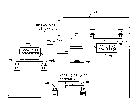
Figure 1 shows the bloclc diagrrqm of a logic circuit 83 having
the bias pot~ .I;ql riictribution system of the present i~ Livn. As can
be seen main bias voltage g".. ,.to~ 60 is located in a single locqtion
within logic circuit 83. Bias voltage gC-C ~OI 60 provides ~f~nce
bias volt~Ps, VRRG and VFFG, which are ~ lJIe~ power
20 supply and 1~lOCCS5 Vrqri-q-tioll comren~qt~d These l~fe~nce voltages
are ~ ~ onto bus 90 and coupled to many local bias converters
61 - 63 distributed throughout circuit 83. The local bias converters
L,~lsr~ the VFPG and VRRG bias volt ges into the two bi s
t;qlc~ VRRl - VRR4 and Vn, which then can be utilized to bias
local ECL/CML gates 64 - 69 on lines 91 - 96.
- 2162180
. .
PCTIUS94/046 14
46 Rec'd PCT/PT~ 22MAYl995
In addition. VRRG is distributed to and biases remote parallel
load devices 70 within logic circuil 83
Figure 2 shows the block diagram of the refe.~.~e bias voltage
gel~.at()r 60. Generator 60 is comprised of the VRRG bias voltage
gell~.àtor 100 and N VFFG bias voltage gel~.atol~ 101 - 103, where
N is- an integer greater than or e4ual to 1 VRRG is o~ d by
gen~.àtol 100 onto lines 104 and 105. Line 104 is coupled directly
to bus 90 and is then distributed to local bias g~ aLul~ 61 - 63 and
resistive loads 70 VRRG is also coupled to all of the VFFG bias
voltage ge.l~.dtol~ on line 105 and contributes in the ge.~e.d~ion of the
VFFG bias voltages The VFFG bias voltages are o~ ed onto
lines 106 - 108 and coupled to bus 90 to be distributed to local bias
co~,.t~.~ 61 - 63
The ~RG Ce.~.dtor
To illustrate how the bias distribution system of the present
invention functions to provide bias voltages to remote load devices,
the main VRRG bias genc.dtor and a single load device are shown in
a simplified embodiment in Figure 3
As can be seen, main ~RG gen~.dtol 100 is shown
co~ liaing a single PMOS device 199 of a specific size X. The drain
of 199 is coupled to a current source IREF1 and to the positive input
of operational arnplifier (OP AMP) 153 Current source IREF1 is
also coupled to a first power supply, VSS The negative input of OP
AMP 153 is coupled to reference potential VREF1 The source of
A~lENDEn SHEET
21 62I 80
PCTIUS94/046 14
12 46 Rec'd PCT~ i C 2 2-MAYl995
199 is coupled to a first power supply VDD.
Generator 100 functions such tnat OP AMP 153 generates bias
voltage, VRRG, in response to dirr~ ces between its negative and
positive inputs. In other words, OP AMP 153 generates VRRG so as
S to bias device 199 such that its drain is at the same pot~lLial as
VREF1 with a source-to-drain current of IREF1. By forcing device
199 to have specific current and voltage cha~ irs (in its linear
region), device 199 is being biased to have a cor~t ~sislivily. The
resistivity of device 199 is dependent on the values of VREF1 and
IREF1. If any ch~nges in Ope~aLi~ conditions occur, VRRG adjusts
itself accordingly so as to rn~int~in the opeldLillg point of device 199.
Utilizin~ VRRG to Bias Remote Resistive Loads
After VRRG is gel~dl~d in one central location, i.e., in main
bias voltage ge.~.ator 60, it is di~llil~u~d to tne gates of remote MOS
load devices 70 via bus 90. Figure 3 illustrates VRRG being coupled
to the gate of remote PMOS load device 198. The source of device
198 is coupled to VDD and its drain is coupled to any cil~;uill~ that
may utilize or require some type of l~ ive loading. If remote
device 198is the same size as lef~ ce device 199 then VRRG biases
both devices 198 and 199 to have the same conductivity. In the case
where the sizes of 198 and 199 are dirr~.en~, having some
proportional relationship, then the conductivity of device 198 will also
have the same proportional relationship with the conductivity of device
199. The remote devices are unaffected by flllrtll~tions in operating
~ENOE~ SHEET
2l62l8o
~TilT ~4,'d4. ~14
13 46 Rec'd PCT~P 1~, 2 2~AY1995
conditions since VRRG is adjusted so as to compensate itself for
changes in o~e~àtillg condit;on.
As shown in Figure 3, VRRG may be distributed on line 91 to
many other MOS load devices located throughout the circuit in~lir~d
by L1 - L3. Similar to device 198, the conductivity of load devices
L1 - L3 depend on their size.
Adjustable VRRG Generàtor
As noted above, the value of VRRG is set by the device size
of 199 and the values of IREFl and VREF1. However, it may be
desirable to adjust VRRG to account for variations in the voltage and
current chara~ iaLics of MOS devices due to m~mlfartllring process
flllc~l~tions. Figure 4 illuaLldt~s a VRRG main bias gel~.ator that is
not L~Llicted to a single value of VRRG.
As shown, the l~feleilce load device 198 shown in Figure 3 is
replaced by a set of parallel PMOS devices 117 - 120, (co~ osile
device 199'), having their sources coupled to VDD and their drains
coupled to the positive input of OP AMP 153'. The positive input of
OP AMP 153' is also coupled to IREF1. The negative input of OP
AMP 153' is coupled to VREF1.
The gates of devices 117 - 120 are coupled to a awitch~g
network colll~lish~g CMOS inverters 113 - 116 through lines VRR(0)
- VRR(3). The inputs of inverters 113 - 116 are controlled by process
A~ENDEO S~fEr
_ 21 621 80
, . ", ~
PcTIUS94/046 14
14 e.~ - 2~;
control signals. PC(0) - PC(3). The output of amplifier 153', which
supplies VRRG. is coupled to the CMOS ~witchhlg network, along
with VDD.
The C~OS ~wilching neLwo~l~ provides a digital ~.~ilchi~g
means to control and drive PMOS load l1clwolk 117 - 120. The gates
of devices 117 - 120, lines VRR(0) - VRR(3), are switched to either
VDD (device "off" voltage) or VRRG (device "on" voltage),
dependin on input code PC(0) - PC(3). Devices that are biased "on"
by ~RG comribute to the total linear con~ t~nre of the PMOS
net~vorl~. In other words, PC(0) - PC(3) ~etP~ ninP the effective size
and con-hlct~nre of the PMOS networlc.
VRRG gel~,dtor 85, functions in the same ll,an~r as the
simplified VRRG ge~.dtol shown in Figure 3. Specifically, once the
effec~ive size of colllposiLe device 199' is set by control signals PC(0)
- PC(3), then VRRG ge~ s a bias voltage so as to decrease the
dirr~lence bettween its positive and negative inputs. In doing tnis, OP
AMP 153' supplies a bias voltage so as to force composite device
199' to have current and voltage chalact~ ics ~t~ f.tl by VREF1
and IREF1, depending on tne size of composite device 199'.
- Thus, tne PC signal can adjust VRRG by sel~cting the errcc-ivc
size of composite device 199'. Recognize tnat composite device 199'
rnay colll~lise any nurnber of devices. Furthermore, devices 117 -120
may all be of the same size, or may be implem~nt~d as a combination
of different relative device sizes. Figure 4 shows tne currently
A~AENOED SltEET
21 621 80
4 ~ ~j 4
46 Rec'd FCT/P ~ c 2~MAY19
p~cfe~lcd device size combination wherein device 120 has a fLlced size
(denoted as size = X), device 119 has a size 2X~ device 118 has a
size 4X, and device 117 has a size 8X larger than device 120. This
particular combination of device sizes provides the user with equal
S increments of 16 different lc~ re values and 16 different VRRG
values.
As described above, VRRG can then be distributed to the gates
of other remote load devices within a logic circuit so as to bias them
in the same ll~ , or propollional to COlllpOSi~c device 199'.
10 However, instead of coupling VRRG to a many remote loads each
co~ g a single device as illustrated in Figure 3,VRRG may be
coupled to many remote loads col.l~lising a parallel PMOS load
c~wull~ similar to composite device 199' shown in Figure 4.
Figure 5 shows a remote lc~ ive load conl~lising a set of
15 parallel PMOS devices, i.e., composite device 198'. Composite
device 198' is coupled to a CMOS switching nclwol~130. Although
~clwol~130is not shown in detail, it is to be understood that it
f~lnrtion~ in the same lllal~r as the CMOS switching ne~wol~ shown
in Figure 4.
Control signals RC(0)-RC(3) control the effective size of
composite device 198' by causing ~wi~cl~iLlg nelw~ 130 to couple
either VRRG ("on" voltage) or VDD ("off" voltage) to lines
VRR(0)-VRR(3).If the sell cte~ size of 198' is the sarne as 199' then
device 198' and 199' will be biased to have the same resistivity. If
~IG~D S~
2162180
PCTIUSg4/046 14
16 46 Re~'d P~T~P i ~, 2 2MAYl995
their sizes are different then their conductivity will have the same
propor~ional relationship as the proportional relationship between
composite device sizes 199' and 198'.
As with the VRRG ge.~-ato~ shown in Figure 4, the device
sizes are scaled so as to provide the user with equal increments of 16
dirre,~ resistance values.
~s can be seen, the present invention allows on-line
adjustments of bias voltage VRRG by c~ngin~ the PC code. Also,
the ratio bet~een the RC and PC codes along with the l- f~ ce bias
curreM and voltage, de~ k the conlll]ct~nre of the remote device.
The VFFG Gcl~ tor
To illustrate how the bias distribution system of the present
invention functions to provide bias voltages to remote logic gates,
main VFFG bias gen~.dtor 103, local Vn and VRR bias co~ elh. 61,
and logic gate 64 are shown in simplified forms in Figure 6.
~lain VFFG gene-dtol 103 is shown COlll~ iilg two PMOS
devices. 200 and 201, coupled in series. The source of PMOS
devices 200 is coupled to VDD and its drain is coupled to the ~ega~ive
input of OP A~IP 1~4. The drain of PMOS device 201 is coupled to
an ~MOS device 141. The gate of device 141 is coupled to its drain.
The source of device 141 is coupled to VSS.
Device 200 is biased by VRRG and device 201 is biased by the
AMENDED SHEET
`~ 94/27204 PCTIUS94/04614
2162180
output voltage of OP AMP 154, VFFG(N). The positive input of OP
AMP 154 is co~lplPd to VL(N) The relative device sizes of 200 and
201 are such that device 201 is typically much wider that device 200
VRRG biases device 200 in its linear region having some resistivity
S det~lluned by its size and VRRG.
VFFG Gen~ lor 103 functionc such that OP AMP 154
gr~-. .,.t-~ 5 bias voltage, V~FG, in responce to dirr~.., ces b~.~.xn its
negative and positive inputs. Bias voltage, VFFG, biases device 201
in its c ~",";,~ region such that it Ç~ cl;ons as a current source The
10 current that VFFG forces device 201 to ger,~.~le is such that the
nc&dLi~. input of OP AMP 154, (node 142A) is at the sarne voltage
pQt~ r.l;~l as OP AMP 154's positive input, i e., VL(N) The current
e~n ~ ~ by device 201 is the current l~uir~d by device 200 to force
its drain voltage to equal the logic swing voltage VL(N)
Device 141 has a nPgligible affect on the VFFG g~n~ ~to- and
only fllnrtionc to est~blich the same circuit con~i~ions as in other
related circuits to be desc~ibed-
As with the VRRG gen- ~or, if any nh~ng~5 in ope.dLing
c~n~ nc occur, OP AMP 154 l~,~nds by adjusting VFFG so as to
bias device 201 such that node 142A is ~inl;~inPd at a voltage
pot~,.lial equal to VL(N)
- ~ 2162180
I'CTIUS94/046 14
18 ~ 2 ~ Yl995
Convertin~ VFFG and VRRG to Bias Volta~e. V~,
Figure 6 shows a local bias converter 61. It is to be
understood that although only a single local bias converter is shown
in Figure 6, many local converters may be distributed throughout a
5 logic circuit and coupled to main VFFG and VRRG gel~dtol~.
As can be seen in Figure 6, bias voltages VRRG and VFFG
are coupled to the gates of device 202 and device 203, re~clivt:ly.
VMG biases device 202 -in its linear region such that it functions as
a resistive load having some resistivity. VFFG biases device 203 as
10 a current source such that it establishes a current though devices 202,
- 203 and 241 having a specific current density established by the
feecib~ck circuit in the VFFG ge,~dtor circuit 103.
Note that the device size ratio for devices 202 and 203, in
local converter 61, is the same as that of devices 200 and 201, in
15 VFFG ge~ dtor 103. Since the same ratio exists benveen devices
2001201 and 202/203, and since the current established through both
sets of devices is r~ d by VFFG(N), the culTent density
established through both sets is the same. As a result, the voltage
potential at node 142B in local converter 61 is the same as the voltage
20 potential at node 142A in the main VFFG gen~ator, i.e., VL(N).
Device 241 is configured similar to device 141 of VFFG
ge,~lator 103. Specifically, device 241 is configured as half of a
current mirror. When the gate/drain node of device 241 is coupled
to the gate of another device having the same size, that other device
IDE~ SHEEt
2162180
r
-9 ~6 Rec'd P~ 2~MAYl99
will be biased lo have the same current as device 241. The gate/drain
node potential of device ~41 is referred to as V~l.
Utilizina V;~ and VRRG to Bias a Remote Lo~ic Gate
A simplified remote logic gate 64 is shown in Figure 6. As
S can be seen, it co~ ises PMOS load devices 20~4 and 205 coupled to
emitter coupled pair 21 and 22. The ernit~er~ of device 21 and 22 are
coupled to the drain of NMOS device 24. The source of device 24 is
coupled to VSS. Load devices 20~ and 205 are the same size and are
biased in their linear region and provide the load l~ e for the
10 logic gate. CulTent source device '4 is biased in its saturation region
such that it provides a constant current.
Bias voltage VRRG provides the bias voltages to load devices
204 and 205 and bias voltage V~l provides the bias voltage to current
souroe device ~4. Refel~ g to Figure 6, VRRG is coupled to the gate
of each of devices 204 and 205 and Vll is coupled to the gate of
device 24.
Since device 24 is the same device size as device 241, V~l
biases device 24 to gene.ate the same current through it as device
241. And, since load devices 204 and 205 are the same size as device
20 202, the co~ yonding voltage drop across each of them will be the
same for the same current generated by current mirror devices 24 and
241. Therefore, the low logic voltage potential at nodes 30 and 31 in
logic ~ate 64 will be the same as node 142B in remote generator 61.
The potemial established on 142B is also the same as the pol~,llial
25 established at node 142A~ i.e.. VL(N).
AUENDED ~HE;-
2162180
~CT~I~ 9 4 / ~ 4 6 14
20 41~ ~c'd PCT,~ ,T~_ 2 2 I~AYl9~S
In other words, node 30 will be at a potential equal to VL(N)if Vin significantly exceeds Vbias and node 31 will be at a potemial
equal to VL(N) if Vbias exceeds Vin. As can be seen, VL(N)
~l~tr-...i..~s the voltage swing of logic gate 64. In addition, if the
5 lcs;~ re of device 202 is made to be the same as the resi~t~n~e of
load devices 204 and 205, VL(N) is unaffected if the load resict~nre
of the logic gate is changed or varied.
Since bias voltages VRRG and VFFG are adjusted when
flllrtn~tions in o~e,.d~ g conditions occurs, Vll is correspondingly
10 adjusted so as to ensure that the voltage swing of the logic gate does
not vary.
Adjustable VFFG Gcl1~.ator
Figure 7 illu~dtes a VFFG gcn~dtor that has the added
flexibility to adjust the bias voltage VFFG independent of a specific
15 process code. This is accomplished by varying the effective device
sizes of composite devices 200' and 201'.
Refe~l;ng to Figure 7, ~witchi~g l~C~W~ i 131 couples either
VRRG or VDD on lines VRR (0) - VRR(3) to the gates of devices
133 - 136. This is done by selecting the process control signal PC(0)
20 - PC(3). Thus, control signals PC(0) - PC(3), ~e~nninP the device
size and resistivity of co~ osile device 200'. Similarly, ~witchillg
network 132 couples either VFFG or VDD to lines VFF(0) - VFF(3)
(i.e.. the gates of devices 137 - 140). This is accomplished by
A~ENDED SHEET
2162180
~CTUS94/046 14
21 4~ Rec'~ PC ~ 22~,AYl995
selecting process control signals PC(4) - PC(7) Thus, PC(4) - PC(7)
determine the device size of composite device 201'
OP AMP 154' functions to gel~.ated bias voltage VFFG in
response to dirr~rences on its input as described previously for the
5simplified VFFG generator in Figure 3 Bias voltage VFFG biases
composite device 201' such that node 142A' is equal to voltage swing
pot~llLial VL(N).
As can be seen, by adjusting device sizes of composite devices
200' and 201', VFFG will change acco-dingly, as will the current
though devices 200' and 201' However, the voltage poten~ial at node
142A' will always be forced to VL(N)
As described above, a single VFFG bias voltage is gen~lated
having an associated voltage swing potential, VL(N). However, in
certain applications it may be useful to have the capability to be able
to select from many voltage swing values As can be seen in Figure
2, main bias voltage ge~ tor 60 of the present invention generates
many VFFG bias voltages each having an ~oci~d voltage swing
lefe~ ce, VL(N). A dirrel~nt VL(N) is coupled to each VFFG
g~ to~ on lines 109 - 111 so as to gen~.~te a different VFFG on
lines 106 - 108. Each of these VFFG bias voltages along with VRRG
may then be coupled to multiple local bias COllV~.tC-~ 61 so as to
generate a Vn that forces a voltage swing potential, VL(N), for that
particular VFFG.
A~IENDED SHEET
2I62I80
, . . .
iCTIUS 9 4 / O 4 6 14
46Re~'dPCTlPTe~ 2~MAYl995
Figure 8 shows an embodiment of a local bias converter which
is -coupled to the multiple VFFG signals coupled from main bias
ge~ ator 60. The local converter has the capability of selectin~ one
of the VFFG bias voltages and its associated VL(N). Rer~ lg tO
5 Figure 8, a multiplexer, MUX 300, is shown having eight inputs,
VFFG(0) - VFFG(7). Each of bias voltages VFFG(0)-(7) functioning
to bias CGlll~osil~ device 203' so as to force a different VL(N) value
at node 142B'.
Control signals VC(0) - VC(2) ~e~ o which VFFG(N) is
coupled to input 153 of switching n~:~wolk 144. For i.. ~l~nre, in one
embo~im.ont if VC(0) - VC(3) is "000" then bias voltage VFFG(0) is
selected.
Switching ~lwol~ 143 and 144 function the same as
previously described ~wilchi-lg n~wol~. Network 143 couples either
VRRG or VDD to the gates of devices 145 - 148 on lines VRR(3) -
VRR(O). Control signals PC(0) - PC(3) select the effective device
size of colllposile device 202' and consequently its conductivity.
Switching l1~lwol~ 144 couples either the select~d VFFG or VDD to
the gates of devices 149 - 152 on lines VFF(3) VFF(0). Control
20 signals PC(0) - PC(3) select the errecliv~ device size of composite
device 203 ' and consequently the current flowing through devices 202 '
and 203'.
If the ratio between colllposile devices 200'/201' (shown in
Figure 7) and 202'/203' (shown in Figure 8) is the same then the
A~ENDED ~HEET
2162180
~, ,,, ~
PC~IU~ , ~ / 0 4 6
23 4~ Rec'd PC~ ~MAYl99
voltage potential al node 142B' in the local bias converter (Figure 8),
is the same as the voltage potential at node 142A' in tne main VFFG
generator (Figure 7), i.e., VL(~). As can be seen, the local bias
converter in Figure 8 allows for selection of a particular VL(N) with
the VC code. Conceq~lently? the Vll supplied by the local bias
converter forces the current device in the logic gate to gel~.d~t: a
current such that the voltage swing of that logic gate is the selecte~
VL(N).
Figure 9 illustrates a BiC~IOS logic gate as described in U.S.
Patent Application Serial No. 842,922. The logic gate comprises two
PMOS load networks each colllylisillg four parallel PMOS devices 71
- 74 and 75 - 78. The drains of all of ~he devices are coupled to
VDD. The sources of devices 71 - 74 are coupled to the collector of
- NPN device 21, (node 30) and the sources of devices 75 - 78 are
coupled to the collector of ~PN device 22. (node 31). Their gates are
coupled to bias voltages VRR(0) - VRR(3) as illustrated. The e.llilhLs
of devices 21 and 22 are coupled to the drain of NMOS device 24.
The source of device '4 is coupled to VSS and its gate is biased by
vn.
The bias voltages, V,I and VRR, that are utilized to bias the
logic gate shown in Figure 9 are ge~ ted by a local bias converter
such as shown in Figure 8. The voltage that biases parallel devices
145 - 148, VRR(0) VRR(3! (Figure 8!, is also coupled to the gates of
load devices 71 - 74 and 75 - /8 (Figure 9). As a result, the load
devices of the logic gate have the same resistivity as composite device
AMENDE~ S~E:T
2162180
. .
PCTIUS 9 4 / 0 4 6 14
24 ~ 22 i ~,-1995
202'. Further, the current flowing through composite device 202' is
the same as the current flowing through the logic gate's load devices
since V" is biasing device 24. Therefore, the voltage at node 30 and
31 (Figure 9) is the same as the voltage at node 142B' (Figure 8).
S As can be seen, bias voltages VRR and Vll are derived from
main bias voltages VRRG and VFFG. Consequently, if VRRG and
VFFG are co~ .,nsaLt d when variations in Op~la~ g conditions occur,
then VRR and Vl~ will also be adjusted accoldu~ly.
The resistive load values for the logic gate shown in Figure 9
may be seltocted by selecting an applol,liaLe control code PC(0) -
PC(3) while still m~int~ining the same V(L) value. In addition, logic
swing and current may be selected for the same gate by selecting the
desired VC code.
It should be noted that a logic circuit may contain many local
bias converters, each coll~/e.L~. may be set so as to provide different
loading and voltage swing conditions. Thus, the present invention
offers an extremely flexible bias distribution system. And, since local
coll~ are located in close proximity to logic gates, sensitive V~
bias voltages travel shorter ~ n~es so tnat they are less ~usce~lible
to noise.
It can also be seen that the distribution system of the present
invention is able to supply co...~ ted bias voltages to remote logic
gates with minim~l additional circuitry while still m~int~ining the
AAAENDED SHE~7
2162180
,
PCTlllS94/046 14
c 46 Rec~d PC ,T,~T~- 2 2 MAY1995
advantages of the invention as disclosed and claimed in U.S. Patent
No. 5,124,580 and U.S. Patent Application Serial No. 842,922. In
addition, the distribution system jgi-es the flexibility to adjust bias
voltages to compensate for process Yarialions ~hrough control signal
S PC in the VRRG generator.
Finally, the present invention provides a flexible distribution
system that can be tailored to particular power and logic swing needs.
~,~r~