Language selection

Search

Patent 2162211 Summary

Third-party information liability

Some of the information on this Web page has been provided by external sources. The Government of Canada is not responsible for the accuracy, reliability or currency of the information supplied by external sources. Users wishing to rely upon this information should consult directly with the source of the information. Content provided by external sources is not subject to official languages, privacy and accessibility requirements.

Claims and Abstract availability

Any discrepancies in the text and image of the Claims and Abstract are due to differing posting times. Text of the Claims and Abstract are posted:

  • At the time the application is open to public inspection;
  • At the time of issue of the patent (grant).
(12) Patent Application: (11) CA 2162211
(54) English Title: DUPLICATED ARRANGEMENT FOR ATM SWITCHING SYSTEM
(54) French Title: INSTALLATION DOUBLE POUR SYSTEME DE COMMUTATION MTA
Status: Deemed Abandoned and Beyond the Period of Reinstatement - Pending Response to Notice of Disregarded Communication
Bibliographic Data
(51) International Patent Classification (IPC):
  • H04Q 11/04 (2006.01)
(72) Inventors :
  • KURANO, TAKATOSHI (Japan)
(73) Owners :
  • NEC CORPORATION
(71) Applicants :
  • NEC CORPORATION (Japan)
(74) Agent: SMART & BIGGAR LP
(74) Associate agent:
(45) Issued:
(22) Filed Date: 1995-11-06
(41) Open to Public Inspection: 1996-05-05
Examination requested: 1995-11-06
Availability of licence: N/A
Dedicated to the Public: N/A
(25) Language of filing: English

Patent Cooperation Treaty (PCT): No

(30) Application Priority Data:
Application No. Country/Territory Date
6-270988 (Japan) 1994-11-04

Abstracts

English Abstract


In a duplicated arrangement for an ATM switching system, first and
second store-and-forward buffers are provided for storing and forwarding an
ATM cell stream and first and second counters are responsive to a timing
signal for producing a first cell count and a second cell count representative of
counts of cells stored in the first and second store-and-forward buffers,
respectively. A detector is provided for detecting a difference between the first
and second cell counts. A buffer controller controls the second store-and-
forward buffer in accordance with the difference so that the count of cells in
the second buffer approaches the count of cells in the first buffer. A protection
switching circuit normally couples the ATM cell stream forwarded from the
first buffer to an output port of the ATM switching system and coupling the
ATM cell stream forwarded from the second buffer, instead of from the first
buffer, to the output port in the event of a failure in the system.


Claims

Note: Claims are shown in the official language in which they were submitted.


- 10 -
What is claimed is:
1. A protection switching arrangement for an asynchronous transfer
mode (ATM) switching system, comprising:
first and second store-and-forward buffers for storing and forwarding
an ATM cell stream;
means for producing a timing signal;
first and second counters responsive to the timing signal for producing
a first cell count and a second cell count representative of counts of cells stored
in the first and second store-and-forward buffers, respectively;
means for detecting a difference between said first and second cell
counts;
means for controlling said second store-and-forward buffer in
accordance with said difference so that the count of cells in said second store-and-forward buffer approaches the count of cells in the first store-and-forward
buffer; and
protection switching means for normally coupling the ATM cell stream
forwarded from said first store-and-forward buffer to an output port of said
ATM switching system and coupling the ATM cell stream forwarded from
said second store-and-forward buffer, instead of from the first store-and-
forward buffer, to said output port in the event of a failure in said system.
2. A protection switching arrangement as claimed in claim 1, further
comprising a comparator for comparing said first cell count with a threshold
value and disabling said controlling means when said first cell count is smallerthan said threshold value.
3. A protection switching arrangement as claimed in claim 1, wherein
said means for producing a timing signal comprises:
means for producing a timing cell;

- 11 -
means for multiplexing said timing cell with ATM cells to produce a
multiplexed ATM cell stream; and
means for detecting a timing cell multiplexed in said ATM cell stream,
said first and second cell counters being responsive to the timing cell
detected by the timing cell detecting means for producing said first and
second cell counts.
4. A protection switching arrangement as claimed in claim 3, wherein
said first and second store-and-forward buffers are connected together to said
multiplexing means for storing and forwarding the multiplexed ATM cell
stream, said protection switching means being responsive to a timing cell
forwarded from one of said buffers for coupling the ATM cell stream
forwarded from said second store-and-forward buffer to said output port.
5. A protection switching arrangement as claimed in claim 3, wherein
said timing cell producing means produces said timing cell at periodic
intervals.
6. A protection switching arrangement as claimed in claim 3, wherein
said first and second store-and-forward buffers are connected together to said
multiplexing means for storing and forwarding the multiplexed ATM cell
stream, and said timing cell producing means produces said timing cell at
periodic intervals, said protection switching means being responsive to a
simultaneous presence of a timing cell forwarded from one of said buffers and
a protection switching command pulse for coupling the ATM cell stream
forwarded from said second store-and-forward buffer to said output port.
7. A protection switching arrangement as claimed in claim 3, wherein
said first and second store-and-forward buffers are connected together to said
multiplexing means for storing and forwarding the multiplexed ATM cell

- 12 -
stream, and said timing cell producing means produces said timing cell at
periodic intervals, said protection switching means being responsive to a
simultaneous presence of a timing cell forwarded from one of said buffers and
a protection switching command pulse for coupling the ATM cell stream
forwarded from said second store-and-forward buffer to said output port,
further comprising a comparator for comparing said first cell count with a
threshold value and disabling said controlling means and said protection
switching means when said first cell count is smaller than said threshold value.
8. An output buffer asynchronous transfer mode (ATM) switching
system comprising:
a first switching stage for receiving ATM cells from a plurality of input
ports;
a second switching stage for receiving ATM cells from said input ports;
first protection switching means having a plurality of terminals for
normally coupling the ATM cells from the first switching stage to said
terminals and coupling the ATM cells from the second switching stage to said
terminals, instead of from the first switching stage, in the event of a failure in
said system;
a plurality of first store-and-forward buffers respectively connected to
said terminals for storing and forwarding ATM cells from said terminals;
a plurality of second store-and-forward buffers respectively connected
to said terminals for storing and forwarding ATM cells from said terminals,
said second store-and-forward buffers corresponding respectively to said first
store-and-forward buffers;
means for producing a timing signal;
a plurality of working units associated with said first store-and-forward
buffers, respectively, each of said working units including a first counter
responsive to the timing signal for producing a first cell count representative of
a count of cells stored in the associated first store-and-forward buffer,

- 13 -
a plurality of spare units associated with said second store-and-forward
buffers, respectively, each of said spare units including a second counter
responsive to the timing signal for producing a second cell count representativeof a count of cells stored in the associated second store-and-forward buffer,
means for detecting a difference between said first and second cell counts, and
control means for controlling the associated second store-and-forward buffer
in accordance with said difference so that the count of cells in the associated
second store-and-forward buffer approaches the count of cells in the
corresponding first store-and-forward buffer; and
a plurality of second protection switching means for normally coupling
the ATM cell streams forwarded from said first store-and-forward buffers to
output ports of said ATM switching system and coupling the ATM cell
streams forwarded from said second store-and-forward buffers, instead of
from the first store-and-forward buffers, to said output ports in the event of
said failure.
9. An output buffer ATM switching system as claimed in claim 8,
wherein each of said spare units further includes a comparator for comparing
said first cell count with a threshold value and disabling said control means
when said first cell count is smaller than said threshold value.
10. An output buffer ATM switching system as claimed in claim 8,
wherein said means for producing a timing signal comprises:
means for producing a timing cell; and
a plurality of multiplexing means for multiplexing said timing cell with
ATM cell streams from said terminals to produce a plurality of multiplexed
ATM cell streams,
one of said working and spare units including means for detecting a
timing cell multiplexed in said ATM cell streams,
said first and second cell counters being responsive to the timing cell

- 14 -
detected by the timing cell detecting means for producing said first and
second cell counts.
11. An output buffer ATM switching system as claimed in claim 10,
wherein each of said first store-and-forward buffers and each of corresponding
second store-and-forward buffers are connected together to a respective one of
said multiplexing means for storing and forwarding a multiplexed ATM cell
stream, each of said second protection switching means being responsive to a
timing cell contained in an ATM cell stream for coupling the ATM cell stream
from a corresponding one of said second store-and-forward buffers to a
corresponding one of said output ports.
12. An output buffer ATM switching system as claimed in claim 10,
wherein said timing cell producing means produces said timing cell at periodic
intervals.
13. A shared buffer asynchronous transfer mode (ATM) switching
system comprising:
a first multiplexer stage for multiplexing ATM cells from a plurality of
input ports;
a second multiplexer stage for multiplexing ATM cells from said input
ports;
first protection switching means having a terminal for normally
coupling the ATM cells from the first multiplexer stage to said terminal and
coupling the ATM cells from the second multiplexer stage to said terminal,
instead of from the first multiplexer stage, in the event of a failure in said
system;
a first shared buffer memory for storing and forwarding ATM cells
from said terminal;
a second shared buffer memory for storing and forwarding ATM cells
from said terminal;

- 15 -
a first buffer management logic for controlling management of said
first shared buffer memory so that a plurality of first logical buffers are formed
in said first shared buffer memory for storing ATM cell streams in said first
logical buffers and forwarding the ATM cell streams therefrom;
a second buffer management logic for controlling management of said
second shared buffer memory so that a plurality of second logical buffers are
formed in said second shared buffer memory for storing ATM cell streams in
said second logical buffers and forwarding the ATM cell streams therefrom,
said second logical buffers corresponding respectively to said first logical
buffers;
means for producing a timing signal;
first counter means responsive to the timing signal for producing first
cell counts each representative of a count of cells stored in a corresponding one
of said first logical buffers;
second counter means responsive to the timing signal for producing
second cell counts each representative of a count of cells stored in a
corresponding one of said second logical buffers;
means for detecting differences between said first cell counts and said
second cell counts and controlling said second buffer management logic in
accordance with said differences so that the counts of cells in the second logical
buffers approach the counts of cells in the corresponding first logical buffers;a first demultiplexer stage connected to said first shared buffer
memory for demultiplexing ATM cells therefrom;
a second demultiplexer stage connected to said second shared buffer
memory for demultiplexing ATM cells therefrom; and
a plurality of second protection switching means for normally coupling
ATM cell streams from said first demultiplexer stage to output ports of said
ATM switching system and coupling ATM cell streams from said second
demultiplexer stage, instead of from the first demultiplexer stage, to said
output ports in the event of said failure.

- 16 -
14. A shared buffer ATM switching system as claimed in claim 13,
further comprising comparator means for comparing each of said first cell
counts with a threshold value and preventing said second buffer management
logic from responding to a corresponding one of said differences when one of
said first cell counts is smaller than said threshold value.
15. A shared buffer ATM switching system as claimed in claim 13,
wherein said means for producing a timing signal comprises:
means for producing a timing cell;
multiplexing means for multiplexing said timing cell with ATM cells
from the terminal of said first protection switching means to produce a
multiplexed ATM cell stream; and
means for detecting a timing cell multiplexed in said ATM cell stream,
said first and second cell counter means being responsive to the timing
cell detected by the timing cell detecting means for producing said first and
second cell counts.
16. A shared buffer ATM switching system as claimed in claim 15,
wherein said first and second shared buffer memories are connected together
to said multiplexing means for storing a multiplexed ATM cell stream in each
of the first logical buffers and in each of said second logical buffers and
forwarding the stored ATM cell streams therefrom, each of said second
protection switching means being responsive to a timing cell contained in an
ATM cell stream for coupling an ATM cell stream from second demultiplexer
stage to a corresponding one of said output ports.
17. An output buffer ATM switching system as claimed in claim 15,
wherein said timing cell producing means produces said timing cell at periodic
intervals.

- 17 -
18. A protection switching method for an asynchronous transfer
mode (ATM) switching system, comprising the steps of:
a) storing an ATM cell stream into first and second store-and-
forward buffers and forwarding an ATM cell stream from each of the first and
second store-and-forward buffers;
b) simultaneously producing a first cell count and a second cell count
representative of counts of cells stored in the first and second store-and-
forward buffers, respectively;
c) detecting a difference between said first and second cell counts;
d) controlling said second store-and-forward buffer in accordance
with said difference so that the count of cells in said second store-and-forwardbuffer approaches the count of cells in the first store-and-forward buffer; and
e) normally coupling the ATM cell stream forwarded from said first
store-and-forward buffer to an output port of said ATM switching system and
coupling the ATM cell stream forwarded from said second store-and-forward
buffer, instead of from the first store-and-forward buffer, to said output port
in the event of a failure in said system.
19. A protection switching method as claimed in claim 18, further
comprising the step of comparing said first cell count with a threshold value
and disabling the step (d) when said first cell count is smaller than said
threshold value.
20. A protection switching method for an asynchronous transfer
mode (ATM) switching system, comprising the steps of:
a) producing a timing cell;
b) multiplexing said timing cell with ATM cells to produce a
multiplexed ATM cell stream;
c) storing the multiplexed ATM cell stream into first and second
store-and-forward buffers and forwarding the multiplexed ATM cell stream

- 18 -
from each of the first and second store-and-forward buffers;
d) detecting a timing cell multiplexed in said ATM cell stream and
producing a first cell count and a second cell count representative of counts ofcells stored in the first and second store-and-forward buffers, respectively,
e) detecting a difference between said first and second cell counts;
f) controlling said second store-and-forward buffer in accordance
with said difference so that the count of cells in said second store-and-forwardbuffer approaches the count of cells in the first store-and-forward buffer; and
g) normally coupling the ATM cell stream forwarded from said first
store-and-forward buffer to an output port of said ATM switching system and
coupling the ATM cell stream forwarded from said second store-and-forward
buffer, instead of from the first store-and-forward buffer, to said output port
in the event of a failure in said system.
21. A protection switching method as claimed in claim 20, wherein
the step (g) comprises the steps of detecting a timing cell forwarded from one
of said buffers and coupling the ATM cell stream forwarded from said second
store-and-forward buffer to said output port at the instant the timing cell fromone of the buffers is detected.

Description

Note: Descriptions are shown in the official language in which they were submitted.


NE~82
vA2`1 6~2~ ~
TITLE OF THE INVENTION
2"Duplicated Arrangement for ATM Switching System"
3BACKGROUND OF THE INVENTION
4Field of the Invention
sThe present invention relates generally to asynchronous transfer mode
6 (ATM) switching systems, and more particularly to a duplicated ATM
7 switching system for protection switching in the event of a failure in a working
8 unit.
gOescription of the Related Art
10In a duplicated ATM switching system it is necessary to ensure that
11 there is no cell loss when a protection switching occurs. Japanese Provisional
2 Patent Publication Hei-4-86043 discloses a duplicated output buffer ATM
3 switching system using a timing cell multiplexed with an ATM cell stream
4 entering a working output buffer when a maintenance center is alarmed with a
5 failure in the system. At the instant the timing cell is multiplexed with ATM
16 cells, the application of ATM cells to the working output buffer is stopped so
17 that the timing cell is the last in a series of cells in the working output buffer.
8 At the same time, the multiplexed timing cell and ATM cells that follow are
19 supplied to a spare output buffer so that the timing cell in the spare output
20 buffer is the first in a series of cells. A selector is connected to the outputs of
21 the working output buffer and the spare output buffer. Protection switching is
22 carried out by the selector when it detects a timing cell from the spare output
2 3 buffer.
24 However, one disadvantage of the prior art system is that since the
25 spare buffer is empy or contains a small number of insignificant cells at the
26 instant the timing cell is produced, while the working buffer contains active
27 ATM cells, the timing cells from both buffers may not arrive simultaneously at
28 the selector, and hence an interruption occurs in an outgoing cell stream.
29 To overcome the prior art shortcoming, a duplicated ATM switching
3 0 system of an output buffer type has been contemplated and a portion of this

NE~82 ~,A~ib221
--2 --
system is shown in Fig. 1. This system includes a multiplexer 10 where a
2 timing cell is supplied at periodic intervals from a timing cell generator 11 and
3 multiplexed with a stream of ATM cells, the multiplexed cells being supplied
4 to a working buffer unit 12 as well as to a spare buffer unit 13. Working buffer
5 unit 12 includes an output buffer (first-in-first-out) 14, an incoming timing cell
6 detector 15 connected to the input of buffer 14, a read controller 16 and an
7 outgoing timing cell detector 17 connected to the output of the buffer 14. In
8 a similar manner, the spare buffer unit 13 includes a FIFO buffer 20, an
g incoming timing cell detector 21 connected to the input of the buffer 20, a
10 read controller 22 and an outgoing timing cell detector 23 connected to the
output of the buffer 20. The output of multiplexer 10 is stored into buffers 14
12 and 20 and read out therefrom according to the first-in-first-out principle.
1 3 The read controller 16 is set in a disabled state when it is active so that it is not
14 responsive to the outputs of timing cell detectors 15 and 23. On the other
l 5 hand, the read controller 22 is set in an enabled state when operating in a
16 standby mode to respond to the outputs of the timing cell ~etectors 21 and
l 7 17. When an incoming timing cell is detected by detector 21, the read
18 controller 22 clears the buf~er 20 and when an outgoing timing cell is detected
19 by detector 17, the read controller 22 starts a read operation of the buffer 20.
20 In this way, the timing cells from both buffers arrive at the same time at the
21 selector 24 and the selector provides protection switching from the output of22 buffer 14 to the output of buffer 20. When this occurs, the buffer 14 operates
23 in a standby mode and the read controller 16 is set in an enabled state, while
24 the buffer 20 operates in a working mode and the read controller 22 is set in a
25 disabled state.
26 For proper operation of the protection switching arrangement, the
27 operating speed of each of the outgoing timing cell detectors must be such that
28 the detection of an outgoing timing cell be informed to the other within the
2 9 time which would be taken for a single cell to enter and leave a buffer. If the
30 operating speed of the ATM switching system increases, a difficulty will

_ NE~82 ~A2~62211
--3 --
encounter to implement a practical protection switching arrangement.
2 SUMMARY OF THE INVENTrON
3 It is therefore an object of the present invention to provide a duplicated
4 arrangement for ATM switching systems capable of operating at high speeds.
s According to the present invention, there is provided a protection
6 switching arrangement for an ATM switching system, the arrangement
7 comprising first and second store-and-forward buffers for storing and
8 forwarding an ATM cell stream, means for producing a timing signal, and first
9 and second counters responsive to the timing signal for producing a first cell10 count and a second cell count representative of counts of cells stored in the first
11 and second store-and-forward buf~ers, respectively. A detector is provided for
12 detecting a difference between the first and second cell counts and a buffer
13 controller controls the second store-and-forward buffer in accordance with the
14 difference so that the count of cells in the second store-and-forward buffer5 approaches the count of cells in the first store-and-forward buffer. A
16 protection switching circuit normally couples the ATM cell stream forwarded
17 from the first store-and-forward buffer to an output port of the ATM
18 switching system and coupling the ATM cell stream forwarded from the
19 second store-and-forward buffer, instead of from the first store-and-forward
zo buffer, to the output port in the event of a failure in the system.
21 Additionally, a comparator may be provided for comparing the first
22 cell count with a threshold value and disabling the buffer controller when the
23 first cell count is smaller than the threshold value. The means for producing a
24 timing signal may produce a timing cell and includes a multiplexer for
multiplexing the timing cell with ATM cells to produce a multiplexed ATM
26 cell stream, and a cell detector for detecting a timing cell multiplexed in the
27 ATM cell stream. The first and second cell counters are responsive to the
28 timing cell detected by the cell detector for producing the first and second cell
29 counts. The first and second store-and-forward buffers are connected together
30 to the multiplexer for storing and forwarding the multiplexed ATM cell

- NE~82 ~A2~6221 1
-4 -
)
stream. The protection switching circuit is responsive to a timing cell
2 forwarded from one of the buffers for coupling the ATM cell stream
3 forwarded from the second store-and-forward buffer to the output port.
4 BRIEF OESCRIPTION OF THE I)E~AWINGS
The present invention will be described in further detail with reference
6 to the accompanying drawings, in which:
7 Fig. 1 is a block diagram of a prior art duplicated buffer units in a
8 duplicated ATM switching system;
g Fig. 2 is a block diagram of a duplicated output buffer type ATM
0 switching system incorporating one embodiment of the present invention;
Fig. 3 is a block diagram of a duplicated shared buffer type ATM
12 switching system incorporating the present invention;
13 Fig. 4 is a block diagram of a modified embodiment of the present
14 invention incorporated in an output buffer type ATM switching system; and
Fig. 5 is a block diagram of a modified embodiment of the present
6 invention incorporated in a shared buffer type ATM switching system.
l:)ETAILEO DESCRIPTION
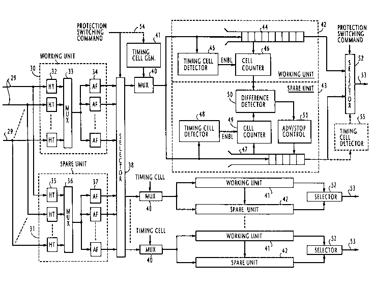
1 8 Referring now to Fig. 2, there is shown a duplicated ATM swit~hing
19 system incorporating the present invention in an output buffer (queuing)
20 arrangement. The output buffer ATM switching system includes an incoming
21 stage 30 of working unit and a duplicated, incoming stage 31 of spare unit
2 2 operating in what is called a "hot-standby" mode. Incoming stage 30 is made
2 3 up of a plurality of header translators 32 connected to receive incoming ATM24 cells from associated input ports 29. The outputs of header translators 32 are
25 time-division multiplexed in a multiplexer 33 and supplied through a TDM
26 (time division mul~iplex) bus to a bank of address filters 34 for extracting
27 ATM cells having the same address as the filters. Spare-unit incoming stage 31
28 is identically constructed to working-unit incoming stage 30 by header
29 translators 35, a multiplexer 36 and address filters 37.
3 o A selector 38 is provided for normally coupling the outputs of the

NE~82
CA~221 i
working unit address filters 34 respectively to multiplexers 40 and coupling the2 outputs of the spare unit address filters 37 to multiplexers 40 in response to a
3 protection switching command. A timing cell generator 41 periodically
4 supplies a timing cell to multiplexers 40 where it is multiplexed with an
5 incoming ATM cell stream. The output of each multiplexer 40 is connecte~ to
6 a set of working buffer unit 42 and spare buffer unit 43. The working buffer
7 unit 42 comprises a buffer 44 for buffering cells from multiplexer 40. A
8 timing cell detector 45 is provided for detecting a timing cell from the output
g of multiplexer 40. A cell counter 46 is connected to the buffer 44 to produce a
o signal representing the amount of cells remaining in the buffer. Spare buffer
11 unit 43 includes a buffer 47, a timing cell detector 48 and a cell counter 4912 which are arranged in a manner similar to the working unit 42, but additionally
13 includes a difference detector 50 and an advancelstop controller 51.
4 Cell counter 46 is enabled in response to the detection of a timing cell
5 by timing cell detector 45 for determining the number of cells stored in the
6 working output buffer 44, and cell counter 49 is enabled in response to the
detection of a timing cell by timing cell detector 48 for determining the
8 number of cells stored in the spare output buffer 47. Difference detector 50 is
19 connected between the outputs of cell counters 46 and 49 to produce a signal
20 reprt-sent~rive of the number of cells in the spare output buffer 47 which are
21 more or less than the number of cells in the working output buffer 44.
22 Advance/stop controller 51 is supplied with the output of the difference
23 detector 50 to provide an advance command to buffer 47 when the output of
24 cell counter 49 is greater than that of cell counter 46 or a stop command when
25 the output of cell counter 49 is smaller than that of cell counter 46.
26 The advance command causes buffer 47 to advance its read address
2 7 pointer by an amount corresponding to the number of cells by which amount
2 8 its cell count is greater than the cell count of buffer 44. The stop command29 causes buffer 47 to freeze its read address pointer for an interval corresponding
3 0 to the number of cells in buf~er 47 by which amount its cell count is smaller

-- NE~82
-6- CA2 ~ 6221 1
than the cell count of buffer 44. Similar read control operations proceed in
2 other working units 42 and spare units 43 in response to the same timing cell
3 produced by timing cell generator 41. Selector 52 responds to a protection
4 switching command pulse supplied from a maintenance center, not shown, by
5 coupling the spare output buffer 47, instead of the working output buffer 44,
6 to the associated output port 53. At the same time the selector 38 responds to7 the protection switching command pulse for coupling the outputs of spare
8 input stage 31 to multiplexers 40, instead of the outputs of the working input9 stage 30.
o It will be appreciated that, since the advance/stop control is performed
11 on the basis of the difference between the lengths of output queues in both
12 working and spare output buffers, the speed of the read timing adjustment is13 not required to be increased correspondingly to the operating speed of the
14 ATM swit~hing system.
In addition, the spare unit 43 is allowed a sufficient time to effect read
6 timing adjustment corresponding to the amount of cells in the working unit
42. As a result, the timing cell generator 41 may be triggered by the
8 protection switching command pulse to produce a single timing cell as
19 indicated by a dotted line 54 and a timing cell detector 55 is optionally
20 connecte~ to the output of spare buffer 47 to cause selector 52 to provide
21 protection switching in response to the detection of a timing cell, instead of to
22 the protection switching command pulse.
23 The present invention can be incorporated in a shared buffer ATM
24 switching system as shown in Fig. 3. The system includes a working input
stage 60 and a spare input stage 61. The working input stage 60 has a bank of
26 header translators 62 connected to input ports 59, and a multiplexer 63 for
27 combining the outputs of header translators 62 into a multiplexed ATM cell
28 stream onto a TDM bus 64, and the spare input stage 61 has a bank of header
29 translators 65 connected to input ports 59, and a multiplexer 66 for combining
the outputs of header translators 65 into a multiplexed ATM cell stream onto a

NE~82
~21 6221 1
--7 -
TDM bus 67. The TDM bus 64 is normally connected through a selector 68
2 to a multiplexer 69 where the multiplexed stream is combined with a timing
3 cell periodically produced by a timing cell generator 70.
4 A working unit 71 and a spare unit 72 are connected to the output of
5 multiplexer 69. Working unit 71 has a shared buffer memory 73, a timing cell
6 detector 74, a cell counter 75, a demultiplexer 76, and a routing and buffer
7 management (RBM) logic 77. The shared buffer memory 73 is a random-in-
8 random-out buffer. For each cell the RBM logic 77 analyzes the cell header
g and routes the cell to a logical buffer (queue) formed in the shared buffer
o memory 73 corresponding to an output port of the system. Shared buffer
memory 73 is controlled by the RBM logic 77 which is responsible for
12 controlling the free and occupied cell locations of the logical queue. Cell
13 counter 75 is connected to the shared buffer memory 73 to provide a cell
14 count value for each logical queue when enabled in response to the detection of
5 a timing cell by timing cell detector 74. Since a plurality of logical buffers are
16 formed in the memory 73, a timing cell is placed in each logical queue along
17 with ATM cells. The output of the shared buffer memory is connected to the
18 demultiplexer 76 where the cells from the memory are demultiplexed
19 according to their cell headers and supplied to selectors 84 which are
20 connected respectively to output ports 85.
21 Spare unit 72 has a shared buffer memory 78, a timing cell rletector 79,
22 a cell counter 80, a difference detector 81, a demultiplexer 82 and a RBM
23 logic 83 that provides routing and buffer management for each cell in the
24 shared buffer memory 78. Similar to cell counter 75, cell counter 80 provides
25 a cell count value of each logical queue in the shared buffer memory 78 when
26 enabled in response to the detection of a timing cell by timing cell ~letector 79.
27 Difference detector 81 is connected between the outputs of cell counters 75
2 8 and 80 to produce a plurality of difference signals each indicating the
2 9 difference between the cell count of each logical queue in memory 75 and the
3 0 cell count of a corresponding logical queue in memory 78. In response to the

- NEb82
-8- CA21 6221 1
difference signals, the RBM logic 83 controls the logical queues in memory 78
2 by advancing the read address pointer of each spare logical queue by an
3 amount corresponding to the number of cells in the spare logical queue by
4 which amount its cell count is greater than the cell count of the corresponding
5 working logical queue, or freezing the address pointer for an interval
6 corresponding to the number of cells in the spare logical queue by which
7 amount its cell count is less than the cell count of the corresponding working
8 logical queue.
g The output of the shared buffer memory 78 is decomposed into
1 o individual ATM cells by demultiplexer 82 according to their cell headers andl I supplied to all selectors 84, to which a protection switching command pulse is
12 applied as in the case of the output buffer ATM switching system. As an
13 option, the timing cell generator 70 is responsive to the protection swit~hing
14 command pulse for producing a timing cell and a timing cell detector 86 is
5 connected to the outputs of demultiplexer 82 to detect a timing cell and cause16 each selector 84 to provide protection switching.
17 If the amount of cells in the active buffer 44 is small, there is no
8 sufficient time to complete the advance/stop control of the spare buffer 47.
19 Under such circumstances it is desirable to suspend the advance/stop control
until the active buffer 44 is filled with a sufficient amount of cells.
21 To this end, the output buffer ATM switching system of Fig. 2 is
22 modified as shown in Fig. 4. In this modification, the spare unit 42 further2 3 includes a comparator 90 connected to the output of active cell counter 46 for
24 making a comparison with a predetermined threshold. Comparator 90
produces an output when the cell count of active buffer 43 is lower than the
26 threshold, the output being supplied to the advance/stop controller 51 and
27 selector 52 to disable their operation. In a similar manner, the shared buffer
28 ATM switching system of Fig. 3 is modified as shown in Fig. 5. A comparator
29 91 is provided in the spare unit 72 to compare the cell count of each logical
30 queue in the working shared buffer memory 73 with a threshold value and

- NE~82 CA21 6221 1
g
;
supplies a disable signal to the routing and buffer management logic 83 and to
2 a corresponding one of the selectors 84 when the cell count of that logical
3 queue is smaller than the threshold. The RBM logic 83 is thus prevented from
4 responding to a corresponding difference signal to suspend the advance and
s stop control of the corresponding logical buffer in the spare shared buffer
6 memory 78 as long as the cell count of the logical queue in that logical queue is
7 srn~ r than the threshold value.

Representative Drawing
A single figure which represents the drawing illustrating the invention.
Administrative Status

2024-08-01:As part of the Next Generation Patents (NGP) transition, the Canadian Patents Database (CPD) now contains a more detailed Event History, which replicates the Event Log of our new back-office solution.

Please note that "Inactive:" events refers to events no longer in use in our new back-office solution.

For a clearer understanding of the status of the application/patent presented on this page, the site Disclaimer , as well as the definitions for Patent , Event History , Maintenance Fee  and Payment History  should be consulted.

Event History

Description Date
Inactive: IPC expired 2013-01-01
Inactive: IPC from MCD 2006-03-12
Application Not Reinstated by Deadline 2000-09-07
Inactive: Dead - No reply to s.30(2) Rules requisition 2000-09-07
Deemed Abandoned - Failure to Respond to Maintenance Fee Notice 1999-11-08
Inactive: Abandoned - No reply to s.30(2) Rules requisition 1999-09-07
Inactive: S.30(2) Rules - Examiner requisition 1999-05-06
Inactive: Status info is complete as of Log entry date 1998-05-22
Inactive: Application prosecuted on TS as of Log entry date 1998-05-22
Application Published (Open to Public Inspection) 1996-05-05
All Requirements for Examination Determined Compliant 1995-11-06
Request for Examination Requirements Determined Compliant 1995-11-06

Abandonment History

Abandonment Date Reason Reinstatement Date
1999-11-08

Maintenance Fee

The last payment was received on 1998-10-21

Note : If the full payment has not been received on or before the date indicated, a further fee may be required which may be one of the following

  • the reinstatement fee;
  • the late payment fee; or
  • additional fee to reverse deemed expiry.

Please refer to the CIPO Patent Fees web page to see all current fee amounts.

Fee History

Fee Type Anniversary Year Due Date Paid Date
Request for examination - standard 1995-11-06
MF (application, 2nd anniv.) - standard 02 1997-11-06 1997-10-17
MF (application, 3rd anniv.) - standard 03 1998-11-06 1998-10-21
Owners on Record

Note: Records showing the ownership history in alphabetical order.

Current Owners on Record
NEC CORPORATION
Past Owners on Record
TAKATOSHI KURANO
Past Owners that do not appear in the "Owners on Record" listing will appear in other documentation within the application.
Documents

To view selected files, please enter reCAPTCHA code :


To view images, click a link in the Document Description column. To download the documents, select one or more checkboxes in the first column and then click the "Download Selected in PDF format (Zip Archive)" or the "Download Selected as Single PDF" button.

List of published and non-published patent-specific documents on the CPD .

If you have any difficulty accessing content, you can call the Client Service Centre at 1-866-997-1936 or send them an e-mail at CIPO Client Service Centre.


Document
Description 
Date
(yyyy-mm-dd) 
Number of pages   Size of Image (KB) 
Abstract 1996-03-25 1 26
Cover Page 1996-03-25 1 15
Description 1996-03-25 9 423
Claims 1996-03-25 9 370
Drawings 1996-03-25 5 133
Claims 1998-07-06 9 372
Description 1998-07-06 9 424
Abstract 1998-07-06 1 25
Drawings 1998-07-06 5 133
Representative drawing 1998-05-20 1 32
Reminder of maintenance fee due 1997-07-08 1 111
Courtesy - Abandonment Letter (Maintenance Fee) 1999-12-06 1 184
Courtesy - Abandonment Letter (R30(2)) 1999-11-02 1 171
Correspondence 1995-11-30 25 1,107