Note: Descriptions are shown in the official language in which they were submitted.
2 1 6294 1
METHOD AND APPARATUS TO CONTACT PLATING BAR
WITHOUT EXPOSING CONTACT COPPER OR REWORK OF THE
CONTACT PAD PLATING
Background
This invention relates to printed wiring boards in
general and more specifically to a method of plating
contact pads on printed wiring boards.
Printed wiring boards (PWBs), also known as printed
circuit boards, are widely used in the electronics industry
to connect together the various components of electronic
devices. A typical printed wiring board (PWB) may comprise
one or more layers of metal circuit paths or conductors
that are bonded onto an insulating substrate. The circuit
paths or conductors are co~mo~ly thin copper strips and the
insulating substrate typically comprises glass-reinforced
epoxy, although other materials may be used. Depending on
the complexity of the electronic circuit, PWBs may be
single sided, double sided, or may comprise multiple layers
of circuit paths or conductors, as in a multi-layer PWB.
Complex electronic circuits usually require the use of
double sided or multi-layer PWBs, which allow the printed
circuit paths to cross over each other without shorting and
without the need to add special jumpers. The materials
used for producing PWBs as well as PWB fabrication
processes are well-known and are documented in numerous
technical references such as, for example, Electronic
Materials Handbook, Volume 1-Packaging, (ASM International,
Materials Park, OH 44073, 1989), pp. 505-630, which is
hereby incorporated by reference.
While PWBs may be connected to one another and to
various other electrical components hy individual wires or
ribbon wire bundles that are soldered directly to the PWB,
it is usually more convenient to provide the PWB with a
plurality of contact pads positioned adjacent one or more
edges of the PWB. The contact pads are designed to align
with contacts in a suitable mating connector, thus allowing
the PWB to be connected to external circuitry or devices by
sim~lv insertinq the PWB into the mating connector. In
2 1 6294 1
order to ensure a reliable, low resistance electrical
connection, both the contact pads on the PWB and the
contacts within the mating connector are usually plated
with gold or a hard gold alloy. Gold, being a noble metal,
has excellent resistance to corrosion and maintains its low
contact resistance indefinitely.
An electroplating process is typically used to coat
the contact pads of the PWB with a suitable gold alloy.
However, since the electroplating process requires that an
electrical potential be placed between the object to be
plated and the electroplate solution, all of the contact
pads on the PWB must be electrically connected to the
appropriate voltage potential if they are to be plated.
A common method of electrically connecting together
the contact pads in preparation for plating is shown in
Figure 1. Essentially, a printed wiring board B includes
a circuit region C and a waste region W. The circuit
region C may include a plurality of contact pads P, as well
as a plurality of circuit paths or conductors (not shown)
that are required to connect together the various
electronic components (also not shown) that will later be
mounted on the board B. The waste region W may include a
plating tie bar or plating bar PB that is electrically
connected to the end E of each contact pad P by a thin
conductor strip or track T located on the surface of the
board B. A suitable voltage source (not shown) is then
connected to the plating bar PB to place each contact pad
P at the proper electrical potential required for
electroplating. After the plating process is complete, the
waste region W o~ board B is removed, usually by routing,
to expose a new edge L.
While the foregoing method for plating the contact
pads is widely used, it is not without its disadvantages.
For example, one disadvantage is that the underlying copper
conductors comprising the contact pads are exposed when the
waste region is removed by the router. Over time, the
Case No. 1094034-1
2 1 6294 1
exposed copper of the contact pads tends to oxidize, which
may compromise the integrity of the overlying gold plate.
In extreme cases, the oxidization of the underlying copper
may cause the overlying gold plate to flake away, which, of
course, significantly reduces the reliability of the
contact pad. Another disadvantage is that the router used
to separate the waste region from the circuit region may
also cause shorting between adjacent contact pads. More
specifically, the copper of the contact pad, being a
malleable material, may be drawn along the cutting path by
the router bit a sufficient distance so that it contacts
the exposed copper or gold plating of the adjacent contact
pad. The routing operation may also lift the copper
contact pad from the substrate, which, at best will cause
contact reliability problems and, at worst may ruin the
board.
An alternative method of connecting the contact pads
P to the plating tie bar PB is shown in Figure 2. In this
alternative method, all of the contact pads P are first
connected together by a plurality of lateral tracks T. The
contact pads P are then connected to the plating tie bar PB
by a single track S. While this method has been used, it
still suffers from all of the same problems as the method
shown in Figure 1. In addition, this method also suffers
from the disadvantage of requiring a secondary drilling
operation, after the plating operation, to cut the lateral
tracks T between adjacent contact pads P.
Consequently, there remains a need for a method for
connecting the contact pads to the plating bar that is not
subject to the disadvantages of current methods. Such a
method should result in a reliable contact pad and m;n;m; ze
the potential for the gold plate to flake off the pad or
otherwise become compromised. The improved method should
also be free from problems relating to removal of the waste
region, such as potential shorting between contact pads or
lifting of the contact pad from the board. Additional
Case No. 1094034-1
21 6294 1
advantages could be realized if the improved method could
be implemented in a conventional PWB fabrication process,
without requiring additional materials or process steps,
and certainly without the need to resort to secondary
drilling operations to break unwanted connections.
Summary of the Invention
Apparatus to contact a plating bar without requiring
the later exposure of the contact pad copper or rework of
the contact pad plating may comprise a printed wiring board
having a contact pad and a plating bar positioned in spaced
apart relation on the surface of the wiring board. An
electrically conductive track internal to the printed
wiring board has a first end positioned at about the
plating bar and a second end positioned at about the
contact pad. A first electrically conductive via extending
between the plating bar and the first end of the internal
track electrically connects the plating bar and the
internal track. A second electrically conductive via
extending between the contact pad and the second end of the
internal track electrically connects the internal track to
the contact pad.
A method of electrically connecting the contact pad
and the plating bar may comprise the steps of: Providing
an electrically conductive track internal to the printed
wiring board; providing a first electrically conductive via
between the plating bar and the first end of the internal
track; and providing a second electrically conductive via
between the contact pad and the second end of the internal
track.
A significant advantage associated with the internal
track and electrically conductive vias is that they allow
the waste portion of the board to be removed after the
plating process without exposing the underlying copper of
the contact pads. Consequently, the copper comprising the
contact pad is not prone to oxidization, with all its
Case No. 1094034-1
2162941
--5--
associated disadvantages. Another advantage is that since
the waste portion of the board can be removed without
contacting the ends of the contact pads, there is no chance
of lifting the contact pad from the board or creating
shorts between adjacent contact pads. Still another
advantage is that the internal tracks can be provided on
the appropriate internal layer at the same time the other
conductors are being laid down elsewhere on the internal
layer, thus dispensing with the need for additional process
steps. Similarly, the electrically conductive vias
connecting the internal tracks with the plating bar and
contact pads may be provided during the same process steps
required to provide other electrically conductive vias
between the conductors on the internal layer and the
conductors on the external surfaces the board.
Brief Description of the Drawinq
- Illustrative and presently preferred embodiments of
the invention are shown in the accompanying drawing in
which:
Figure 1 is a plan view of a portion of a printed
wiring board showing one arrangement for connecting the
contact pads to the plating tie bar;
Figure 2 is a plan view of a portion of a printed
wiring board showing another arrangement for connecting the
contact pads to the plating tie bar;
Figure 3 is a plan view of a portion of a printed
wiring board according to the present invention showing the
arrangement of the plating tie bar, contact pads,
electrically conductive internal tracks, and electrically
conductive vias;
Figure 4 is an enlarged perspective view of a portion
of the printed wiring board shown in Figure 3 more clearly
showing the arrangement of the electrically conductive
internal tracks, the contact pads, and the electrically
conductive vias;
Case No. 1094034-1
2162941
Figure 5 is a cross-sectional view in elevation of the
printed wiring board taken along the line 5-5 of Figure 3
showing the arrangement of the plating tie bar, contact
pad, electrically conductive internal track, and
electrically conductive thru-vias;
Figure 6 is a cross-sectional view in elevation of the
printed wiring board shown in Figure 5 after the waste
region has been removed; and
Figure 7 is a cross-sectional view in elevation of
another embodiment of a printed wiring board showing the
arrangement of the plating tie bar, contact pad,
electrically conductive internal track, and electrically
conductive blind vias.
Detailed Description of the Invention
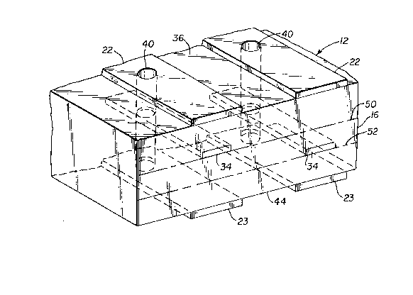
Apparatus 10 to contact a plating bar 18 without
requiring the later exposure of the contact pad copper or
rework of the contact pad plating is best seen in Figures
3 and 4 and may comprise a printed wiring board or PWB 12
having a circuit region 32 and a waste region 14. The
circuit region 32 of printed wiring board 12 includes a
plurality of contact pads 22 as well as a plurality of
circuit paths or conductors (not shown) required to connect
together the various electronic components (also not shown)
that will later be mounted on the PWB 12 and soldered to
the conductors to complete the electronic circuit. The
waste region 14 of PWB 12 comprises a plating tie bar or
plating bar 18 that will later serve as the connection
point for the voltage source (not shown) required to
accomplish electroplating of the contact pads 22. As will
be described in greater detail below, the waste region 14
later will be separated from the circuit region 32 along a
line 16, which then becomes the new edge of the printed
wiring board or PWB 12.
In order to electroplate the contact pads 22 with a
suitable material, such as gold or gold alloy, each contact
Case No. 1094034-1
2~6294~
pad 22 must be connected to the plating bar 18, which in
turn must be connected to a suitable electroplating voltage
source. In one preferred embodiment, each contact pad 22
is electrically connected to the plating bar 18 by an
electric conductor or track 34 that is internal to the PWB
12. However, since the plating bar 18 and the contact pads
22 are located on the external surface 36 of PWB 12, but
the tracks 34 are internal to the PWB 12, a pair of
electrically conductive vias 40 are used to connect each
internal track 34 to the plating bar 18 and to the contact
pad 22.
Once the all of the contact pads 22 have been
connected to the plating bar 18 by the internal tracks 34
and electrically conductive vias 40, the portion of the PWB
12 containing the contact pads 22 then may be submerged in
a suitable electroplating solution (not shown) containing,
for example, gold or a gold alloy. A suitable
electroplating voltage source (also not shown) may then be
connected to the plating tie bar 18, thus placing the
appropriate voltage potential between the contact pads 22
and the electroplating solution. After the plating
operation is complete, the PWB 12 may be removed from the
electroplating solution and the waste portion 14 of the PWB
12 removed, for example, by routing along line 16. Line 16
then becomes the new edge of the PWB 12. However, while
the new edge 16 is located near the ends 20 of the contact
pads 22, it does not contact the ends 20, thus leaving the
ends 20 of the pads 22 covered with a protective layer of
gold plate 42, as best seen in Figure 6.
A significant advantage of the present invention iS
that it prevents the ends 20 of the contact pads 22 from
being exposed after the waste portion 14 of the PWB 12 is
removed. Consequently, the copper comprising the contact
pad 22 is not prone to oxidization, with all its associated
disadvantages. Another advantage is that since the ends 20
of the contact pads 22 are not contacted by the router bit
~ N~ ln94n~4-l
2~62941
(not shown) during the routing operation, there is no
chance that the bit will drag along the edges 20 of the
contact pads 22, thus eliminating the possibility of
lifting the contact pad 22 from the board or creating
shorts between adjacent contact pads 22.
Still other advantages are associated with this
printed wiring board configuration. For example, in most
cases the printed wiring board 12 will comprise a multi-
layer printed wiring board with at least one internal
layer, although PWB 12 may comprise many internal layers.
In that case, the internal tracks 34 can be provided on the
appropriate internal layer at the same time the other
conductors are being laid down elsewhere on the internal
layer. Similarly, the electrically conductive vias 40
connecting the internal tracks 34 with the plating bar 18
and contact pads 22 may be provided during the same process
steps required to provide other electrically conductive
vias between the conductors on the internal layer and the
conductors on the external surfaces 36 of the PWB 12.
Consequently, the provision of the internal tracks 34 and
electrically conductive vias 40 may be accomplished without
the need for additional process steps. The present
invention also dispenses with the need for secondary
drilling operations to break any unwanted contacts between
the contact pads.
Referring now to Figures 3-6, the apparatus 10 to
contact a plating bar 18 without requiring the later
exposure of the contact copper or rework of the contact pad
plating will be described in detail. As mentioned above,
the printed wiring board (PWB) 12 may comprise a multi-
layer printed wiring board comprising one or more internal
layers 50, 52 of circuit paths or conductors, as best seen
in Figure 4. Such multi-layer printed wiring boards are
manufactured by first manufacturing a plurality of single
sided wiring boards (not shown) having the appropriate
routing of electrical conductors. Methods for fabricating
~ No. 1094034-1
2~ 6~94 1
single sided circuit boards are well-known in the art (see
for example Electronic Materials Handbook, Vol. 1-
Packaging, pp. 505-630). The various single side boaras
are then stacked, one on top of another, and pressed
together with a suitable bonding agent (not shown), thus
forming a single, unitary board with a plurality of layers
50, 52 (Figure 4) of internal circuit paths or conductors,
each of which corresponds to one of the individual wiring
boards (not shown). Methods for stacking and bonding of
single sided circuit boards to provide a multi-layer board
are also well-known in the art. The multi-layer printed
wiring boards 12 shown in Figures 3-7 comprise such
multiple layers of individual boards that have already been
stacked and bonded together, and are referred to herein in
the singular.
Referring now to Figure 3, printed wiring board 12
also comprises a circuit portion 32 and a waste portion 14.
The circuit region 32 of printed wiring board 12 includes
a plurality of contact pads 22, as well as a plurality of
circuit paths or conductors (not shown) required to connect
together the various electronic components (also not shown)
that will later be mounted on the PWB 12 and soldered to
the conductors to complete the electronic circuit. The
circuit region 32 of printed wiring board 12 may also
comprise additional contact pads 23 located on the opposed
or lower surface 44 of PWB 12, as best seen in Figures 4
and 5. The waste region 14 of PWB 12 comprises a plating
tie bar or plating bar 18 that will later serve as the
connection point for the voltage source (not shown)
required to accomplish electroplating of the contact pads
22, 23.
The plating bar 18 and contact pads 22, 23 are
electrically connected by a plurality of internal tracks 34
and electrically conductive vias 40. Methods for forming
electrical vias are well-known in the art. The internal
tracks 34 may be located on one or more of the internal
c r~ M~ 1 n q ~l n ~
2~629~1
-10--
layers 50 52 comprising PWB 12, as best seen in Figure 4.
Whether the internal tracks 34 are provided on any single
internal layer 50 or on several internal layers 50, 52
depends largely on the overall complexity of the circuit as
well as whether sufficient space is available on a given
layer for all of the tracks 34. Consequently, the present
invention should not be regarded as limited to any one
particular arrangement of internal tracks 34 on a single
layer 50 or on multiple layers 50, 52.
The electrically conductive internal tracks 34 may
comprise copper conductors and are aligned with the plating
bar 18 and the contact pads 22, 23, as best seen in Figures
4 and 5. It should be noted, however, that the material
comprising the conductors of the PWB, e.g., the
electrically conductive internal tracks 34, contact pads
22, and plating bar 18, is not limited to copper, and could
comprise any of a wide range of conductive materials, such
as aluminum, silver, gold, etc. However, copper is by far
the most commonly used material for PWB conductors. In one
preferred embodiment, the internal tracks 34 may be created
on the internal layers 50, 52 at the same time that the
other circuit paths or conductors are being laid down on
the internal layers 50, 52. After the internal layer 50 or
layers 50, 52 have been fabricated, they are then pressed
together with a suitable bonding material (not shown) in a
manner well-known in the art to form the single, unitary
PWB 12.
The electrically conductive vias 40 connecting the
internal tracks 34 to the plating bar 18 and the contact
pads 22, 23 are best seen in Figure 5 and may be provided
during the same process steps that are used to provide
other electrically conductive vias (not shown) required to
connect the circuit conductors on the internal layer 50 to
the circuit conductors on the upper and lower surfaces 36
and 44. In one preferred embodiment, the vias 40 may
comprise thru-vias that extend through the entire PWB 12,
r~.O No. 1()94034-1
21 ~29~ 1
as best seen in Figure 5. While many processes exist for
constructing such electrically conductive thru-vias, a
thru-via 40 may be constructed by drilling a hole through
the plating bar 18, one end 46 of internal track 34, and
all the way through the PWB 12 and an optional opposed
plating bar 19 on the lower surface 44 of PWB 12. Any one
of a number of plating processes may then be used to plate
the inside of the hole with a conductive material, thus
electrically connecting the internal track 34 with the
plating bars 18, 19. The electrically conductive thru-via
40 connecting the other end 46 of the internal track 34
with the contact pads 22, 23 may be constructed in a
similar manner.
After the electrically conductive vias 40 have been
constructed, the contact pads 22, 23 may be plated in a
conventional manner. For example, the contact pads 22, 23
may be immersed in a suitable electroplating solution (not
shown) and a voltage source (also not shown) connected
between the plating solution and the plating bar 18. After
the plating operation is complete, each contact pad 22, 23
will be encapsulated by a thin layer 42 of the plating
material, such as a gold alloy, as best seen in Figure 6.
The thin layer 42 also covers the ends 20, 21 of each
contact pad 22, 23 to prevent it from being oxidized by
exposure to the atmosphere. A suitable device, such as a
router (not shown) may then be used to remove the waste
region 14 of the PWB 12, exposing a new edge 16. The edge
16 may also be chamfered to remove sharp edges and prevent
splintering of the PWB 12. The ends 20, 21 of the contact
pads 22, 23 are not exposed by the routing operation, and
remain protected by the thin layer 42 of plating material.
Of course the contact pads 22, 23 on the upper and lower
surfaces 36 and 44 of the PWB 12 remain electrically
connected together by the thru-via 40, as best seen in
Figure 6.
Another embodiment 110 is shown in Figure 7 that uses
Case No. 1094034-1
216294~
a plurality of blind vias, 140, 141, which allow the
contact pads 122, 123 on the upper and lower surfaces 136
and 144 to remain electrically isolated. More
specifically, the embodiment 110 shown in Figure 7
comprises a pair of blind vias 140 to electrically connect
the plating bar 118 and contact pad 122 on the upper
surface 136 to an upper internal track 134 located on an
upper internal layer 150. Another pair of blind vias 141
are used to electrically connect a plating bar 119 and
contact pad 123 on the lower surface 144 to a lower
internal track 135 located on a lower internal layer 152.
The use of blind vias, such as vias 140 and 141, has the
advantage of allowing the contact pad 122 on the upper
surface 136 to remain electrically isolated from the
contact pad 123 on the lower surface 144, yet still be
connected to a plating bar 119 on the lower surface 144.
It is contemplated that the inventive concepts herein
described may be variously otherwise embodied and it is
intended that the appended claims be construed to include
alternative embodiments of the invention except insofar as
limited by the prior art.
Case No. 1094034-1