Note: Descriptions are shown in the official language in which they were submitted.
CA 02163395 2000-02-17
APPARATUS AND METHOD FOR SAMPLING SIGNALS SYNCHRONOUS WITH
ANALOG TO DIGITAL CONVERTER
BACKGROUND OF THE INVENTION
This invention discloses certain improvements to the
invention disclosed and claimed in U.S. Patent No. 5,315,527
issued to Robert W. Beckwith on May 24, 1994 (also the inventor
of the present invention) entitled "METHOD AND APPARATUS
PROVIDING HALF-CYCLE DIGITIZATION OF A-C SIGNALS BY AN ANALOG-
TO-DIGITAL CONVERTER"
Patent No. 5,315,527 discloses the digitization of
portions of an alternating current (AC) signal of selected
polarity for use where all
1
2163395
of the information necessary to make desired measurements of the entire
signal is contained in a selected portion of the signal. Patent No.
5,315,527 discloses certain inventive advantages in the use of a high
sampling rate in measuring the amplitude of an AC signal using a charge
coupled analog to digital converter (ADC). Patent No. 5,315,527 further
describes inventive ways of measuring the amplitude of at least two AC
signals and the phase angle between them. The measurement of the
average and the RMS value of amplitude are disclosed, as well as the
measurement of phase angle as the time between zero crossings of the AC
signals.
U. S. Patent No. 5,224,011 issued to Murty V. V. S. Yalla et al.
discloses an all-digital device for electric power system protective
relaying. In Patent No. 5,224,011, control voltage or current signals
are sampled by an ADC and the samples processed using Fourier Transforms
in order to extract factors required for computation essential to
performance of said device. These samples are taken at a rate
established by a multi-task operating system used by an associated
microprocessor.
U. S. Patent 4,419,619 issuedto James A. Jindrick et al., dated
December 6, 1983, (Jindrick) describes the use of microprocessor and
software modules for the control of a voltage regulating transformer.
Jindrick requires transforming digital voltage signals from the time
domain into the frequency domain to obtain a measured digital voltage
signal representative of the RMS voltage. In contrast to Jindrick, the
present invention computes the RMS amplitude of a signal directly in the
2
2163395
time domain and does not transform into the frequency domain. The
present invention also provides for the alternate computation of the
average amplitude of an input AC analog signal, or the computation of
the peak value of an input analog signal, all being computed directly in.
the time domain.
Furthermore, Jindrick requires processing a number of cycles to
obtain the RMS value whereas the present invention develops its full
measurement resolution on each half cycle sampled. Jindrick requires
the use of a software operating system whereas the inventive program
requires essentially no operating system. The MERTOS operating system
referenced by Jindrick may in itself be as large as the entire program
required by the present invention.
Another prior art signal sampling method is to synchronize a
specific number of samples with the power frequency thus fixing the
number of samples per cycle regardless of slow changes in the power
frequency. Such a method is described in an article by Gabriel Benmoual
entitled "AN ADAPTIVE SAMPLING-INTERVAL GENERATOR FOR DIGITAL RELAYING"
published in IEEE Transactions on Power Delivery, Vol. 4 No. 3 July
1989. In the present invention and in contrast to Benmoual, the
signal sampling rate is synchronized with a free running ADC in order to
more effectively utilize the sampling rate capability of said ADC.
Most of the foregoing methods require an analog anti-aliasing
filter in each AC signal channel ahead of the ADC for the purpose of
avoiding alaising or the incorrect assimilation or misinterpretation of
harmonic frequency components of said AC signal. The high sampling rate
3
2163395
of the present invention eliminates the necessity for anti-alaising
filters and, furthermore, improves the amplitude measurement accuracy of
a single AC signal cycle as will be described hereinafter.
Furthermore, much of the hardware, software and operating time in
equipment typified by the patents and articles listed above is used in
data processing and communications resulting in added cost and reduced
efficiency in the fundamental task of control or protection.
The present invention provides alternative communications having
higher data rates than usable over a telephone circuit, and passes the
data processing and communications work to a personal computer that is
only required when such data processing and communications are desired.
Only a very few percent of the inventive hardware, software and
operating time is used in serving this external computer.
Furthermore, controls and protective relays, as described above,
devote much hardware, software, and operating time in providing an
operator interface which may often be used for only brief periods in a
years time . Inventive ways of using said personal computer ( PC ) for the
operator interface are described hereinunder whereby said PC need only
be connected when required as an interface.
SUMMARY OF INVENTION
The present invention discloses inventive apparatus and methods for
4
2163395
using a microcontroller having a central processor unit ( CPU ) and an ADC
wherein a processor program is synchronized with the operation of the
ADC so as to maximize the rate of sampling of a plurality of AC input
signals.
The present invention also uses a linear program, herein defined as
one in which computational tasks are completed one at a time in contrast
to a multitask operating system wherein a number of tasks are scanned
with a set amount of time allocated to each task on each scan.
The present invention is illustrated using a microcontroller in
apparatus for the control or protective relaying of equipment for the
generation, transmission and distribution of electric power.
The present invention, is related to Patent No. 5,315,527 cited
above. The present invention discloses inventive methods and techniques
which may be combined to form various products. Inventive synchronous
and linear sub-programs run one at a time with an entry and an exit
point for easy linking in a modular manner to provide a complete
product. Apparatus using these inventive methods of programming is
termed herein as a "Synchronous Linear Machine" (SLIM). The inventive
methods enable program sub-routines of reduced size which are easily
linked together into a complete program: The inventive techniques
disclosed herein, result in products of high efficiency and low cost and
are improvements over prior art modular construction. Three examples of
such combination are given, one for a tapchanging transformer control,
one for a volts-per-hertz (E/Hz) protective relay and one for a single
phase differential current protective relay.
5
2163395
The present application also describes apparatus and methods for
reducing the frequency error caused by the finite period of the digital
samples in determining the actual zero crossings of the analog signals.
This error reduction is utilized herein for measuring the maximum E/Hz
of a three phase AC signal as well as for measuring frequency of an AC
signal.
Improved resolution and accuracy of voltage and current amplitude
and relative phase measurement are made possible by the high sampling
rate, as will be disclosed.
Non-synchronous computation and control subroutines, using the data
generated by the synchronous measurement subroutines are done linearly,
or one at a time, thereby simplifying the program structure and
minimizing the memory space required to contain the program. 11~a is
sent and received in short, high frequency bursts, to and from an
external personal computer (PC). This PC can also be used as a Network
Interface Module (NIM) to connect to a Local Area Network (LAN). The
data exchange with a NIM, the synchronous measurement subroutines, and
the linear computation and control subroutines may be combined, one
after the other, forming an overall program loop (See Fig. 6, for
example.) that cycles continuously until an operation, such as for
example a tapchange in a tapchanging transformer control, is called for.
No program interrupts are used other than on the time out of a watch dog
timer.
The PC is also used as the man-machine interface (MMI) for the
interconnected device which otherwise has a limited number of displays
6
CA 02163395 2001-09-28
such as LED's to indicate normal operal~ion. This reduces the
size of the operating program required for said device; and, in
addition, only a very small subroutine is required for the
device to send the communication bursts.
Therefore, in accordance with the present invention,
there is provided in an electronic device including a
microprocessor memory, an analog to d_Lgital converter (ADC)
having result registers and a central processor unit (CPU), the
method consisting of the steps of:
a) providing a CPU program consisting of steps and
loops,
b) operating said ADC and CPU synchronously,
c) continuously producing digital samples of analog
signals every "t" clock cycles,
d) storing said samples in said result registers,
e) updating at least one of said result registers
with new digital
samples every
"r" clock cycles,
and
f) reading said result registers integral multiples
of "r "' clock cycles after said result registers are updated,
wherein "r "' s not greater than "r" ,
i
g) providing an ADC controller having continuous
scan control bits, result register control bits, and input
channel select bits,
h) selecting analog signals by setting said input
channel select bits,
i) setting said continuous scan control bits to
obtain ADC conversions
in a continuous
round robin
fashion,
j) directing digital samples to selected ones of
said result
registers by
selection of
said result
register
control bits, for sampling a selected analog signal on integral
multiples of
"t" clock cycles,
7
CA 02163395 2001-09-28
k) adding do-nothing operations as required
to make the run time for each step and each loop of
said CPU program an integral multiple of "t" clock
cycles, and
1) obtaining sample's of said selected
analog signal by reading a selected result register
during said steps and said loops
thereby maximizing the sampling rate of the
selected analog signal and whereby said ADC and CPU
programs operate synchronously to obtain digital
samples of said analog signals.
Also in accordance with the present
invention, there is provided in an electronic device
including a central processor unit (CPU) operating at a
constant clock frequency, the method comprising the
steps of
a) providing a program for said CPU
consisting of program steps anal program loops each
operating in an integral multiple of a number of clock
cycles, "t",
b) summing said integral for each said step
and each turn of said loop starting said sum at a first
selected time and ending said sum at a second selected
time,
c) providing an analog to digital converter
(ADC) for converting AC signal: to digital samples,
said ADC having an analog to digital conversion time
equal to "t",
d) reading digital samples at a first AC
signal from said ADC with said program steps and said
program loops operating synchronously with analog to
7a
CA 02163395 2001-09-28
digital conversions of said ADC,
e) selecting a change in polarity of said
first AC signal as said starting time,
f) selecting the same change in polarity of
a later cycle of said first AC signal as the ending
point
whereby said sum is. a measure of the
frequency of said AC signal.
Further in accordance with the present
invention, there is provided an apparatus for
digitizing alternating current (AC) signals, each AC
signal coming from a first and second signal terminal
with the potential of said first terminal being the
ground reference for said signal and with the signal
potential of said second terminal alternating about
said reference potential comprising, in combination,
a) clocking means pro~;riding clock cycles,
b) analog-to-digital converter means (ADC)
operable by said clocking means a.nd having a conversion
period equal to a predetermined number "t" of clock
cycles, said ADC having at least one analog input,
having a low and a high reference voltage input and
having a range of operation starting with zero for an
analog input equal to said low reference input voltage,
c) processor means also operable by said
clocking means,
d) multiple result register means for
storing digital samples converted by said ADC,
e) said processor means running said ADC in
a continuously scanning mode with conversions of the
data of any selected analog input in a round robin
7b
CA 02163395 2001-09-28
fashion for storing in said multiple result registers
wherein digital samples of each said AC signal are
updated in integral numbers of clock cycles,
f) means for connecting a high ADC
reference voltage means to said high reference input,
g) each of said sE=_cond signal terminal
being connected to a selected ADC analog input
resulting in signals on said second terminals having a
selected polarity which is the same as the polarity of
said ADC high voltage reference,
h) said ADC having said low reference input
connected to a ground referencE: terminal to set the
change of signal polarity to said ADC zero,
i) said processor means containing
programming steps which selectively repeat with said
programming steps operating in integral multiples "m"
of said "t" clock cycles and ;paid programming steps
operating synchronously with said continuous scanning
mode of said ADC,
j) said ADC providing periodic non-zero
digital samples proportional to said AC signals
whenever the polarity of said AC signal is the same as
said high reference voltage and providing digital
samples which are zero whenever said AC signals are not
of the selected polarity, and
k) means for processing said non-zero
digital samples to make measurements to obtain
parameters of said AC signals.
Still further in accordance with the present
invention, there is provided an apparatus for
controlling and protecting electric power apparatus in
7c
CA 02163395 2001-09-28
response to measurement of volts per hertz in
alternating current (AC) signals,. three said AC signals
being of the same frequency and representing the three
phases voltages of a three phase circuit, comprising,
each signal coming from a pair of terminals with the
potential of one terminal being the ground reference
for said signal and with the signal potential of the
second terminal alternating about said reference
potential, said apparatus comprising in combination,
a) means for providing clock cycles,
b) a central proces:~ing unit (CPU) means
operable by said clock cycles,
c) an analog-to-dig_Ltal converter means
(ADC) operable by said clock cycles and having a
conversion period equal to a predetermined number "t"
of clock cycles, said ADC having at least one analog
input, having a low and a high reference voltage input
and having a range of operation starting with zero for
an analog input equal to said low reference input
voltage,
d) means for connecting said three AC
signals to said ADC means,
e) means for setting said ADC to perform
consecutive conversions on said three signals,
f) means for connecting a high ADC
reference voltage means to said high voltage reference
input,
g) means for connecting said ADC low
reference input to each said AC signal ground reference
terminal to set the change of signal polarity to ADC
zero,
'7 d
CA 02163395 2001-09-28
h) said processor means operating said ADC
in a continuously scanning mode to sequentially convert
a selected one of said three AC signals into digital
data and store said data in a round-robin fashion into
multiple result registers,
i) said processor means containing
programming means consisting of :steps which selectively
repeat and with said programming steps operating in
integral "m" multiples of "t" clock cycles to thereby
operate synchronously with the continuous scanning mode
of said ADC,
j) said ADC means p=roviding periodic non-
zero digital samples proportional to said selected AC
signals whenever the polarity of said selected AC
signal is the same as said high reference voltage and
providing digital samples which are zero whenever said
AC signal is not of the selected ~~olarity, and
k) said processor means receiving and
processing said digital samples to selectively
determine the maximum amplitude among the three phase
voltages, to enable determination of said AC signal
frequency and said volts per hez-tz from which desired
control and protection output signals may be obtained.
Still further in accordance with the present
invention, there is provided an apparatus for
measuring, controlling and protecting electric power
equipment in response to measurement of frequency
comprising, in combination,
a) means for digit_Lzing at least one
alternating current (AC) signal, each said signal
coming from a first and second terminal with the
7e
CA 02163395 2001-09-28
potential of said first terminal being the ground
reference for said signal and with the signal potential
of said second terminal alternating about said
reference potential,
b) a clocking means providing clocking
cycles,
c) an analog-to-digital converter means
(ADC) operable by said clocking means, having at least
one analog input, having a low and a high voltage
reference input and having a range of operation
starting with zero for an analog input equal to said
low reference input voltage,
d) a processor means operably responsive to
said clocking means,
e) multiple result register means for
storing conversions of said ADC,
f) said processor means operating said ADC
in a continuously scanning mode with conversions of the
data on any selected analog input in a round-robin
fashion for storing in said multiple result registers
wherein digital samples of AC signals are updated on
integral multiples of said conversion time of "t" clock
cycles,
g) means for providing a high ADC reference
voltage to said ADC high voltage reference input,
h) means for connecting at least one of
said second AC signal terminal to a selected ADC analog
input resulting in the signal's on said associated
second terminal having a selected polarity which is the
same as the polarity of said ADC high reference
voltage,
7f
CA 02163395 2001-09-28
i) said ADC means h<~ving said low voltage
reference input connected to each said AC signal ground
terminal to set a change of sign<~l polarity to said ADC
zero,
j) said processor containing programming
means consisting of steps which selectively repeat and
with said programming steps operating in integral
multiples of "t" clock cycles thereby forming a
programming which operates synchronously with said
continuous scanning mode of said .ADC,
k) said ADC means providing periodic non-
zero digital samples proportion<~1 to said AC signals
whenever the polarity of said AC signal is the same as
said high reference voltage and providing zeros
whenever said AC signal is not of the selected
polarity,
1) said processor means receiving and
processing said digital samples to determine the
approximate frequency from the time difference between
changes from zero to non-zero samples at the start of
two selected half cycles of said ;selected polarity,
m) means for determining the maximum
amplitude of each said selected half cycle, and
n) means for processing the first non-zero
sample of each said selected half cycle together with
said maximum amplitudes of said selected half cycle to
enhance the accuracy of the measurement of frequency of
said AC signal.
Still further in accordance with the present
invention, there is provided in an electronic device
including an analog to digital converter (ADC) and a
7g
CA 02163395 2001-09-28
central processor unit (CPU) having a common clock,
said ADC having result registers, ADC controller scan
control bits, result register control bits, and analog
channel select bits, the method comprising the steps
of
a) selecting analog ~~ignals by setting said
analog channel select bits,
b) setting said scan control bits to obtain
ADC conversions in a continuous round robin fashion,
c) taking digital samples from said ADC
using program loops operating in an integral "n"
multiple, together with program steps operating in an
integral "m" multiple, of the number of clock cycles
"t" required for an analog to digital conversion, and
d) summing said integral for each said step
and each turn of said loop starting said sum at a first
selected time and ending said sum at a second selected
time
whereby said sum becomes a measure of the
time interval from said starting time to said ending
time.
The foregoing features and advantages of the
present invention will be apparent from the following
more particular description of the invention. The
accompanying drawings, listed he;reinbelow, are useful
in explaining the invention.
DESCRIPTION OF THE DRAWINGS
FIG. 1 shows time lines useful to explain
synchronous programming.
7h
CA 02163395 2001-09-28
FIG. 2 shows time lines useful to explain
synchronous programming using a microcontroller such as
the Motorola MC68HC11 with program loops varying in
integral multiples of one tik in operating time.
FIGS . 3 (a) , (b) , and (c) show time lines
useful to explain synchronous programming using a
microcontroller such as the Motorola MC68HC16. FIG. 3d)
shows a block diagram of the ADC' system portion of the
HC16 microcontroller.
FIG. 4 is a circuit diagram showing signal
inputs to, and outputs from, a microcontroller as
useful in applying the inventive synchronous linear
machine to a tapchanger control.
FIG. 5 shows a load t:apchanging transformer
with tap switch, tap switch driving motor and motor
control together with a tapchange:r control.
7i
2163395
Fig. 6 is a flow chart for the SLIM measurement and control
program for a tapchanger control.
Fig. 7 is a flow chart of the SLIM measurement program used for a
tapchanger control.
Fig. 8 illustrates synchronous program diagrams for amplitude and
phase information using one voltage and two current signals as required
for a tapchanger control.
Fig. 9 shows a data readout system for providing a SLIM output to
a PC serving both as a MMI and as a NIM coupled to a second computer as
an entry point to a LAN.
Fig. 10 shows a data readout system for providing a SLIM output
through a personal computer to a remote facsimile unit via telephone
connections.
Fig. 11 is a circuit diagram showing signal inputs to an ADC as
useful in applying SLIM to a volts-per-hertz relay.
Fig. 12 is a flow chart for the SLIM measurement and control
program for a volts per hertz relay.
Fig. 13 is a flow chart of the SLIM measurement program used for a
volts per hertz relay.
Fig. 14 illustrates synchronous program diagrams for amplitude and
phase information using three phase voltages signals as required for a
volts per hertz relay.
Fig. 15 is a circuit diagram showing signal inputs to, and outputs
from, a microcontroller as useful in applying SLIM to a single phase
8
2163395
differential relay.
Fig. 16 is a flow chart for the SLIM measurement and control
program for a differential relay.
Fig. 17 is a flow chart of the SLIM measurement program used for a
differential relay.
Figs. 18-1, 18-2(a) and 18-2(b) show synchronous program diagrams
for a single phase differential relay.
DESCRIPTION OF INVENTION
DEFINITIONS OF VARIABLES
The following variables, as defined below, are used in the
specifications and claims:
t - ADC conversion time in clock cycles, (a tik)
Pt - ADC conversion time in seconds
r - clock cycles intervals between result register updates
r' - clock cycles a result register read lags a result register
update
x - the number of tiks a result is held in a result register
before being updated; note therefore that r = x * t
n - the length of a program loop in tiks
m - the length of a program step in tiks
CHOICE OF MICROCONTROLLER
Control and protective relay devices are used for control and
protection of equipment for generation, transmission and distribution of
electric power. These devices are used in various parts of the world
9
21b3395
and the devices must operate properly over a temperature range from -40
to +80 degrees celsius to assure proper operation under extreme
temperature conditions. Furthermore, said relay devices are subject to
high electric and magnetic disturbances. These may stem from lightning
strikes, from the opening of high voltage disconnect switches, and many
other sources of high energy, high frequency emanations. Also it is
traditional in the electric utility industry to expect long equipment
life of 20 years or more.
Microcontroller devices are now used in control and protective
circuitry in electric utility applications. In view of the demanding
requirements of such utility applications it is desirable to use a
microcontroller using level sensitive ( static ) logic as compared to edge
triggered logic. The microcontroller may, therefore operate at
relatively low clock speeds. The microcontroller should be transient
protected at all inputs and outputs and relatively insensitive to
misoperation due to all forms of electromagnetic radiation from 60 hertz
up to cosmic rays.
The microcontroller 1 as shown in Figs. 4, 11, and 15, utilized in
preferred embodiments of the invention, is a Motorola MC68HC11E9 (HC11)
which is a single chip device and which is readily available at present;
however, other microcontrollers with similar characteristics could be
used in the present invention and the invention is not limited to the
use of a specific microcontroller. References to the HC11 relate to the
68HC11 as described in Motorola HCII REFERENCE MANUAL M68HC11RM/AD REV
1,1990. The HC11 is available with 12K of EPROM 4, used for storage of
2163395
programs described herein, has 512 bytes of RAM 5, used by the CPU 7 for
scratch pad memory, and 512 bytes of EEPROM 6, used as non-volatile
storage of setpoints and other data which must be maintained upon loss
of power. The HC11 has a system clock frequency of 2 mhz, or less,
operated by oscillator 8 using crystal 14 operating at four times the
system clock frequency. The HC11 also includes an ADC 2 which is
connected and configured to operate from the same system clock from
oscillator 8 as the CPU 7 to provide the inventive synchronous
operation.
As stated above, the number of clock cycles "t~~ for any ADC to make
a conversion is hereinafter called a "tik". In some microcontrollers
"t" is fixed, in others, "t" is settable.
Referring to Fig. 4, in the microcontroller 1, the ADC 2 performs
an analog to digital conversion in one tik, -with the result being
transferred into the result registers 11 in a part of the clock cycle.
The results in the registers are read at times when results are not
being entered, therefore no interference occurs between reads and result
updates.
As alluded to above, the present invention may also utilize other
controllers with a more flexible ADC control matrix such as a Motorola
MC68HC16 microcontroller. Reference herein to the HC16 relates to the
MC68HC16Z2 as described in Motorola M68HC16 USERS MANUAL
MC68HC16Z2UM/AD. The Motorola MC68HC16 microcontroller (HC16) is a 16
bit device which is of the same family as the HC11 microcontroller. The
HC16 microcontroller has a very flexible ADC control matrix shown as the
11
CA 02163395 2000-02-17
Mode and Timing Control of FIG. 3d), which permits a program to
set the ADC conversion period to any predetermined number of
clock cycles from 16 to 32 and also permits coupling up 8 analog
inputs to 8 output registers for continuous scanning in a choice
of 8 or 10 bit resolution. It is possible to set the ADC control
in a program independent manner and accommodate a wide variety
of synchronous programs using the inventive means and methods,
including the possibility of scanning some inputs more often
than others. In general, any result register 0 . . . 7 of FIG.
3d) can be set so as to be updated at integral multiples of said
predetermined conversion period.
FIG. 3(a) illustrates use of the ADC 20 of an HC16.
FIG. 3(d) depicts the ADC 20 portion programmed to digitize 8
inputs, ANO through AN7, associated with registers 21 labeled RO
through R7 and using a program loop from 16 to 32 clock cycles
long. In ADC 20 the sampling time can be set from 16 to 32 clock
cycles permitting the program loop to be written as short as
possible (down to 16 clock cycles). The ADC 20 can then, in
general, be set to match the number of clock cycles in a program
rather than requiring the program loop to be written with do-
nothing cycles to match the ADC 2, as with the HC11; as will be
described hereinafter. FIG. 3(b) illustrates a program loop two
tiks long, and FIG. 3(c) illustrates a program loop three tiks
long.
As will become apparent, the inventive apparatus and
methods are equally applicable to microcontrollers having
generally similar capabilities as the HC11 or HC16.
12
21~33~~
SYNCHRONOUS PROGRAMMING -
Referring again to Fig. 4, the present invention discloses an
apparatus including a microcontroller 1 operating selectively in a
synchronous mode and a linear mode, and methods of selectively
utilizing the apparatus in synchronous modes and in linear modes. The
ADC 2 has an associated control register (ADCTL) 12 having scan control
bits, result register control bits and input channel select bits. AC
signals connected to the ADC 2 are sampled by the ADC 2 running in a
continuous sampling mode as set, using said scan control bits. A
program then runs bit synchronous with said ADC 2 thus minimizing the
need for ongoing program commands from the program to said ADC 2.
Figs. 1, 2 and 3 illustrate the programming techniques required to
achieve synchronous operation using an HCll. While, in general, ADC's
inputs may be sampled at any integral "x" multiple of their analog to
digital conversion time, in the HC11 there is a choice for the integer
between one or four. The HC11 has a predetermined conversion period "t"
fixed at 32 clock cycles and has a relatively restricted set of
instructions for ADC 2 which permit two alternative modes of operation
of ADC 2. A first alternative mode (A) of operating ADC 2, is obtained
by setting said result register control bits for continuous sampling of
an input channel selected by said input channel select bits and with
results being stored, round robin fashion, in four result registers,
R1. . . R4 . "Round robin" as referred to in the Motorola reference manual
is best shown in Fig. 1 ( f ) , where a succession of program steps, P1
through P8 read result registers 11 in the repeating fashion of Fig.
13
CA 02163395 2000-02-17
(e). The second alternative mode (B) of operating the ADC 2 is
obtained by setting said result register control bits to
selectively sample either the first four or the second four
input channels, said selection obtained by setting of the input
channel select bits, such as to sample said four analog input
signals, in round robin fashion, with results being stored in
four corresponding result registers, R1 . . . R4.
For synchronous operation, and as mentioned above, in
the present invention the ADC 2 is connected and configured to
operate from the same system clock as CPU 7.
The upper limit of the HC11 frequency, and the
frequency used in the following explanations, is provided by
oscillator 8 at 8 Mhz as established by crystal 14, but since a
4 phase clock is used, the clock rate has an upper limit of 2
Mhz. The CPU 7 program uses only one of the oscillator 8 phases,
and the ADC 2 updates the result registers on the other phases .
The ADC 2 updating of one of the result register 11 and program
reading of a register thus cannot interfere with each other.
The synchronous measurement methods of the invention
will now be described. In general, the method provides for
reading result register 11 samples every selected integral
number "m" tiks. The methods can best be explained with three
time vectors as shown in FIG. 1. The first is the pointer "T"
which is real time. A second time pointer, "U", describes the
updating of result registers, R1, R2, R3, and R4 by a free
running ADC 2. The third time vector "P" represents the time at
which the synchronous program reads the result registers 11.
Vector P lags
14
216335
the registers 11 update by a time which may be determined by chance when
the synchronous program starts. The lag time "r "', in clock cycles
remains constant until the synchronous program ends.
Note that Fig. 1 is a one dimensional display of time lines in the
horizontal direction with time events within boxes or indicated by
pointers. Fig. 1(a) depicts an ADC 2 result register R1 updated at a
time Ul and held for a time period represented by the box labeled Rl;
Fig. 1(b) shows register R2 updated at time U2, one tik after register
R1. Figure 1(c) illustrates an ADC 2 result register R3 updated at time
U3, two tiks after register R1; and Fig. 1(d) illustrates an ADC 2
result register R4 updated at time U4, three tiks after register R1.
With the ADC 2 configured for free running, Figs. (a), (b), (c), and (d)
each depict the respective registers R1, R2, R3, R4 holding a result for
four tiks after which they are again updated.
In Fig. 1(e), Figs. 1 (a), (b), (c), and (d) are combined with the
register time periods superposed on a single time line with only the
first tik from Figs.l (a), (b), (c), or (d) being indicated.
In Fig. 1(f), assuming use of the HCll, the program running time
vectors, shown as arrowed lines, P1, P2,....P8 show the times of reading
of the respective registers by a program loop set to take exactly 32
clock cycles per turn of the program loop. Program loops PLl, PL3 and
PL5 of Fig. 7 are typical 32 clock'cycle loops with Fig. 7 illustrating
their use to detect zero crossings of an alternating current (AC) signal
and entering the results in respective result registers as will be
described more fully hereinbelow.
2163395
The program time pointers or arrows P1. . . P8 of Figure 1 ( f ) , may be
moved forward or backward to any clock cycle whatsoever with the only
difference being the time the program data reads lag behind real time.
In other words, the registers R1, R2, R3, and R4 hold the data 4 times
32 = 128 clock cycles and the program data may lag behind real time from
one to 128 clock cycles depending on when the program happens to start
with relation to the ADC 2 cycle of register updating. The synchronous
program can start on any one of the 32 clock cycles within any tik and
thereafter will not deviate from that particular clock cycle within
subsequent tiks until the synchronous sub program is completed.
Note also that the program may start with any register. Fig. 1(g)
depicts an example of starting with register R4. In the structure
depicted in Fig. 1 the registers R1, R2, R3, and R4 contain samples from
one analog input in accordance with a first mode of operating the ADC 2.
However, as stated above, the ADC 2 is also operable by storing four
signals in corresponding registers.
Depending on the task required for a synchronous program step or
program loop, it may be necessary for the program step or program loop
time to be greater than one tik. This invention provides program steps
or program loops of varying integral number "m" or "n" , respectively, of
tiks in operating time as described below so that they will each run
synchronously with the ADC 2. Thus a synchronous program step or
program loop must have all operations whose operating time is data
independent and, if necessary, include fixed time do-nothing steps to
round off the operating time to an integral multiple of tiks.
16
2163395
Fig. 2, continuing to assume use of the HC11, illustrates
synchronous programming with several combinations of program loops from
one to four tiks in length and using both modes of ADC 2. As stated
above, one embodiment of the present invention provides a program that
samples registers during each program loop with the loop operating in 32
clock cycles, or one tik, thus obtaining data from each result register
R1, R2, R3, R4 in the order 1, 2, 3, 4, 1, 2, ...etc. as depicted by
Fig. 2(a). The use of ADC 2 in said first mode provides a sampling rate
of one sample per tik. Fig. 2(a) depicts an ADC 2 time vector U updating
result registers R1, R2, R3, and R4 in round robin fashion at times U1,
U2, ...UN. A synchronous program vector P is depicted in Fig. 2(a) for
a program loop one tik long. Vector P illustrates a program loop one
tik long sampling the result registers R1, R2, R3, and R4 in round robin
fashion at times P1, P2, ...Pn. The sampling will occur at some clock
cycle of the program loop at the programmers choice, it making no
difference which one. This synchronous feature reduces the program
complexity, permitting useful program loops to be only one or two tiks
in length, and in turn this increases the frequency of sampling. Thus
the inventive apparatus and methods of the invention achieve the high
sampling rate that is required to achieve the averaging of ADC 2 errors
disclosed by the previously mentioned Patent 5,315,527
As also depicted by Fig. 2 (a), if said second mode of operation of
the ADC 2 is selected and thereby four signal channels are assigned, one
to each register, each input is sampled every four tiks with the program
reading the result registers in the order R1, R2, R3, R4, R1,...etc
17
the reg
2163395
Fig. 2(b) depicts the use of a program with a length of 2 tiks.
Using the first mode of operating ADC 2, a single signal is scanned into
all four registers, and the program alternates in reading registers R2
and R4 to pick up every other signal sample; that is, one every two
tiks. Alternatively registers R1 and R3 could be read cyclicly with the
same result.
Fig. 2(c) depicts the order of sampling of the registers 11 for a
program loop length of three tiks. Fig. 2(c) illustrates the use of the
first mode of ADC 2 providing a single input to all four result
registers R1, R2, R3, R4 with a sample every three tiks. Fig. 2(c) also
depicts the use of the second ADC 2 mode providing four signal inputs to
four corresponding result registers R1, R2, R3, R4, with each input
being sampled every twelve tiks. ~~
Fig. 2 ( d) , continuing to assume use of the HC11, depicts the order
of reading of the registers for a program loop length of four tiks.
When the first mode A of ADC 2 is used and a sample of a single signal
every four tiks is provided, the program reads one of result registers
R1, R2, R3, or R4, the choice being arbitrary. The arrows marked U1,
U4, U7, U10, U13 show the ADC updating result register R1 every four
tiks. The arrows marked P1, P4, P7, P10, P13 shows said four tik
program loop taking samples of result register R1 every four tiks, just
after the updates by the ADC. It is clear from Fig. 2(d) that any of
the four result registers R1, R2, R3, or R4 could have been chosen and
that the lag time "r"' could be any one of 128 clock cycles during which
the contents of the chosen result register remains unchanged.
18
2163395
When the second mode B of ADC 2 is used and samples of four signal
inputs to four corresponding registers R1, R2, R3, R4 are provided, said
four bit program loop reads, in round robin order, R1, R2, R3, R4,
obtaining a sample of each signal input every sixteen tiks.
For using of this inventive method using an HC11 with from five to
eight ADC 2 inputs, mode B is used with the result register control
bits set to input the first four ADC 2 analog inputs. After the first
four ADC 2 inputs have been read by the synchronous program, the program
switches the result register control bits to input the second four
analog inputs. The program then continues to alternate between the first
four and the last four ADC 2 analog inputs.
APPLICATION PROGRAM LIBRARIES
Communications, computations and controls using the synchronously
measured data generated by the ADC 2 of HC11 are done linearly, that is,
one at a time, thereby simplifying the program structure and minimizing
the memory space required to contain the program. In one form of the
invention, the linear sub-programs are written to run in a data
independent fixed number of clock cycles. This enables the calculation
of the run time df a one program loop consisting of synchronous
measurement, linear computation and control and communications. As this
loop is used for control or protective relay purposes, an operations
timer is updated, thus the program run time becomes the timer without
the use of program interrupts. Alternative methods of measuring time,
for example using timers on board the MCU may be used.
Controls and protective relays used for electric utilities
19
CA 02163395 2001-09-28
generally require one or more voltage and current
measurements and since there is a limited number of
ways to make these measurements, a library of
synchronous measurement subroutines is formed. These
measurement subroutines as well as other linear
computations address only one task at a time and have a
single entry point and a single or at most a limited
number of branching exit points. Once a library of such
sub-routines is formed, the modular linkage into
programs for various devices may be obtained.
The inventive principles of synchronous
measurement and linear programming are further
clarified in the following examples of their
application.
APPLICATION AS A TAPCHANGER CONTROL
An analog type of t:apchanger control is
described in U.S. Patent No. 3,721,894 issued to R. W.
Beckwith, the inventor hereof. Inventive programming
methods are illustrated hereinafter permitting
replacement of said analog type of tapchanger with an
improved digital form using the inventive concepts.
A digital tapchanger control has also been
described by Murty V. V. S. Yalla et al. in U.S. Patent
No. 5,581,173, which issued on December 3, 1996.
In this example, the positive half cycles of
AC voltage signal E
20
2163395
and AC current signals I1 and I2 are digitized and the negative half
cycles suppressed to zero as described in detail in Patent No. 5,315,527
referenced above.
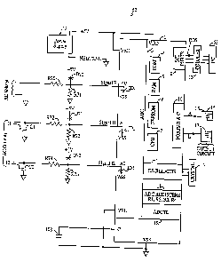
Fig. 4 is a circuit diagram of a tapchanger control showing signal
inputs E, I1 and I2 to an ADC 2 of microcontroller 1 of the tapchanger
control 62. Tapchanger control 62 is also shown in Figs. 5, 9 and 10.
One input is an AC voltage with a nominal voltage of 120 volts and with
an upper limit of 140 volts. Resistors R70 and R71 scale said upper
limit voltage, producing a signal E connected to ADC 2 input A0, so that
the peak of signal E will not saturate the ADC 2. A second input is
current I1 which produces a voltage across burden capacitor C1, which
voltage is scaled by resistors R72 and R73 producing signal I1 connected
to ADC 2 input A1, so that the peak of signal I1 will not saturate the
ADC 2 with in a linear range required for current I1. A third input is
current I2 which produces a voltage across burden capacitor C2, which
voltage is scaled by resistors R74 and R75 producing signal I2 connected
to ADC 2 input A2, so that the peak of signal I2 will not saturate the
ADC 2 within a linear range required for current I2. Protective diodes
D7O, D71, and D72 limit the positive excursion of voltage into the ADC
2 inputs while the. protective diodes ID1 contained in an HC11 protect
the ADC 2 inputs from negative excursion of signal voltages. The signal
current into all said protective diodes is safely limited by resistors
R70, R72, and R74. The ADC 2 high voltage reference, VRH, is connected
to +5 volts do and the ADC 2 low voltage reference, VRL, is connected to
ground. A conventional power supply 18 supplies 5 volts do to
21
2163395
microcontroller 1.
Fig. 5 shows a load tapchanging transformer 100 having a primary
winding 101 and a tapped secondary winding 102. A tapchanging motor
power supply transformer 103 has a primary 116 connected to the
regulated voltage produced by the tapchanging operation iri selecting
taps 113. The secondary 117 drives the tapchanging motor M via winding
W. Said winding W has a 'raise portion 114 and a 'lower' portion 115.
Transformer 106 produces a nominal 120 Vac sensing voltage for
tapchanger control 62 and current transformer 107 senses transformer 100
load current for tapchanger control 62. When the tapchanger control 62
operations timer LC (note sub-program 42 of Fig. 6) times out, the
tapchanger control closes either a 'raise' contact R (16) or a 'lower'
contact L (17), operating motor starter RR, raise, or RL, lower. Said
starter RR and RL cause motor run contacts 109 and 110 respectively to
close, causing the tapchanger motor to run in the indicated direction
and driving tapchanger switch 104 to effect either an increase (raise)
or decrease (lower) of the tap position 113. The tapchanging operating
mechanism 105 may take from, say 0.4 seconds to 4.0 seconds to make the
tapchange, depending on the particular switch characteristic. Counter
contact 108 included in motor drive mechanism 105 closes momentarily
indicating that said tapswitch 104 change is complete. Contact 111 is
a part of motor starter RR and closes indicating that a 'raise' is being
performed by motor M. Likewise contact 112 closes to indicate that a
'lower' is being performed by motor M. These contacts respectively
provide inputs RR and LR to tapchanger control 62.
22
2163395
Tapchanger control 62 is an example of a synchronous linear machine
(SLIM) and is further included in Figs. 9 and 10 illustrating
communications connections to a SLIM.
SYNCHRONOUS MEASUREMENT SUB-PROGRAM
Fig. 6 illustrates an overall program flow diagram for a tap-
changer control 62. The synchronous measurement sub-program (SM) flow
diagram is as described in Fig. 7. While this sub-program is running,
all other operations are blocked and interrupts are not used except in
the watchdog timer, not shown, which is continuously reset by a properly
running program. The SM sub-program ordinarily has but one entry and
one exit point.
Fig. 8 (a) illustrates the synchronous measurement of the amplitude
of a voltage E by program loop PL2 shown on Fig 7. Fig. 8 (b)
illustrates synchronous measurement of the amplitude of a current I1 by
program loop PL4 shown on Fig. 7. Fig. 8 (c) illustrates synchronous
measurement of the amplitude of a current I2 by program loop PL6 shown
on Fig. 7. Fig. 8 also illustrates measurement of the phase angles
between voltage E and currents Il and I2 using zero crossing detecting
program loops PL1, PL3, and PL5. Program loops PL1, PL3, and PLS, each
one tik long, and amplitude measuring program loops PL2, PL4, and PL6 of
Fig. 7, each two tiks long are linked together by program steps PS1,
PS2, PS3, PS4, and PSS, each one tik long. Figs. 7 and 8 together show
entry into the synchronous measurement program by program step PSO and
the sequential operation of. the program in the order PL1, PS1, PL2, PS2,
PL3, PS3, PL4, PS4, PL5, PS5, PL6, and finally the exit by program step
23
2163395
PS6.
Each dot on the axes of Figs. 8 (a), (b), and (c) represent the
taking of digital samples whose value is zero and each vertical line
under the positive signal half cycles of Figs. 8(a), (b), and (c)
represent the taking of digital samples whose values are non-zero. On
Fig 8, horizontal and vertical arrowed lines, starting with PSO,
continuing with PL1, PS1, PL2, PS2, PL3, PS3, PL4, PS4, PLS, PS5, PL6,
and ending with PS6 illustrate a synchronous measurement sampling path.
The ADC 2 control logic is set to sample an AC signal E every tik,
and enter the results in a round robin fashion into the result registers
R1, R2, R3, R4, R1, etc. as depicted by Fig. 1.
In Fig. 8, program loops PL1, PL3 and PLS, each one tik long, scan
the result registers R1, R2, R3, R4, R1, etc. as depicted by Fig. 1,
looking for transitions from a reading of zero to a non-zero reading
(znz) and exiting when said transition is found. Measurement program
loops, PL2, PL4 and PL6 each two tiks long, make a partial computation
for the amplitude measurement of one half cycle of an AC signal,
operating in time sequence as depicted by Fig. 2 (b), and exiting when
a non-zero to zero (nzz) transition is found.
There are various methods for obtaining amplitude measurements; two
useful known methods are:
A. Take the square root of the sum of the squares of the samples
(rms), wherein measurement program loops such as PL2 of Fig. 7 computes
the sum of the squares.
B. Take the average of the samples where a measurement program
24
CA 02163395 2000-02-17
loop computes the sum of the samples having the advantage of
shortening said measurement program loop to one tik per turn.
An additional inventive method is described
hereinbelow:
C. Take a filtered peak value (Ep) as the maximum of
Ep from the recursive equation:
Ep=((D*Ep)+Es)/(D+1); during one half wave measurement
of an AC signal, E,
Where Es is each sample, and where D is found by
multiplying the count of the number of samples in a previous
half wave of the AC signal E by a constant K, and rounding the
result to the nearest integer. K is chosen to be less than one
so as to select a number of samples less than the total number
of samples in a half wave of the AC signal. Note that "*" is
used in equations herein to denote multiplication.
In this way, the choice of K determines the portion of
a half cycle used in determining the peak amplitude of the wave
regardless of the frequency of the AC signal.
Method A, listed above is used for the tapchanger
control described further hereinbelow. Method B may be
advantageous where the method permits a one tik measurement
program loop thus improving the phase angle resolution. Method C
is advantageous for volts per hertz measurements to be described
hereinafter.
The following is a detailed description of the
synchronous operation of the sub-program diagrammed in FIG. 7.
FIG. 7 illustrates an unique real time flow diagram depicting
the time sequence of programming events; however, the horizontal
axis is a time sequence, but
2163395
is not a linear time scale. Program loops PL2, PL4, and PL6 are shown
twice as large as program loops PL1, PL3, and PL5 to illustrate the fact
that the former three program loops are each two tiks long and the
latter three program loops are each one tik long. Each of the program
steps PSO through PS6 is one tik long.
Figs. 8 (a), (b) and (c) show the portions of ADC 2 input signals
E voltage, I1 current, and I2 current which fall within the active
dynamic range of the ADC 2 as discussed in U. S. Patent No. 5,315,527
referenced above: In contrast to Fig. 7, the horizontal axes of Figs.
8 (a), (b), and (c) are coordinated real time scales. Since one tik is
so small on the time scale used, PS1, PS3 and PS5 appear as angled
double brackets, » . Program step PSO, which is the exit statement
of a previous sub-program and the entrance statement for the subsequent
synchronous sub-program, performs the following:
1) Switches AC voltage E into the ADC 2. (See Fig. 8(a)),
2) Starts program loop PL1. (See Fig. 7),
Program loop PL1 performs the following:
1) Takes samples of result registers R1, R2, R3, R4, (Shown in
Fig. 1) in round. robin fashion. As stated above, it is immaterial which
register is read first,
2) Looks for zero samples of signal E,
3 ) After finding non-zero samples, looks for a non-zero sample of
signal E, and
4) Exits to PS1 after the first non-zero sample of signal E is
obtained.
26
2 ~ 63395
Program step PS1 performs the following:
1) Sets a sum SS1 to zero,
2) Computes the square of the first sample of signal E and adds
to the sum SS1 thus forming the sum of squares SS1 in accordance with
method A above. At this point, one of the other alternative methods of
determining the amplitude of the AC signal mentioned above could be used
in lieu of the sum of squares method.
3) Records the number of the result register (R1, R2, R3, or R4)
from which the first non-zero sample of signal E was taken,
4) Sets a count of tiks to zero, and
5) Exits to PL2.
Program loop PL2 performs the following:
1) Takes a sample of every other one of registers R1, R2, R3,
R4, in round robin fashion as if PL2 had taken the first non-zero
sample. For instance, if the register recorded under program step PS1
3) was R1, then this program loop samples: R3, R1, R3, Rl...etc. If the
first register sampled was R4, then this program loop samples: R2, R4,
R2,...etc.
2 ) Continues the summing of the squares SS1 of the samples of
signal E,
3) Counts the number of samples of signal E,
4) Looks for a sample of signal E with the value zero, and when
zero is sensed,
5) Updates the count of tiks with each turn of said loop, and
6) Exits to PS2.
27
2163395
Program step PS2 performs the following:
1) Records count of tiks as t1 and updates count of tiks,
2) Stores the sum of the squares SS1 of the samples of signal E,
3) Stores the count of the number~of samples taken during PL2,
4) Switches current I1 signal to the ADC 2, and
5) Exits to PL3
Program loop PL3 performs the following:
1) Takes samples of result registers R1, R2, R3, R4, in round
robin fashion,
2) Looks for zero samples of signal I1,
3) After finding zero samples, looks for a non-zero sample of
signal I1,
4) Records the number of samples of signal I1 taken,
5) Updates the count of tiks with each turn of said loop, and
6) Exits to PS3 after the first non-zero sample of signal I1 is
obtained or when the number of zero samples exceeds the expected number
of samples for a complete cycle of signal I1, indicating that the
amplitude of current I1 is zero.
Program step PS3 performs the following:
1) Records count of tiks as t2 and updates count of tiks,
2) Sets sum SS2 to zero,
3) Computes the square of the first non-zero sample of signal I1
and adds to the sum SS2 in accordance with method A above. At this
point, one of the other alternative methods of determining the amplitude
of the AC signal mentioned above could be used in lieu of the sum of
28
2163395
squares method,
4) Records the number of the result register R1, R2, R3, or R4
corresponding to the register from which said first non-zero sample was
taken, and
5) Exits to PL4
Program loop PL4 performs the following:
1) Takes a sample of every other one of registers R1, R2, R3, R4,
in round robin fashion, as if PL4 had taken the first non-zero sample.
For instance, if the register recorded under program step PS3 3) was R1,
then this program loop samples: R3, R1, R3, Rl...etc. If the first
register sampled was R4, then this program loop samples: R2, R4,
R2,...etc.
2) Continues obtaining the sum of the squares SS2 of the samples
of signal I1,
3) Counts the number of samples of signal I1,
4) Looks for a sample of signal I1 with the value zero, and when
zero is sensed,
5) Updates the count of tiks with each turn of said loop, and
6) Exits to PS4.
Program step PS4 performs the following:
1) Records the count of tiks as t3 and updates count of tiks,
2 ) Stores the sum of the squares SS2 of the samples of signal I1,
3) Stores the count of the number of samples taken during PL4,
4) Switches current I2 signal to the ADC 2, and
5) Exits to PL5
29
2163395
Program loop PL5 performs the following:
1) Takes samples of result registers R1, R2, R3, R4, in round
robin fashion,
2) Looks for zero samples of signal I2,
3) After finding zero samples, looks for a won-zero sample of
signal I2,
4) Records the number of samples of signal I2 taken, and
5) Exits to PS5 after the first non-zero sample of signal~Il is
obtained or when the number of zero samples exceeds the expected number
of samples for a complete cycle of signal I2, indicating that the
amplitude of current I2 is zero.
Program step PS5 performs the following:
1) Records count of tiks as t4 and updates count of tiks,
2) Sets sum SS3 to zero,
3) Computes the square of the first non-zero sample of signal I2
and adds to the sum SS3 in accordance with said method A. At this point,
one of the other said alternative methods of determining the amplitude
of the AC signal could be used in lieu of the sum of squares method,
4) Records the number of the result register R1, R2, R3, or R4
corresponding to the register from which said first non-zero sample was
taken, and
5) Exits to PL6
Program loop PL6 performs the following:
1) Takes a sample of every other one of registers R1, R2, R3; R4,
in round robin fashion as if PL6 had taken the first non-zero sample.
2163395
For instance, if the register recorded under program step PS5 3) was R1,
then this program loop samples: R3, R1, R3, Rl...etc. If the first
register sampled was R4, then this program loop samples: R2, R4,
R2,...etc.,
2) Continues obtaining the sum of the squares, SS3, of the
samples of signal I2,
3) Counts the number of samples of signal I2,
4) Looks for a sample of signal I2 with the value zero, and when
zero is sensed,
5) Exits to PS6.
Program step PS6 performs the following:
1) Records count of tiks as t5 and updates count of tiks,
2) Stores the sum of the squares SS3 taken by PL6,
3) Stores the count of samples taken by PL6,
4) Resets the watch dog timer, and
5) Exits the synchronous sub-program and links to the linear
computations sub-program.
Note that there is no predetermined time position of signal I1 or
signal I2 with respect to signal E, therefore the location of a znz
transition by program loop PL3 and PL5 is necessary. As is seen in Fig.
8, program step PS2 switches to signal I1 at as time when samples of I1
have a value of zero. Program step PS4, on the other hand, switches to
signal I2 at a time when signal I2 has a non-zero value. These
sequences in Fig. 8 are for illustration only and, in general, program
steps PS2 and PS4 may switch to signals I1 or I2 at a time when those
31
21 b3395
signal values are either zero or non-zero.
LINEAR COMPUTATION SUB-PROGRAM FOR TAPCHANGER CONTROL
The linear computation (LC) sub-program 42 of Fig. 6 contains a
number of routines, each with an entry and at least one exit point, and
which run linearly (one at a time). The routines for a tapchanger
control may typically include the following:
1) Compute the rms amplitudes of the signals E, I1, and I2 as
depicted in Fig. 4. Note that the sums of squares SS1, SS2, and SS3
obtained by the SM sub-program, described above, for the signals E, I1,
and I2 respectively are related to the rms amplitudes of the signals and
may be used with properly matched values representing setpoint amplitude
limits for control purposes without the necessity of computing the
square roots of said sums of squares.
2) Compute the phase angle between the voltage signal, E, and a
current signal. With said clock operating at 2 Mhz, a tik is 16
microseconds which is equal to 0.35 degrees at the nominal power
frequency of 60 Hz. Resolution of phase angles to within one degree are
quite adequate for,,-the computations required f.or a tapchanger, therefore
the phase angle can conveniently be expressed in tiks, with no need to
convert tiks to more conventional measures of phase angle such as
degrees or radians.
The phase angles between signals E and I1, for example, can be
obtained from the zero-non-zero transitions of the two signals.
Expressed in tiks, "t" , the phase angle of I1 with E as the reference is
32
2163395
either "t2", "t3" - "t1", or preferably the average of "t2" and "t3" -
"tl", where count of tiks, "t1", was recorded in program step PS2,
above, count of tiks, "t2", was recorded in program step PS3, above and
count of tiks, "t3", was recorded in program step PS4, above. Likewise,
the phase angle of I2 with E as the reference is either "t4", "t5" -
"tl", or preferably the average of "t4" and "t5" - "t1". Count of tiks,
"t4" and "t5" were also recorded in program steps above. As is well
known, multiples of 360° in tiks can be subtracted to obtain the phase
angles as less than 360°. As is also well known, the time for one tik
will be known permitting phase angles to be converted to more familiar
angles in degrees or radians, however it is often more efficient to
convert familiar mathematical processes to time expressed in tiks
thereby avoiding conversion program steps as a program is executed.
Please refer to the above referenced Patent No. 5,315,527 for earlier
disclosures regarding the procedures of this paragraph.
EXTERNAL COMMUNICATIONS SUB-PROGRAM-
The external communications (EC) consists of the sending of bursts
of data to an external personal computer (PC) 63 used as the man-machine
interface. The bursts alternatively consist of signal amplitude and
phase angle data compacted for rapid serial transmission at, say 115
kilobaud as provided by the MCU 1 of Fig. 4, using the asynchronous
serial communications (SCI) port labeled 9.
Alternatively an associated computer 63 used as the man machine
interface for a tapchanger such as tapchanger 62 of Figs. 9 and 10 may
33
2163395
request the tapchanger 62 to send previously established set points.
The EC may then send a serial burst of said set points from tapchanger
62 to said computer 63 for viewing and possibly changing by an operator
of computer 63. Once satisfied with a newly established set of
setpoints, the operator may request the EC to send a modified serial
burst of setpoints to device 62 wherein the serial stream of setpoint
data is separated and where changes have been made, the eetpoints held
in non-volatile memory 6 in the device microcontroller 1 are changed.
Note that as described above, computer 63 of Fig. 9 may also serve
as a Network Interface Module in interfacing with a Local Area Network
(LAN) through computer 67.
THE COMMUNICATOR
The personal. computer 63, together with the appropriate program,
used as an MMI for a SLIM, Figs. 4, 7, 10, will hereinafter be referred
to as "the communicator" .
Fig. 9 shows a data readout system comprising a tapchanger control
62 having a telephone connecter 79 connected on-line control to a
personal computer 63, such as a laptop, via a telephone cord 64 carrying
bursts of data at 115 kilobaud. This computer 63, in turn, is connected
via its modem 71 output and telephone circuit 66 to a remote station
computer 67, with its modem 68 nominally using 2400 to 9600 baud rates.
Voltage isolator 69 is used as required for power frequency voltage and
transient isolation of tapchanger control 62.
As described previously, data is sent at high frequency in short
34
2163395
bursts by the tapchanger control 62 so as to have a minimal effect in
slowing down the primary tapchanger control function as would be
similarly beneficial to other applications of the inventive SLIM
technology. The computer 63 acts to receive the data in bursts at the
high rate and output it more continuously at, say 2400 baud. The first
computer 63 may also generate a display of data such as a voltage graph
line vs time. The time scale may be chosen from one second to hours,
days or weeks. The vertical scale for a voltage display is selectable
to show a range of +/-5%, +/-10%, or +/-20% of a nominal 120v with zero
suppressed below the screen. The display will move across the screen
towards the left, with newest data at the right.
The computer 67 can generate the same display as computer 63.
Alternatively the data from tapchanger control 62 can be combined with
other data which may be available a the remote location for a wide range
of uses, such as the combined power loading on a number of tapchanging
transformers.
Material displayed on the screen 73 as well as other data from
computer 63 can be printed by printer 61.
The communicator computer 63 can also serve as a NIM connected to
computer 67 as the first of a network of computers forming a LAN; said
LAN network beyond computer 67 not being shown in Fig. 9. In that use,
computer 67 contains a selected one of the many protocols required for
use with LAN's.
Connector 79 provides communications to computer 63 via cable 64
having voltage isolator 69 serially interconnected in cable 64.
2163395
Computer 63 is connected to printer 61. Computer 63 is also connected
to computer 67 by circuit means 66 using modem 71 on computer 63 and
modem 68 on computer 67.
Fig. 10 shows an alternate data readout system in which the first
computer 63 receives the bursts of data from the tapchanger control 62
from connector 79 via cable 64 and forms a screen display 73.
The computer 63 selectively generates a touch-tone code for access
to a desired remote FAX machine 70 and then sends a screen dump by FAX
via telephone connection means 66 using modem 71 in computer 63 and
modem 68 in remote FAX machine 70 which in turn provides FAX output 70A.
Cellular telephone 72 is alternatively connected to telephone modem
output 71 for FAX transmission to remote FAX machine 70. As a further
alternative, local FAX machine 73 is connected to telephone modem 71 to
provide local readout 73A of data screens from computer 63.
The computer 63 can send a screen dump FAX via its telephone output
71 in various time sequences, aj vach time the screen is renewed; i.e.
once per hour with a one hour time scale, b) at a certain time of day,
c) half of the horizontal time scale in use after a specified
abnormality; for example an indication of a voltage above a given level
with automatic scale switching to show the abnormal voltage properly,
and with the time of the abnormality being stamped and the voltage
scales clearly shown.
36
CA 02163395 2000-02-17
APPLICATION FOR VOLTS/HERTZ MEASUREMENT
For another example of the use of the inventive SLIM
methods, consider FIG. 11 showing the processing of a three
phase voltage to provide a device for measuring volts per hertz
(E/Hz) from the highest of the three input voltages, the
frequency being the same for all three voltages.
This device can be expected to take protective action
to protect a generator or transformer, as is known in the art.
Generator protection sometimes requires operation from 2 to 120
Hz., and this requirement is met by the inventive measurement
apparatus and method described hereinafter.
In this example, the positive half cycles of AC
voltage signals EA, EB, and EC are digitized and the negative
half cycles suppressed to zero as described in detail in U.S.
Pat. No. 5,315,527 referenced above.
FIG. 11 shows three voltages, EA, EB, and EC,
producing inputs to the ADC 2; these voltages are most usually
from each phase to neutral. For an electric utility application
the nominal voltage can be expected to be approximately two
times the frequency and can range from 4 volts at 2 Hz., through
44 volts at 22 Hz., through 120 volts at 60 Hz., to 240 volts at
120 Hz. Signal EA is scaled by resistors R50 and R56 to ADC 2
input AO as signal EA' and by resistors R51 and R59 to ADC 2
input A4 as signal EA". Signal EB is scaled by resistors R52 and
R57 to ADC 2 input A1 as signal EB' and by resistors R53 and R60
to ADC 2 input A5 as signal EB". Signal EC is scaled by
resistors R54 and R58 to ADC 2 input A2 as signal EC' and by
resistors R55 and R61 to ADC 2 input A6
37
2163395
as signal EC".
The scaling resisters are shown such that each one of EA', EB', and
EC' signal inputs to the ADC 2 is within the linear range of the ADC 2
from 2 to 22 Hz and each one of EA" , EB" and EC" signal inputs is within
the linear range of the ADC 2 from 21 to 120 Hz. An overlap at 21/22
Hz makes it possible for the program to switch all three inputs at 22 Hz
for a raising frequency or at 21 Hz should the frequency fall. The
hysteresis avoids program confusion or hunting that can be expected
otherwise. This dual range, switching said scaling resisters at the
geometric mean of the highest and lowest input signal frequency, avoids
the problem of an 8 bit ADC otherwise not adequately covering the
dynamic voltage range.
Each ADC 2 input A0, A1, A2, A4, A5, A6 is shown clamped to +5v by
respective diodes D60-D65 for overvoltage protection with current
through the diodes properly limited by resistors R50-R55.
Most frequently an E/Hz protective relay is used to protect against
saturation of the iron core of a generator or transformer and the
heating of the iron that may result. Since this effect is related to
the peak voltage, the method C of making amplitude measurements stated-
above is the preferred method and will be used in the following example.
Method C cited above, for making amplitude measurements is
advantageous in determining a peak voltage that may result, in part,
from harmonic voltages since method C is independent of the phase angles
of said harmonics. This inventive use of a high sampling rate provides
a measurement of the peak voltage on a cycle by cycle basis: such a
38
CA 02163395 2000-02-17
measurement is not achievable with a lower sampling rate of say,
16 samples per cycle.
FIG. 12 is a flow chart for SLIM as used with a volts
per hertz relay. The SM sub-program 71 is entered from program
transition step 75 or 76, the LC sub-program 72 is entered from
program transition step 77, the alarm or trip sub-program A/T 73
is entered from program transition step 78 and EC 74 is entered
from program transition step 79. The path from A/T back to SM is
75. The sub-programs operate one at a time and all have a single
entry point. All but LC 72 have a single exit point; LC 72
branching is dependent on the volts per hertz computation
result.
FIG. 13 depicts a flow diagrams of a synchronous sub-
program for selecting the highest of three voltages using method
C for determination of voltage amplitude and from that highest
voltage determining E/Hz as advantageous for use in an E/Hz
protective relay, the sub-program uses program steps and program
loops operating as shown in FIG. 14 where the sampling path
starting with arrow PS10 and ending with shortened arrow PS11
can be followed as dots representing digital samples whose
values are zero and vertical lines rising to a positive half
cycle representing digital samples whose values are non-zero.
Note that whereas FIG. 14 shows input signals EA', EB' and EC'
it will be understood that this diagram also applies where the
signals are EA", EB" and EC" for purposes to be described below.
Note that in FIG. 13 program loops PL11, PL13 and PL15
are one tik long and program loops PL12, PL14, and PL16 are two
tiks long.
Sub-program step PS10, which is the exit statement
(program
39
2163395
transition steps 75 or 76 of Fig. 12) of a previous sub-program and the
entrance statement for the synchronous E/Hz measurement sub-program,
performs the following:
1) Switches AC voltage signal EA' into ADC 2,
2) Wait one tik,
3) Exits to program loop PL11.
Program loop PL11 performs the following:
1) Takes samples from result registers R1, R2, R3, R4, in round
robin fashion,
2) Looks for samples of signal EA' with values of zero,
3) After finding zero samples, looks for a non-zero sample of
signal EA',
4) Exits to PS11 after the first non-zero sample is taken.
Program step PS11 performs the following:
1) Records the first non-zero sample of signal EA' as (a),
2) Starts a count of tiks,
3) Exits to PL12
Program loop PL12 performs the following:
1) Takes samples of voltage signal EA' from every other register "
R1, R2, R3, R4, in round robin fashion,
2) Looks for the peak voltage of signal EA' using method C,
3) Continues the count of tiks;
4 ) Looks for a sample of signal EA' with the value zero, and when
sensed,
5 ) Exits to PS12
2163395
Program step PS12 performs the following:
1) Stores said peak voltage of signal EA' obtained by PL12,
2) Switches voltage signal EC' to the ADC 2,
3) Continues t-he count of tiks,
4) Exits to PL13.
Program loop PL13 performs the following:
1) Takes samples of voltage signal EC' of every other result
register R1, R2, R3, R4, in round robin fashion,
2) Looks for the peak voltage of signal EC' using method C,
3) Continues the count of tiks,
4 ) Looks for a sample of signal EC' with the value zero, and when
sensed,
5) Exits to PS13
Program step PS13 performs the following:
1) Stores said peak voltage of signal EC' obtained by PL13,
' 2) Switches voltage signal EB' to the ADC 2,
3) Continues the count of tiks,
4) Exits to PL14.
Program loop ~PL14 performs the following:
1) Takes samples of voltage signal EB' of every other result
register R1, R2, R3, R4, in round robin fashion,
2) Looks for the peak voltage of signal EB' using method C,
3) Continues the count of tiks,
4 ) Looks for a sample of signal EB' with the value zero, and when
sensed,
41
2163395
5) Exits to PS14.
Program step PS14 performs the following:
1) Stores said peak voltage of signal EB' obtained by PL14,
2) Switches voltage signal EA' to the ADC 2,
3) Waits one tik,
4) Continues the count of tiks,
5) Exits to PL15.
Program loop PL15 performs the following:
1) Takes samples of voltage signal EA' of every other result
register R1, R2, R3, R4, in round robin fashion,
2) Continues the count of tiks,
3) Looks for a non-zero sample of signal EA',
4) Exits to PS15 after the first non-zero sample is taken.
Program step PS15 performs the following:
1) Records the first non-zero sample of signal EA' from PL15 as
(a').
2) Records the number of tiks up to and including the one where
the first non-zero sample (a') of signal EA' was taken in PL15.
3) exits the synchronous sub-program and links to the linear
computation (LC) sub-program. See program transition step 77 of Fig.
12.)
Note that in contrast with the program depicted on Fig. 8, in the
program depicted on Fig. 14 and described above, the relative phase
positions of signals EA', EB' and EC' are known within a reasonable
tolerance. Moreover with the peak determining method C of amplitude
42
2163395
measurement shown on Fig. l4 and described above, it is not necessary to
determine the znz transition of EC' or EB'. The peak amplitudes of
signals EC' and EB' are determined by program loops PL13 and PL14 by
averaging less than the total number of non-zero samples of the half
cycles of signals EC' and EB' with the zero samples preceding the non-
zero samples having no adverse effect. If the rms amplitude method A or
the average of samples method B were used, the znz transitions of signal
EB' and EC' would be required. A further description for the choices of
Method A or B for measurement of E/Hz is not included herein.
LINEAR COMPUTATION SUB-PROGRAM FOR E/HZ
This program completes the computation of volts per hertz using
inventive method C of obtaining the peak amplitudes of signals EA' , EB' ,
and EC', by choosing the highest said peak amplitude.
The count of tiks from each of the program loops is added to the
fixed count of the program steps so as to find the time, "N", in tiks
from the taking of the first non-zero sample, "a" , of EA' until the
taking of the last non-zero sample, a'. This time is approximately the
period of two cycles and is corrected for greater accuracy using the
Equation (1) derived below:
Sample a is at approximately 0°
Sample a' is at approximately 720°
a = sin O = a/EA' (correction in angle in radians at 0°)
a'= sin O' - a'/EA' (correction in angle in radians at 720°)
The '720°' is too short by a radians at the start.
43
2163395
The '720°' is too long by a' radians at the end.
The correction in radians is (a - a') - (a - a')/EA'
"The time, T in clock cycles, between a and a' is (N - 1) * t
Where N is the number of tiks from the time a was taken to the time
a' was taken,
And where t is the ADC conversion time in clock cycles,
Now the ratio of correction of the period in time to the period in
time is equal to the ratio of the correction of the angle in radians to
the period of 4rr radians.
~t/T = (a - a')/(4rr + (a - a'))
~t = T(a - a')/(4rr + (a - a'))
where ~t is the correction to time T, in clock cycles, to give the
true period P of the signal, in clock cycles.
The period P = T + ~t = T + T(a - a')/(4rr + (a - a')
Which becomes: P = T(1 + 1/factor), where:
factor = ( 4rr/ ( a - a' ) ) + 1
Now 4~r/(a - a') is very large as compared to 1, so:
p = T(1 + (a - a,)/4~)
E/Hz = Emax * P, and T = (N - 1) * t (see above)
E/Hz = Emax * (N - 1) * t * (1 + (a - a')/4rr)
Substituting a = a/EA and a' - a'/EA
(1) E/Hz = Emax * (N - 1) * t * (1 + (a - a')/(4rr * EA))
Where EA is the peak voltage measured from signal EA' and Emax is
the largest peak voltage selected from EA', EB', and Ec'.
Note that equation (1) gives E/Hz with clock cycles being the unit
' 44
2163395
of time and can be converted to time in seconds by multiplying by the
length of one clock cycle in seconds. Equation (1) is therefore useful
in reducing the error in frequency measurement. It is well known that
further computation can be carried out with either clock cycles or
seconds as measures of time.
At this point, if 1/P > 22 Hz and the previous measurement used
signals EA', EB' and EC' then substitute signals EA", EB", and EC". If
1/P < 21 Hz and the-yprevious measurement used signals EA", EB" and EC"
then substitute signals EA', EB', and EC'. If communications is
requested, serve the request. See program transition step 79 of Fig.
12. In either case, return to the synchronous measurement program step
PS10.
APPLICATION TO MEASURE SINGLE PHASE SIGNAL DIFFERENTIALS
The following will illustrate a further inventive form of a
synchronous program advantageously used in a differential relay. T h a
most common use of signal differential measurements is for a current
differential relay. Fig. 15 shows a circuit diagram, for a current
differential relay with eight AC input analog signals T1-l, T3-1, T1-2,
T3-2, T2-1, T4-1, T2-2, and T4-2 to the ADC 2 portion of an MPU. Each
signal is named starting with "T" to identify it with its source current
transformer. The input analog signals T1-l, T3-1, T1-2, T3-2, T2-1,
T4-1, T2-2, and T4-2 are provided by the secondaries of four current
transformers (CT's), T1, T2, T3 and T4 with resistors R21, R22, R23 and
R24 respectively as burdens. In one well known application these
21b3395
transformers sense a current in two locations, yielding Iin and Iout,
chosen so that any instantaneous difference in the current sensed is an
indication of a fault between said two locations.
Whereas Patent No. 5,315,527 referenced above discloses in detail
the digitization of AC signals of a selected polarity, in this
application it is necessary to digitize both polarities. This is
accomplished by forming two signals of each input AC current of opposite
polarity and selecting the positive polarity of both signals as separate
inputs to the ADC. Each of said two signals are digitized as described
in Patent No. 5,315,527 with the negative half cycle suppressed to zero,
but since the said two signals are of opposite polarities from each
other, both polarities of the input AC currents Iin and Iout are
digitized.
Each transformer T1, T2, T3, T4 has a center tapped secondary 511,
S21, 531, S41 providing pairs of identical signals T1-1, T1-2; T2-1, T2
2; T3-1, T3-2; and T4-1, T4-2 for each sensed current. In this
application either polarity of a signal wave may contain the earliest
indication of a signal differential indicative of a fault. Furthermore,
whereas the no-fault current will have cycles of opposite polarity which
are mirror images of each other, fault currents will generally have
cycles of opposite polarity which differ from each other and therefore
the entire wave must be digitized and analyzed for fault conditions.
Each of a said pairs of identical signals, however, are of opposite
polarity, and when connected to an ADC 2,, provide for digitization of
the entire AC signal. Signals of each polarity are therefore scaled as
46
-- 2163395
described hereinafter and coupled to ADC 2 inputs.
Industry standards and practice indicate that the magnitude of a
current of interest may vary from 0.25 amps to 5 amperes for normal load
conditions and up to 100 amperes for fault conditions, giving a dynamic
range ratio of 100/0.25, or 400. This exceeds the dynamic range of
either an 8 bit ADC or an inexpensive CT. Fig. 15 shows an inventive
arrangement of inexpensive current transformers T1, T2, T3, T4 and their
connection to an eight input ADC 2-which provides the required dynamic
range.
Current transformers T1 and T3, each having a turns ratio Trl,
together with their burden resistors R21 and R23, provide linear
transformation of respectively associated input currents Iin and Lout
for input currents up to 100 amperes. Scaling resistor combinations
R25/R26, R27/R28, R29/R30 and R31/R32 provide five volts peak to
corresponding ADC 2 inputs for 100 amperes of primary Iin and Iout
current.
It is desirable to compare the magnitudes of a first signal pair,
T1-1 and T3-1 of a first polarity and also of a second signal pair, T1-2
and T3-2 of a second polarity whenever the magnitudes are within the
linear range of said ADC 2.
Current transformers T2 and T4, each having a turns ratio Tr2,
together with their burden resistors R22 and R24, provide linearity from
0.25 to 5 amperes of primary input current. Scaling resistor
combinations R33/R34, R35/R36, R37/ R38 and R39/R40 provide five volts
peak to corresponding ADC 2 inputs for values of currents Iin and Iout
' 47
2163395
up to five amperes. Said CT's T2 are T4 are capable of carrying 100
amperes for one second, however above 5 amperes primary current, they
saturate, limiting the voltage across their secondaries.
It is desirable to compare the magnitudes of a third signal pair,
T2-1 and T4-1 of a first polarity and also of a fourth signal pair, T2-2
and T4-2 of a second polarity whenever the magnitudes are within the
linear range of said ADC 2.
This dual range of current transformers avoids the problem of an 8
bit ADC otherwise not adequately covering the required current dynamic
range. This inventive circuit provides two CT's in series for each
input current Iin and Iout whereby each transformer need only have a
linear range ratio of 20 at a lower combined cost than for a single CT
with a linear range of 400. Moreover, a single transformer producing 5
volts peak with a 5 ampere primary current would produce 100 volts peak
at 100 amperes primary current. This excessive voltage would produce a
current into the ADC 2, which would be difficult to limit to safe
levels.
As can be seen from Fig. 15, a total of eight ADC 2 inputs provide
sensing of both polarities of both current Iin and Iout, four being used
for the low amplitude currents and four for the high amplitude currents .
Put another way, the combination of input currents, Iin and Iout,
multiplied by two to account for the two current transformers used with
each current to provide the required dynamic range and multiplied by two
again to account for the two polarities required for each signal gives
a total requirement of eight signals. The samples taken at each said
48
21633'~~
input are suppressed to zero during the negative portions of each of the
eight input analog signals. These eight signals are coupled by scaling
resistor pairs R25/R26 producing signal T1-1 connected to ADC 2 input
AO, R27/R28 producing signal T3-1 connected to ADC 2 input A1, R29/R30
producing signal T1-2 connected to ADC 2 input A2, R31/R32 producing
signal T3-2 connected to ADC 2 input A3, R33/R34 producing signal T2-1
connected to ADC 2 input A4, R35/R36 producing signal T4-1 connected to
ADC 2 input A5, R37/R38 producing signal T2-2 connected to ADC 2 input
A6, and R39/R40 producing signal T4-2 connected to ADC 2 input A7.
Fig. 16 shows a flow diagram for the SM, EC, and a trip sub-program
forming a SLIM program for a differential relay. SM sub-program 80
measures the unbalance in currents and exits by program transition step
81 to a trip sub-program 82 which produces an output to trip a current
interrupting means when so indicated by said measurement. Once the
tripping output is formed, there is no further requirement for the SM in
80 and a different sub-program SM in trip 82 can read and store current
data until the breaker opens. Once the breaker opens, program transition
step 83 transfers operation to EC sub-program EC providing data to
external systems useful in evaluating the operation of the current
interrupting means. When sub-program EC 84 is complete, the program
returns to SM 80 via program transition step 85. Alternatively, SM 80
can selectively provide communications by transferring to EC 84 via
program transition step 85 and returning to SM via program transition
step 85 when computations are complete.
Fig. 17 shows one form of the SM portion in which two synchronous
49
2163395
sub programs work in round robin fashion, one after the other. One
program loop, PL21, identified as 90, samples four ADC 2 registers
which, using the second operating mode of the ADC 2 takes digital
samples from four signals, T1-1, T3-1, T1-2, and T3-2. PS21 switches
the ADC 2 to converting input signals T2-1, T4-1, T2-2, and T4-2 and
enters PL22, identified as 91. PL22 (91) then samples the latter four
registers. PS22 (91) reverses the process, returning to PL21 (90).
Program steps PS2l and PS22 need not be synchronous, but rather are as
short as possible. As explained above, each of the synchronous program
loops automatically synchronize with the ADC 2 as soon as they start.
The differential criteria for tripping may take various well known
forms, such as- counting signal differentials above a limit. This
tripping criteria is continuously computed by the two synchronous
program loops of Fig. 17. When this occurs within SM 80 of Fig. 16, the
program branches by 81 to the tripping output 82 which generally will. be
used to trip one or more circuit breakers interrupting currents Iin and
Iout of Fig. 15. In addition to the functions of PS21 and PS22 stated
above, they also interrogate EC for a request for communications. If
such a request is found, the program sends a message, the message being
held very short so as to form a minimal interruption to the differential
fault detection.
Fig. 18-1 shows one cycle of AC signal input to each of the eight
ADC 2 inputs of Fig. 15, T1-1, T3-1, T1-2, T3-2, T2-1, T4-1, T2-2 and
T4-2. The solid graphs 30, 31, 32, 33, 34, 35, 36, and 37 show not the
analog waves themselves but a profile of the ADC 2 digital samples that
' 50
2163395
can result from each wave. Fig. 18-1 shows the typical analog signal T2-
1 as a dotted line 39. The dotted line 39, where above five volts, is
limited by the forward drop across protective diodes D1 (see Fig. 15)
with the diode currents limited by resistors R25, R27, R29, R31, R33,
R35, R37, and R39. The dotted line 39, where below zero volts, is
limited by the forward drop across protective diodes ID1 in
microcontroller 1 of Fig. 11, and again the forward current through
these protective diodes is limited to safe values by resistors R25, R27,
R29, R31, R33, R35, R37, and R39.
The graphs of Fig. 18-1 represent inputs of 100 amperes for
currents, Iin and Iout (See Fig. 15). Signals T1-1, T3-1, T1-2, and T3
2, provided by transformers T1 and T3 provide linearity from 5 to 100
amperes of Iin and Iout current. Signals T2-1, T4-1, T2-2, and T4-2
provided by transformers T2 and T4 provide linearity from 0.25 to 5
amperes of Iin and Iout current.
Note that while both polarity of the current signals are required
as ADC 2 inputs in this application, here the use of the ADC 2
digitization characteristics to form a virtual rectifier as described in
reference Patent No. 5,315,527 is used to cause the point wherein the
positive voltage into one of a pair of ADC 2 inputs falls to zero to be
at the precise time where the voltage into the other of the pair rises
above zero. For example, the time when the positive portion 30 of
signal T1-1 in Fig. 18-1 ends is precisely when the positive portion 32
of signal T1-2 in Fig. 18-1 rises from zero.
S1
2163395
THE SYNCHRONOUS MEASUREMENT SUB-PROGRAM FOR SIGNAL DIFFERENTIALS
In the synchronous measurement sub-program, samples are arranged in
four pairs as stated above. Because said sample pairs are so close
together in time, they are not expected to vary, in the absence of a
fault, by more than a small amount. Any variance in the sample pairs is
created by the time skew due to the fact that the two samples in each
pair are not taken at precisely the same time. There will be one
program step between samples with the minimum time of a program step
being one tik. As has been explained earlier, with a 2 megahertz system
clock, one tik equals 16 microseconds. At 60 hertz, this is
approximately 0.35 degrees which would give about 0.6~ worst case
difference near a signal zero crossing. This value permits resolving
very small differences in amplitude of any pair of samples caused by a
power system fault. Note that the inventive apparatus and methods
described here will give approximately 520 digital samples per half
cycle of the power frequency or 65 samples per half cycle for each of
the ADC 2 signal inputs T1-1, T3-1, T1-2, T3-2, T2-1, T4-1, T2-2 and T4-
2.
For greater clarity, slices "a" and "b" of Fig. 18-1 are shown with
an expanded time scale in Figs. 18-2, (a) and (b).
Note that program step 16 returns to program step one, thereby
forming a program loop consisting of program steps 1 through 16. Said
program loop obtains samples in sequence beyond sample 16 in groups of
16 samples per turn of said program loop.
The microcontroller 1 utilizes a single capacitor to sample all
- ' S2
2163395
input voltages in turn and hold the voltage sample until the conversion
to binary is complete. This results in a charge being left on the
single capacitor after each conversion which is dependent on the signal
voltage level of the sample just converted. This charge can cause a
small error in each succeeding conversion dependent on the change in tfie
level from one signal to the next.
As stated above, the samples are arranged in a first pair, a second
pair, a third pair, and a fourth pair as shown in Fig. 18-1. Note that
the upper trace of each pair is an Iin signal and the lower trace of
each pair is an Iout signal. Little change is expected except between
Iin and Iout except when a fault occurs. The sequence of sampling using
an HC11 can be expected to produce an error in the first sample of each
pair and result in an error in the difference between the two samples of
each pair. This is explained in more detail by Fig. 18-2.
Fig. 18-2 expands the vertical slices a) and b) of Fig. 18-1
timewise with the digital sampling sequence proceeding from top to
bottom and back to the top as numbered S1 through S16 and S17 through
532. This order of sampling has the effect that the error in any said
pair in the downward direction of sampling is opposite to the error in
the upward direction of sampling. As the differences are averaged,
therefore, the errors will. tend to cancel.
Note that as can be seen from Fig. 18-2 a), signal S4 will be zero
just prior to a non-zero sample S5 and causing a small error in S5
representing input current Iin. As the scan returns upward signal S10
will be zero just prior to a non-zero sample S11 and causing a small
' S3
2163395
error in signal S5 representing input current Iout. Thus the error in
the difference between S5 and S6 will tend to be equal and opposite to
the error in the difference between S11 and S12 and the errors in this
said third pair will tend to cancel in any one of various well known
methods of averaging differential current measurements before taking
corrective action. Further study of Fig. 18-2 will show that said
first, second and fourth pairs of samples of signals representing Iin
and Iout will also tend to cancel. This inventive method of digital
sample sequencing will therefore provide accurate measurement of signal
Iin and Iout differentials representing fault conditions requiring
corrective action.
Note that a computational time can be introduced between samples
S16 and S17 and in general between any succeeding groups of 16 samples
without disturbing the inventive cancellation of ADC errors. Such a
computation may be required, for example, to further distinguish a true
fault from other transient phenomena.
The following is a detailed description of the synchronous
measurement sub-program, shown in Fig. 17, for signal differentials. In
this example, a numbers of program steps operate in sequence forming an
operating loops PL21 (90) and PL22 (91) of Fig. 17. The methods shown
which determine when to issue a control command such as a circuit
breaker trip command are typical of those known in the state of the art.
Program step 1 performs the following:
Conform the ADC 2 to continuously scan inputs A0, A1, A2, and A3
into registers R1 through R4, (See Fig.l, 2.)
' S4
2163395
Read result register R1, thereby sampling signal T1-1, (See Fig.
18-1, this is digital sample S1.)
Store S1,
Exit to program step 2,
Program step 2 performs the following:
Read result register R2, thereby sampling signal T2-1 (sample S2),
Compute ~I = S1 - 52,
Using a recursive smoothing equation,
compute ~Iave = (((d - 1) * ~Iave) + ~I)/d, where d is chosen to give a
desired amount of smoothing,
Is ~Iave > trip? if so output trip command,
Exit to program step 3,
Program step 3 performs the following:
Read result register R3, thereby sampling signal T1-2 (sample S3),
Store S3,
Exit to program step 4,
Program step 4 performs the following:
Read result register R4, thereby sampling signal T3-2 (sample S4),
Compute ~I = S3 - S4,
Compute ~Iave = (((d - 1) * ~Iave) + ~I)/d.
Is ~Iave > trip? if so output a trip command,
Exit to program step 5.
Program step 5 performs the following:
Conform the ADC 2 to continuously scan inputs A4, A5, A6 and A7
into registers Rl through R4,
' S5
2163395
Read result register,Rl, thereby sampling signal T2-1 (sample S5),
Store S5,
Exit to program step 6,
Program step 6 performs the following:
Read result register R2, thereby sampling signal T4-1 (sample S6),
Compute ~I' - S5 - S6,
Compute ~Iave' - (((d - 1) * ~Iave') + ~I')/d,
Is ~Iave' > trip? if so output.-a trip command,
Exit to program step 7,
Program step 7 performs the following:
Read result register R3, thereby sampling signal T2-2 (sample S7),
Store S7,
Exit to program step 8.
Program step 8 performs the following:
Read result register R4, thereby sampling signal T4-2 (sample S8),
Compute ~I' - S7 - S8,
Compute ~I'ave = (((d - 1) * ~I'ave) + ~I')/d,
Is ~I'ave > trip? if so output a trip command,
Exit to program step 9,
Read result register R4, thereby sampling signal T4-2 (sample S9),
Store S9,
Exit to program step 10,
Program step 10 performs the following:
Read result register R3, thereby sampling signal T2-2 ( sample S10 ) ,
Compute ~I' - S9 - S10,
56
21 b3395
Compute ~Iave' - (((d - 1) * ~Iave') + ~I')/d,
Is ~Iave' > trip? if so output a trip command,
Exit to program step 11,
Program step 11 performs the following:
Read result register R2, thereby sampling signal T4-1, (sample
S11),
Store 511,
Exit to program step 12,
Program step 12 performs the following:
Read result register R1, thereby sampling signal T2-1 ( sample S12 ) ,
Compute ~I' - S11 - 512,
Compute ~Iave' - (((d - 1) * ~Iave') + ~I')/d,
Is ~Iave' > trip? if so output a trip command,
Exit to program step 13,
Program step 13 performs the following:
Conform the ADC 2 to continuously scan inputs A0, A1, A2 and A3
into registers R1 through R4,
After four tiks, read result register R4, thereby sampling signal
T3-2, (sample S13),
Store S13,
Exit to program step 14,
Program step 14 performs the following:
Read result register R3, thereby sampling signal T1-2 (sample 14),
Compute ~I = S13 - 514,
Compute ~Iave = (((d - 1) * ~Iave) + ~I)/d,
57
2163395
Is ~Iave > trip? if so output a trip command,
Exit to program step 15,
Program step 15 performs the following:
Sample result register R2, thereby sampling signal T3-1,
Store 515,
Exit to program step 16,
Program step 16 performs the following:
Sample result register R1, thereby sampling signal T1-1 (sample
S16),
Compute ~I = S15 - S16),
Compute ~Iave = (((d - 1) * ~Iave) + ~I)/d,
Is ~Iave > trip? if so output a trip command,
Completing program loop PL21 shown in Fig. 17, exit to program step
PS21.
As mentioned above and further referring to Fig. 17, PL21 may
include computation as required, for example, to further distinguish a
true fault from other transient phenomena. Program step PL21 enters
program loop PL22 which selectively may be a duplicate of program loop
PL21. In turn program step PL22 may be a duplicate of program step PL21
and the total program may be an alternation between PL21 and PL22 with
computational steps PS2l and PS22 providing the alternations.
THE SYNCHRONOUS PROGRAM AS A TIMER
The foregoing section entitled: APPLICATION AS A TAPCHANGER CONTROL
58
2163395
illustrated the use of the synchronous measurement program to measure
phase angle, said phase angle measurement being a measurement of time
between portions of AC signals of a known constant frequency. Likewise
the foregoing section entitled: APPLICATION FOR VOLTS/HERTZ MEASUREMENT
illustrated the measurement of a signal frequency by the measurement of
the time between two zero crossings on a selected AC signal.
In general the inventive synchronous program can be used to measure
the time from a starting point to an ending point -by starting a
summation at the starting point and ending said summation at the ending
point. Taking advantage of the fact that each program step and each
turn of a program loop requires an integral multiple of a tik, said sum
is formed by having each program step add its integral number of tiks to
said sum and by having each program loop add its integral number of tiks
to said sum on each turn of the program loop.
In many applications, the resolution of time to the nearest tik is
adequate and it is often advantageous for a program to use such an
arbitrary measure of time as the tik, with conversion to more
recognizable units of time, such as seconds, only when required, for
example, for display purposes.
In the E/Hz illustration, a method of resolving a time measurement
of signal frequency was illustrated which provided a time resolution
within a tik. This improvement is particularly useful for electric
power AC voltage and current signals having a predominant fundamental
frequency component of said signals and where a measurement of frequency
is required.
59
2163395
BENEFITS FROM INVENTION:
There are various advantages and benefits obtained or accomplished
by the present invention, including:
1) Use of lower frequency, level. sensitive microcontrollers
having inherent rejection of high frequency electrical transients.
2) Achieving high digital sampling rates of AC signals to
provide improved resolution, speed and accuracy of measurements.
3) Use of the program itself as a timing means of sufficient
resolution for electric utility controls and protective relays.
4 ) Minimizing or avoiding the use of interrupts as a means of
program simplification.
5) Use of synchronous ADC sampling as a means of program
simplification.
6) Use of "one thing at a time" program philosophy to simplify
and shorten the program.
7) Making the program easy to write in machine language, easy to
debug, easy to reconfigure from a library of subroutines from one
product design to the next.
8 ) An important result is a very powerful program residing in on-
board ROM space; for example in the 12 kilobytes such as provided by the
Motorola 68HC11E9 microcontroller.
While the invention has been particularly shown and described with
reference to a preferred embodiment thereof, it will be understood by
.~ 2163395
those skilled in the art that various changes in form and details may be
made therein without departing from the spirit and scope of the
invention. Note that the three examples of synchronous operation
together with other information contained in the foregoing
specifications disclose representative techniques required to provide
direction and information necessary to obtain operational synchronous
programs for other applications.
15
25
61