Note: Descriptions are shown in the official language in which they were submitted.
~1~~~~d
- 1 -
FIELD OF THE INVENTION
This invention relates to a waveguide coaxial converter
for a microwave circuit, and more particularly to, waveguide
coaxial converter having a regulating means of load impedance.
BACKGROUND OF THE INVENTION
A waveguide coaxial converter is in general used for the
conversion of the propagation form of a high-frequency signal
between a waveguide and a coaxial line. In such waveguide coaxial
converter, the impedance matching between a waveguide and a
coaxial line and the biasing to a detector etc. provided with the
coaxial line is desired to be effectively achieved.
There has been a previous suggestion of a waveguide
coaxial converter in which an insulating portion is provided at
the connecting part between a ridge portion and an internal wall
of the waveguide and a connecting conductor from the ridge portion
is disposed through a small hole provided with the wall of the
waveguide and the connecting conductor is used as a biasing
terminal.
Japanese patent application laid-open No.63-l87707
discloses a waveguide coaxial converter in which a ridge waveguide
band cross section is strictly calculated such that a cut-off
frequency is brought outside an operating frequency, thereby
obtaining the operating frequency more than one octave, and a
dielectric, by the layer number of which impedance matching is
realized, is provided at the opening of the waveguide.
Further, Japanese utility model application laid-open
7l885-37
- 2 -
No.57-36006 discloses a waveguide matching circuit in which a
plurality of screws are deposited at intervals of ~g/4 (7.:guide
wavelength) on the feeding portion of the waveguide.
However, in the above conventional waveguide coaxial
converter, the matching range does not cover both a capacitive
region and an inductive region, i.e., it is limited to the
capacitive region.
Further, since the conventional waveguide coaxial
converter is in general separated from a regulating means of load
impedance, there is a disadvantage that the scale must become
large after it is connected with a waveguide with the regulating
means of load impedance.
SUMMARY OF THE INVENTION
Accordingly, it is an object of the invention to provide
a waveguide coaxial converter in which the matching range of
susceptance can be extended over both a capacitive region and an
inductive region.
It is a further object of the invention to provide a
waveguide matching circuit in which the matching range of
susceptance can be extended over both a capacitive region and an
inductive region.
In accordance with the present invention there is
provided a waveguide coaxial converter, comprising: a waveguide
which is a rectangular tube having an open end opposite a closed
end, a central axis perpendicular to the open end, a wide pair of
opposing internal faces, and a narrow pair of opposing internal
71885-37
A
- 3 -
sidewalls, and in which a high-frequency signal propagates; at
least two means for regulating a capacitive susceptance arranged
along a line having a predetermined angle to said central axis
line of said waveguide at a predetermined position on at least one
of said pair of wide faces of said waveguide and are respectively
disposed at an interval of one eighth of a guide wavelength 7.g in
the direction along said central axis line; and at least two step
portions for stepwise narrowing the width between one pair of
opposing internal sidewalls of said waveguide, one of said step
portions being provided on each of said opposing internal
sidewalls respectively, wherein said at least two step portions
are separated from each other by a distance of one eighth of said
guide wavelength in the direction along said central axis line.
In accordance with the present invention there is
provided further a waveguide matching circuit, comprising: a
waveguide in the form of a rectangular tube having open ends, a
central axis line perpendicular to the planes of the open ends, a
pair of opposing internal wide faces, and a narrow pair of
opposing internal sidewalls in which a high-frequency signal
propagates, and in which means for regulating an impedance is
provided; wherein said impedance regulating means comprises; at
least two means for regulating a capacitive susceptance arranged
along a line having a predetermined non-zero angle with respect to
the central axis line of said waveguide at a predetermined
position on at least one wide face of said waveguide and
respectively disposed at an interval of one eighth of a guide
71885-37
- 3a -
wavelength 7.g in the direction along said central axis line; and
at least two inductive materials which are disposed on at least
one of said opposing internal sidewalls of said waveguide at the
same interval as corresponding ones of said capacitive susceptance
regulating means.
In the waveguide coaxial converter according to the
invention, an inductive susceptance at the side of a load is
increased by the step portions where the internal sidewalls are
stepwise narrowed. However, due to the capacitive susceptance
71885-37
A
21~34~~
-4-
regulating means, the capacitive susceptance can be regulated.
As a result, the impedance matching can be carried out over the
wide range from an inductive region to a capacitive region.
Furthermore, due to the capacitive susceptance regulating
means, which are provided with having a predetermined angle to
an axis line of the waveguide at a predetermined position on a
wide face of the waveguide and are respectively disposed at an
interval of one eighth of a guide wavelength ~,g in the direction
of the axis line, the size in the direction of the axis line can
be significantly decreased. Moreover, the increase of the cut-
off frequency caused by the step portions can be suppressed by
the ridge portion with a proper shape.
In the waveguide matching circuit according to the
invention, an inductive susceptance at the side of a load is
increased by the inductive materials. However, due to the
capacitive susceptance regulating means, the capacitive
susceptance can be regulated. As a result, the impedance
matching can be carried out over the wide range from an inductive
region to a capacitive region.
Furthermore, due to the capacitive susceptance regulating
means, which are provided with having a predetermined angle to
an axis line of the waveguide at a predetermined position on a
wide face of the waveguide and are respectively disposed at an
interval of one eighth of a guide wavelength ~,g in the direction
of the axis line, the size in the direction of the axis line can
be significantly decreased.
216~~~C~
-5-
The invention will be explained in more detail in
conjunction with the appended drawings, wherein:
FIG.1A is a partially broken plan view showing a
conventional waveguide coaxial converter as well we a separated
waveguide,
FIG.1B is a partially broken side view in FIG.1A,
FIG.2A is a cross sectional view showing a waveguide coaxial
converter in a preferred embodiment according to the invention,
FIG.2B is a cross sectional view cut along the line A-A in
FIG.2A, and
FIG.3 is a cross sectional view showing a waveguide matching
circuit in a preferred embodiment according to the invention.
DESCRIPTION OF THE PREFERRED EMBODIMENTS
Before explaining a waveguide coaxial converter in the
preferred embodiment, the aforementioned conventional waveguide
coaxial converter will be explained in FIGS. 1A and 1B.
FIGS.1A and 1B show a conventional waveguide coaxial
converter in which three screws 32 for adjusting the amount of
insertion vertical to the longitudinal axis thereof are disposed
at respective intervals of ~,g/4 on the top of a waveguide 30.
When regulating the impedance, a capacitive susceptance can be
changed according to the respective amount of insertion of the
screws 32. Therefore, the matching of impedance can be performed
in a practical range, though it is not all range.
When the waveguide coaxial converter comprises the waveguide
with such regulation mechanism of the impedance, a waveguide
coaxial converter 33 which serves as an interface to a coaxial
21~3~~
-6-
line is, as shown in FIG.1A or 1B, attached to an opened end of
the waveguide 30.
Next, a waveguide coaxial converter in a preferred
embodiment will be explained in FIGS.2A and 2B.
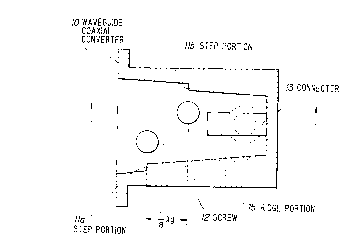
The waveguide coaxial converter 10 comprises step portions
11a, 11b, screws 12 for regulating a capacitive susceptance, a
connector 13 for connecting the converter 10 with a coaxial line,
a center conductor 14 in the connector 13 and a ridge portion 15.
As shown in FIG.2A, the internal sidewalls and internal wide
faces in the waveguide coaxial converter 10 are formed tapered
with being gradually narrowed from an opened end to a bottom
portion. The step portions 11a and 11b formed at both inside
walls are disposed at an interval of ~,g/8. The respective faces
for forming the step portions 11a and 11b are parallel to the
face on the opening of the waveguide coaxial converter 10. A
pair of screws (means for regulating a capacitive susceptance)
12 in which the amount of insertion in the direction of the
internal wide face can be optionally regulated are disposed at
predetermined positions on the internal wide face which
respectively correspond to the positions of the step portions
11a, 11b.
Furthermore, to correct the increase of the cut-off
frequency caused by the step portions 11a, 11b, a ridge portion
15 is formed in nearly the center of the internal wide face. The
ridge portion 15 is, as shown in FIG.2B, provided with a tapered
face in which the thickness is gradually increased in the
direction of the bottom portion, and a flat face extending from
C
-7-
the tapered face to the bottom portion. A center conductor 14
is attached to the flat face of the ridge portion 15.
In the waveguide coaxial converter 10 with such structure,
according as the amount of insertion of the screws 12 is changed,
the damping amount of a high-frequency signal is changed.
Namely, by making the amount of insertion of the screws 12
variable, the load impedance can be varied. Hereon, when the
amount of insertion of the screws 12 is minimized, i.e., in the
case of substantially making no use of the screws 12, an
inductive susceptance becomes predominant as a whole due to the
step portions 11a, 11b formed on the internal sidewall.
Therefore, regulating the capacitive susceptance by the amount
of insertion of the screws 12 makes it possible that the
regulation of the impedance as a whole is performed over the
range from an inductive region to an capacitive region. As a
result, the frequency range where the matching of impedance can
be carried out is significantly enlarged.
On the other hand, since the ridge portion 15 for originally
reducing the cut-off frequency is formed as shown in FIG.2B, it
can be also used for the impedance conversion between the
waveguide and the coaxial line to provide an interface for the
coaxial line. Thereby, the total scale can be reduced.
Moreover, such structure for the impedance conversion
between the waveguide and the coaxial line in this embodiment is
suitable for casting and does not need a supporting material such
as Teflon~ for the center conductor 14. Therefore, a waveguide
coaxial converter for high power can be easily made to reduce the
manufacturing cost.
2~.G3~~Q
_8_
FIG.3 shows a waveguide matching circuit in a preferred
embodiment of the invention. The waveguide matching circuit 20
comprises inductive rods 21a, 21b and screws 22 for regulating
a capacitive susceptance.
As shown in FIG.3, the waveguide matching circuit 20 has the
inductive rods 21a and 21b which are disposed at an interval of
.1g/8 on the internal sidewall, replacing the step portions 11a,
11b in the waveguide coaxial converter 10 as mentioned above .
Further, a pair of screws 22 are disposed on the same planes as
the respective inductive rods 21a, 21b. The screws 22 are the
same ones as the screws 12 in the waveguide coaxial converter as
mentioned above.
In operation, when the amount of insertion of the screws 22
is minimized, i.e., in the case of substantially making no use
of the screws 22, an inductive susceptance becomes predominant
as a whole due to the inductive rods 21a, 21b. Therefore,
regulating the capacitive susceptance by the amount of insertion
of the screws 22 makes it possible that the regulation of the
impedance as a whole is performed over the range from an
inductive region to an capacitive region. As a result, the
frequency range where the matching of impedance can be carried
out is significantly enlarged.
Meanwhile, the number of the step portions 11a, 11b or the
inductive rods 21a, 21b is not limited to two.
Although the invention has been described with respect to
specific embodiment for complete and clear disclosure, the
appended claims are not to be thus limited but are to be
-9-
construed as embodying a11 modification and alternative
constructions that may be occurred to one skilled in the art
which fairly fall within the basic teaching here is set forth.