Note: Descriptions are shown in the official language in which they were submitted.
18-3 CA 2 1 6 3 6 9 2
DESIGN OF AN ELECTRONIC BEAM FORMING NETWORK FOR PHASED
ARRAY APPLICATIONS
Field of the Invention:
This invention relates generally to controlling a beam transmitted from a
phased array
antenna and more particularly to reducing the complexity of the circuitry for
controlling
such a beam.
Background of the Invention:
Phased array antennas are in development for many radar and communication
applications. Some current work in the field of phased array antenna design is
outlined in
Robert J. Mailloux, "Antennas and Radar", Microwave Journal, March 1987, pp.28-
33,
Eli Brookner, "Array Radars: An Update Part II", Microwave Journal, March
1987,
pp.167-174, and Farzin Lalezari, Theresa C. Boone, J. Mark Rogers, "Planar
millimeter-
wave arrays", Microwave Journal, April 1991, pp.85-92. Phased array antennas
offer
several advantages over conventional antennas. For example, beam steering is
possible
without any mechanical movement of an antenna, side-lobe cancellation is
achievable
electronically, two-dimensional scanning becomes more flexible, power
consumption can
be reduced, and phased array antennas have a much higher protection against
catastrophic
failure. However, the large number of transmit/receive modules - in the order
of 10,000
in some cases - forming these phased array antennas presents some demanding
requirements. The signal distribution to and from each antenna element creates
formidable topology, EMI, and crosstalk problems. These problems are discussed
by H.
Wong, S.S. Chang, and T.Q. Ho in "Signal Distribution techniques for active
phased-
array antennas", Microwave Journal, June 1991 pp. 147-154. The phase and
amplitude
control of the signals for each element, is not a trivial matter as discussed
by T.C.
Cheston in "Beam steering of planar phased array", Proceedings of the 1970
phased array
antenna symposium, pp. 219-221.
In current phased array antennas, phase and amplitude control of the transmit
or receive
signals for beam steering and beam nulling is done at the antenna element
according to a
control signal sent by a central processor. This approach presents a number of
drawbacks. First, for an M~N element array, M~N phase and amplitude shifters
are
2163692
18-3 CA Patent
required. Second, the two most critical functions of beam forming, viz. phase
and
amplitude control, are maintained at the antenna element. Knowing that the
performances of phase shifters and variable amplifiers vary with temperature,
sophisticated feedback circuitry must be included at each antenna element
increasing
fabrication costs. Third, RF signals and control signals are distributed to
each antenna
element rendering the distribution network complex.
In an attempt to overcome these limitations, a number of methods have evolved
for beam
steering. In "Introduction to radar system", McGraw-Hill, 1962, p.311, M.
Skolnik
proposes a method of RF frequency scanning where, by changing the transmit
frequency,
the output beam would be steered because of path delay in the distribution
network.
Skolnik indicated how the method could be extended to two dimensions. The
method
however, requires large bandwidth and output frequencies are dependent on the
beam
position.
In "Optical beam forming techniques for phased-array antennas", Microwave
Journal,
July 92, pp. 74-83, A. Seeds proposes a modification to the method of Skolnik,
by
providing an additional signal, which, when mixed with a first signal, removes
the
frequency shift created for beam steering. The method is proposed for a one-
dimensional
array and for the transmit mode of a radar application. The method makes use
of optical
fibres of known lengths for generating path delays.
It is an object of the invention to reduce the number of required phase
shifters and
required control lines and therefore in fabrication cost for a phased array
antenna.
Summary of the Invention:
In accordance with the invention there is provided a method of controlling a
transmit
beam of a phased array antenna comprising the steps of: (a) digitally
computing on a
computer phase and amplitude information of RF signals required at a plurality
of phased
array elements of the antenna to obtain a desired beam shape in a desired
direction; (b)
applying to the RF signals information related to the digitally computed phase
and
amplitude information; (c) converting the RF signals to optical signals; (d)
distribute the
optical signals to interface units of the antenna elements; (e) converting the
distributed
optical signals to electrical signals; and (f) radiating the electrical
signals at the elements.
2
18-3 CA 2 1 6 3 fi 9 2 Patent
In accordance with the invention there is further provided a method of
controlling a
phased array antenna to receive a beam comprising the steps of: (a) digitally
computing
on a computer phase and amplitude information of RF signals required at a
plurality of
phased array elements of the antenna to obtain a desired beam shape in a
desired
direction; (b) applying to the RF signals information related to the digitally
computed
phase and amplitude information; (c) converting the RF signals to optical
signals; (d)
distribute the optical signals to interface units of the antenna elements; (e)
converting the
distributed optical signals to electrical signals; and (f) utilizing the
electrical signals as a
local oscillator to downconvert the received signal to an intermediate
frequency that
corresponds in phase to the information computed in step (a).
In accordance with the invention there is further provided a phased array
antenna having
a plurality of antenna elements disposed in a predetermined pattern for
radiating first RF
signals having relative phase and amplitude characteristics and formed by a
combination
of second signals provided thereto, a method of controlling a beam comprising
the steps
of: (a) digitally computing the phase and amplitude characteristics of the
first RF signals
required at some phased array antenna elements, using a processor; (b)
digitally
computing, for each of some phased array antenna elements, characteristics of
a plurality
of second signals and associating said second signals with said phased array
antenna
element of said some phased array antenna elements wherein a combination of
some of
the plurality of second signals at an associated phased array antenna element
results in
substantially an approximation of the required first RF signal of step (a) and
wherein
some of the second signals associated with a phased array antenna element are
substantially the same as second signals associated with other phased array
antenna
elements; (c) generating the plurality of associated second signals with
characteristics
computed in step (b) for some phased array antenna elements; (d) providing to
some
phased array antenna elements the generated second signals for said phased
array antenna
elements; and (e) from said phased array antenna elements, radiating an RF
signal in
dependence upon a combination of the generated second signals provided
thereto.
In accordance with an embodiment of the invention there is provided a phased
array
antenna having a plurality of antenna elements disposed in a predetermined
pattern for
receiving first RF signals having relative phase and amplitude
characteristics, a method of
controlling a beam comprising the steps of: (a) digitally computing the phase
and
amplitude characteristics of the first RF signals for reception by some phased
array
y '1
..
18-3 CA 1 ,~ z Patent
antenna elements, using a processor; (b) digitally computing, for each of some
phased
array antenna elements, characteristics of a plurality of second signals and
associating
said second signals with said phased array antenna element of said some phased
array
antenna elements wherein a combination of some of the plurality of second
signals at an
associated phased array antenna element results in substantially an
approximation of the
required first RF signal for reception as computed in step (a) and wherein
some of the
second signals associated with a phased array antenna element are
substantially the same
as second signals associated with other phased array antenna elements; (c)
generating the
plurality of associated second signals with characteristics computed in step
(b) for some
phased array antenna elements; (d) providing to some phased array antenna
elements the
generated second signals for said phased array antenna elements; and (e)
filtering signals
received by said phased array antenna elements in dependence upon a
combination of the
generated second signals provided thereto.
In accordance with another embodiment of the invention there is provided a
phased array
antenna comprising: a plurality of antenna elements disposed in a
predetermined pattern
for radiating first RF signals having relative phase and amplitude
characteristics and
formed by a combination of second signals provided thereto; means for
digitally
computing the phase and amplitude characteristics of the first RF signals
required at some
phased array antenna elements; means for digitally computing, for each of some
phased
array antenna elements, characteristics of a plurality of second signals and
associating
said second signals with said phased array antenna element of said some phased
array
antenna elements wherein a combination of some of the plurality of second
signals at an
associated phased array antenna element results in substantially an
approximation of the
required first RF signal as computed in step (a) and wherein some of the
second signals
associated with a phased array antenna element are substantially the same as
second
signals associated with other phased array antenna elements; means for
generating the
plurality of associated second signals; means for providing to some phased
array antenna
elements the generated second signals associated with said phased array
antenna
elements; means for combining the generated second signals; and means for
radiating,
from said phased array antenna elements, an RF signal in dependence upon a
combination
of the generated second signals provided thereto.
4
3 6 9 2 Patent
18-3 CA
Brief Description of the Drawings:
Exemplary embodiments of the invention will now be described in accordance
with the
drawings in which:
Fig. 1 is a graphical presentation of the general geometry showing numeric
symbols used
within the application.
Fig. 2 shows an overall schematic diagram of an optically control array for
radar
applications;
Fig. 3 presents a schematic diagram of a central processor unit for radar
applications;
Fig. 4 shows a schematic diagram of an optical signal distribution network;
Fig. 5 presents a schematic diagram of an antenna element interface unit for
radar
applications;
Fig. 6 shows a schematic diagram of an architecture for a central processor
and
distribution functions for communications applications with a distribution
network
similar to the one shown in Fig. 2; and
Fig. 7 presents a schematic of an antenna element interface unit for
communications
applications.
Detailed Description of the Invention
The present invention describes an improved method of controlling beams in a
phased
array antenna implementation wherein the array has N rows and M columns. An
opto-
electronic architecture is described that allows for beam stirring with fewer
than N~M
phase shifters as are used in the prior art. The opto-electronic architecture
simplifies the
antenna element interface unit (AEIU) by executing the phase control function
in a
central processor unit and hence lowering the fabrication cost and providing
greater
stability of the phase control. Dynamic amplitude control is performed in a
specific
number of locations.
5
18-3 CA
2 1 fi 3 6 9 2 Patent
1. SYSTEM DESCRIPTION
Fig. 1 shows a graphical presentation of the general geometry showing numeric
symbols
used within equation ( 1 ). An N~M array of elements 100 at a plane of an
antenna is
shown. A field at element (n, m) located at (x~, ym), has phase ~(x~, ym) and
amplitude
A",m. A far field pattern of this two-dimensional array antenna in a direction
(a,[3) is
expressed as:
N M 2~ ))
j(2~ft--sin~3~x"cosy+y", sina~+~(x",y",
ECa~ l~) - ~ ~ An~me ~ (1)
n=1 m=t
where;
a angle of far field point measured from the z-axis in the x-z plane
(azimuth angle, taken from antenna plane),
b angle of far field point measured from the y-axis in the y-z plane
(elevation angle from the normal to the antenna plane),
RF mid-band free space wavelength,
Xn along track coordinate of antenna element (n,m)
N number of columns in the antenna,
y", across track coordinate of antenna element (n,m),
M number of rows in the antenna,
w angular frequency of operation (=2~f),
~(xn,y",) phase weight applied to element (n,m),
A~,", amplitude weight applied to element (n,m)
n element number in x-dimension (row number) ranging from 0 to N-1
m element number in y-dimension (column number) ranging from 0 to M-1
f frequency of operation (f = c/~,)
c velocity of electromagnetic wave
6
18-3 CA
2 1 6 3 6 g 2 Patent
From equation (1) it is seen that the phase weight, ~(x~,y",), which must be
applied to the
element (n.m), to have a single beam in the direction of a and (3 is
mathematically
represented by the sum of two phase weights; one defined by the element
position along
track (xn) and the other one by its position across track (y",)
~(xn ~Ym ) _ ~(xn ) '+' ~(Ym ) (2)
wherein
3
~(x" ) _ ~ sin /3x" cos a (along track) ( )
2~ (4)
~( y", ) _ -sin ,~3y", sin a (across track)
Thus, phases for a two-dimensional array are separable into xn and y",.
Equation (2)
expresses that if beam shaping is not needed, no more than one phase shifter
per row and
one per column is needed to steer a beam into a direction defined by (a,~3).
This means
that only (M+l~ phase shifters are needed instead of (M~~ according to the
prior art,
where N is the number of rows and M the number of columns in the antenna.
Further
simplification can be achieved by taking advantage of the linear progression
of the phase
shifts. The separate phases are linearly proportional to the co-ordinates xy~
and yyn. The
separated signals are described below with reference to a signal in a first
direction or
dimension, and a signal in a second direction or dimension. It will be
apparent to one of
skill in the art, that further directions of dimensions are employed when RF
signals are
separated into more than 2 component signals. As will be shown hereafter, only
M RF
phase shifters could be used.
Beam steering to the direction (a, ~ is accomplished on either transmit or
receive by
applying appropriate phase shifts ~(xn, yyyt) to a received or transmitted
signal. Using a
brute force method and according to the prior art, all N~M elements are
provided with a
phase shifter to set phase shifts, ~(xn, yr,.i). Similarly, beam shaping is
accomplished by
appropriately applying amplitude weights, An, yyt. In most radar applications
and in a
number of communication systems, in order to maximize the transmit output
power,
amplitude control is done only on the received signal. Moreover, the amplitude
control is
7
6 3 6 9 2 Patent
18-3 CA
often fixed in one direction (say along track)and dynamically varied in the
other
direction. If this is the case, it may be wise to "hardwire" one set of
amplifiers (along
track) and address only M variable amplifiers, i.e. one per row, instead of
one per
element. If amplitude control can not be separated into along track (x~) and
across track
(ym) settings, variable amplifiers, or attenuators, will be required for every
element, with
the corresponding distribution network.
Skolnik (in "Introduction to Radar Systems", M. Skolnik McGraw-Hill 1962 - pp.
310-
320) proposed an RF frequency scanning technique whereby changing the transmit
frequency, the output beam would be steered because of path delay in the
distribution
network. His method however, required large bandwidth and the output frequency
would
be dependent on the beam position. Seeds in "Optical Beamforming Techniques
for
Phased Array Antennas", Alwyn Seeds Microwave Journal, July 1992 - pp. 74-83,
proposed a modification to the approach of Skolnik by adding a second signal,
which,
when mixed to the first one, at the antenna element, would remove the
frequency shift
created for beam steering. Seed's proposal dealt only with a one-dimensional
array and
was described only for the transmit mode of a radar application.
In accordance with the present invention, the transmit and receive modes for
both radar
and communication applications are described for a two-dimension array
antenna. Figs. 2
to 5 give the schematic diagrams of a system in accordance with the present
invention for
a radar application while Figs. 6 and 7 present schematic diagrams dealing
with a
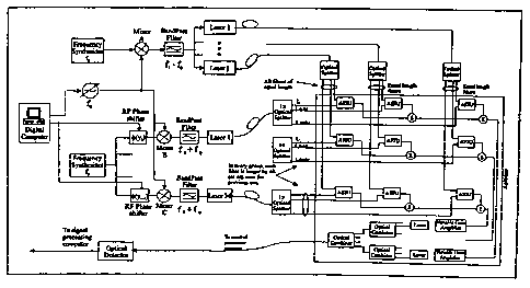
communication system. Fig. 2 shows an overall schematic of an optically
controlled
array antenna for a radar application. It shows the controller section and the
distribution
network to the antenna elements. Figs. 3 to 7 expands for both applications.
Figs. 3 and
6 show the diagram of a central processor unit, for radar and communication
respectively,
where the amplitude and phase weights are computed, and where most of the
signal
conditioning is done (i.e. application of the phase and amplitude weights to
the RF
signals and the RF-to-optics and optics-to-RF interfaces) for the radar and
communication application respectively. Fig. 4 shows the schematic of a signal
distribution network along with an amplitude conditioning group for both
applications.
Figs 5 and 7 show the proposed antenna element interface unit (AEIU).
8
18-3 CA
1 6 3 fi 9 2 Patent
2. RADAR APPLICATIONS
Fig. 2 shows an overall schematic diagram of a proposed architecture. Figs. 3,
4 and 5
expand on the different functions: central processor controller, signal
distribution, and
antenna element.
2.1 C.'entral Processor Controller
The central processor (Fig. 3) for a radar application is responsible for the
computation of
the required amplitude and phase of the RF signals, the application of phase
settings on
the RF signals and to provide the RF-to-optics conversion on transmit and the
optics to
RF conversion on receive.
Three RF frequencies need to be synthesized (Fig. 2). A first frequency fl,
serves as a
frequency reference. A second frequency, f2, (fl +f2 equals the frequency of
operation)
carries the across-track phase information. The third frequency f~, as will be
seen, defines
the along track phase settings. The frequency f~~ is mixed with f, and fz in
conventional
frequency mixers. The lower sideband, f,- f~, produced at mixers A, and the
upper
sideband f2+ f~~ produced at mixers B, are kept. Alternatively, the other
sidebands could
also be used. Those two frequencies are converted to the optical domain by
modulating
the intensity of a laser source. For example, direct modulation of laser
diodes (Fig. 3) or
external modulators can be used. The number of lasers, j, required to carry
frequency
(f~-f~)~ to every antenna element depends on a power budget. The number of
lasers
required to carry frequency (fz-f~)~ equals the number of rows N in the
antenna if direct
modulation is used or depends on the power budget if external modulation is
used. Those
two frequencies are then carried to the antenna elements via a fibre optic
link. At the
antenna elements, they are mixed at mixer C, and the sum frequency, at .f, +.f
, is filtered
by the bandpass filter ( Fig. 5).
The across track phase shifts, ~(Y~")~ are applied to frequency, f2~ through M
conventional
RF phase shifters, ~(Y;), one per row of the antenna. Alternatively, the phase
shifters,
~(yo) to ~(ym_,) are replaced by optical time delays to make the across-track
beam steering
9
21 63692
.- 18-3 CA Patent
frequency independent. The along track phase settings ~(xn), are based on the
value of
f~, and are done using a differential delay network.
Alternatively optical heterodyne techniques are used to generate frequencies
f~ and fZ
allowing optical phase shifters to be used instead of conventional RF ones.
2.2 Distribution Network
As shown in Fig. 4, the along track frequency, (f~-f~)~ is distributed to
every antenna
element in a parallel fashion, that is every signal arrives in phase at every
element. In
accordance with an embodiment of the invention, a most practical mean of
achieving this
is by using a fibre optic distribution network. A waveguide approach would be
much too
complex to implement. The across track frequency, (f2+f~)~ is distributed
sequentially in
each row, with a delay of 0t between each antenna element. Equation 5, giving
the phase
weight of an element (m,n), may then be rewritten as:
~(xn ~Ym ) _ ~CYm ) + 2~(n -1)dt( f2 + f~ ) radians I (5)
0t is related to a path length difference, ~l, through a relation Ot = Ol
*rl/c where rl is the
refractive index of the fiber optic and c is the light velocity. The Ol is
implemented by
incremental increases in fiber length as seen in Fig. 4. It is shown that if
~t = k / f2 where
k is an integer, the frequency f~ required to position the beam in the a,(3
direction is given
by:
d (6)
f~ = f2 sin,Qcosa
C~ok)
where d is the physical antenna element spacing in the along track dimension
and ~, the
free space wavelength of f~+fz. The path length difference, between adjacent
elements in
a row is then taken as Ol = k (c/ rifz).
18-3 CA 2 1 6 3 6 9 2 Patent
It is worth noting that in a frequency agile system, the presented beam
forming network
(BFN) is easily made frequency independent by changing the frequency f~ as the
frequency f, is varied while the frequency f2 remains fixed. In this case, the
M RF phase
shifters also need to be re-addressed but since M is usually small, this is
easily done.
2.3 Antenna Element
Fig. 5 gives the schematic diagram of the AEIU. Under this configuration, the
same BFN
is used for both the transmit and receive signals. Each antenna element
receives, from the
processor unit, two optical signals corresponding to the along track and
across track
information. Those optical signals are converted to the electrical domain by
optical
detectors. The desired RF signal, with proper phase, is obtained by mixing the
two
detected optical signals and filtering the desired sideband (f~+f2). During
transmission,
the RF switch directs the frequency towards the power amplifier and the
radiating
element. During reception, the switch directs that frequency towards the local
oscillator
(LO) port of a front end mixer. The received signal, through a circulator, is
fed to the RF
port of this mixer. Consequently, out of the intermediate frequency (IF) port
(Fig. 5), is
a signal at the difference frequency with a phase equal to the difference
between the
phase of the LO and RF signals. Along track amplitude control may then be
done. Since
the signals of every element are in phase, they may be added together as shown
in Fig. 5.
Moreover, the resulting signal is at an IF level, rendering its distribution
back to the
central processor even easier.
3. COMMUNICATIONAPPLICATIONS
3.1 C.'entral Processor Controller
In some communications applications, the phased array would be expected to
transmit
and receive simultaneously. Therefore the radar architecture described above
would not
be acceptable. Moreover, since in satellite communications, the transmit and
receive
links are done at two different frequencies, the phase and amplitude weights
required for
beam steering must also be different, as shown from equation 1. Two steering
processors
must then be implemented. However, for applications where only one beam is
required at
any time, and when beam shaping is not needed, the functions described in the
radar
11
21 63692
18-3 CA Patent
application can still be used. Phase shifts can be broken down in two separate
sections:
along track and across track and differential time delays can still be used.
Fig. 6 shows the architecture for simultaneous transmit and receive for a
communications
application. If only one of the two function is needed, then the configuration
would be
correspondingly simplified. The information to be transmitted is embedded on
an RF
carrier at frequency f,. This carrier is mixed with a signal f~~ which, as in
the radar
application, provides the along track phase steering for transmission. For the
receive
mode, another RF signal, at frequency f~, is used. This signal is mixed with
f~ to provide
the along track phase shift for the receive mode. The across track phase is
applied using
conventional RF phase shifters on a carrier of frequency fz. Two sets of phase
shifters are
required, one for the transmit beam ~~m and one for the receive beam ~"". The
frequency
f, phase weighted with ~~m, is mixed the frequency f~~, filtered to keep the
one of the
sideband and converted to optics using laser at wavelength ~,,. The frequency
f2, phase
weighted with ~,."" is mixed the frequency fir, filtered to keep the one of
the sideband and
converted to optics using laser at wavelength ~,z. Those two modulated optical
signals are
combined using a wavelength division multiplexing (WDM) combiner and are
distributed
to the antenna elements using the same distribution network as with the radar
application.
If multiple beams are required, one controller per beam is needed. However,
since such a
controller is relatively compact, this should not be a problem.
3.2 Distribution Network
This distribution network could be similar to the one proposed for the radar
application if
wavelength division multiplexing (WDM) is used. Otherwise four optical fibres
would
be needed per antenna element. Consequently, two sets of lasers, at different
wavelengths, are required as shown in Fig. 6.
The optical approach is best suited for multiple beam application since the
same
distribution network can carry the information of every controller described
above.
Wavelength division multiplexing could easily be used and the size and weight
of the
distribution network would not increase.
12
18-3 CA
2 1 6 3 6 9 2 Patent
3.3 Antenna Element
In the AEIU, the four signals now have to be split and mixed accordingly. As
shown in
Fig. 7, wavelength demultiplexers are used and the signals associated with the
transmit
mode are mixed together, filtered, amplified and radiated. The two signals
associated
with the receive mode are also mixed and filtered but are used as the local
oscillator of a
mixer to downconvert the received signal. The intermediate frequency generated
is
filtered and carried back to the central processor in a similar approach than
with the radar
application.
4. CONCL USION
In accordance with the present invention, a novel architecture for the optical
control of
1 S array antennas in a radar and a communication application is described.
The architecture
could readily be implemented with today's technology. The present invention
has several
advantages over conventional RF techniques described in the prior art
references. First,
the present invention simplifies the AEIU by executing the phase control
function in the
central processor unit. This lowers the fabrication cost of the element,
allows better
stability of the phase control and eliminates the need for a distribution
network for the
phase control information. Second, phase control is greatly simplified from
the use of a
frequency synthesis and a differential delay line approach. Third, the
received signal is
downconverted at the antenna element, which allows an improvement in the
signal-to-
noise ratio and dynamic range while reducing the complexity of the
distribution network
for the returned path. Fourth, the received signals, being downconverted and
phased
properly at the antenna elements, are added together, offering "free" gain.
Fifth, the
distribution network is based on fiber optics, allowing a more flexible
network than with
conventional RF waveguides. Sixth, the number of phase shifters is reduced
from one per
element to one per row with the addition of a frequency synthesizer.
5. ADVANTAGES
1. Phase control function is done in the central processor unit.
This lowers the fabrication cost of the element, allows better stability of
the
phase control and eliminates the need for a distribution network for the phase
13
18-3 CA 2 1 6 3 6 9 2 Patent
control information.
2. Phase control is done using a combination of conventional RF phase
shifters, and
with the use of a frequency synthesis and a differential delay line approach.
The RF phase shifters offer a high degree of freedom in the phase weighting
while
the differential delay line reduces the component count.
3. The received signal is downconverted at the antenna element.
The signal-to-noise ratio and the dynamic range are improved.
The complexity of the distribution network for the returned path is reduced.
4. The received signals from the different elements are added in phase in the
distribution network.
5. The distribution network is based on fiber optics, allowing a more flexible
network than with conventional RF waveguides.
6. Wavelength division multiplexing is used to carry the information for beam
steering the transmit and receive beams in the same distribution network.
The above-described embodiments of the invention are intended to be examples
of the
present invention and numerous modifications, variations, and adaptations may
be made
to the particular embodiments of the invention without departing from the
scope and
spirit of the invention, which is defined in the claims.
14