Note: Descriptions are shown in the official language in which they were submitted.
21 63798
CONTROL DEVICE FOR POWER 8AVING
BACKGROUND OF THE I~v~NllON
1. Field of the Invention
The present invention relates to a control device for power
saving for electric and electronic appliances such as personal
computers, printers, etc. which generates a suspension signal or
a power-off signal to save power by detecting a horizontal sync
signal and a vertical sync signal generated in the appliances.
2. Description of the Prior Art
Power saving is a function of electric or electronic
appliances such as personal computers, printers, etc. which can
prevent unnecessary power consumption by automatically putting
the appliance in a power saving mode if the appliance is not used
for a predetermined time. Power saving may be divided into a
suspension mode for providing a power supply for a minimum basic
operation of the appliance and a power-off mode for intercepting
the power supply. In a personal computer, a processor provides
to a control device for power saving a horizontal sync signal and
a vertical sync signal being supplied to a monitor in a normal
mode of operation if a key signal is not entered for a
predetermined time. Then, the control device for power saving
detPcts the sync signals and in combination of the sync signals,
provides to a central processing unit (CPU) a suspension signal
commanding the CPU to go into the suspension mode, or a power-off
signal commanding the CPU to go into the power-off mode.
FIG. 1 is a schematic circuit diagram of a conventional
device for power saving. Referring to FIG. l, the conventional
21 63798
device is provided with a diode D1 for clamping an input
horizontal sync signal Hsync, transistors Q1 and Q2 which are
reversely turned on or off by the horizontal sync signal Hsync
inputted through the diode D1, a diode D6 for clamping an input
vertical sync signal Vsync, transistors Q4 and Q5 which are
reversely turned on or off by the vertical sync signal Vsync
inputted through the diode D6, diodes D2 to D5 and capacitors C2,
C3, and C5 for rectifying and smoothing outputs of the
transistors Q1, Q2, Q4, and Q5, and output transistors Q3, Q6 to
Q8 which are controlled to be turned on or off according to the
rectified and smoothed output signals to provide a suspension
signal SUS or a power-off signal P0.
The numerals C1 and C4 denote coupling capacitors, R1 to R11
denote resistors, and B+ denotes a power supply.
The operation of the conventional control device for power
saving as constructed above will now be explained.
Referring again to FIG. 1, if both the horizontal sync
signal Hsync and the vertical sync signal Vsync are inputted, the
input horizontal sync signal Hsync is clamped through the
capacitor C1 and the diode D1, and the clamped sync signal is
applied to the transistors Q1 and Q2 through the speed-up
capacitor C6 and the resistor R1 to operate the transistors Ql
and Q2. The output of the transistor Q12 is rectified to a
direct current (DC) signal by the diodes D2 and D3 and the
capacitors C2 and C3, and this DC signal is applied to the
transistors Q3 and Q7. The transistor Q3 is turned on by the
voltage rectified by the diode D2 and the capacitor C2, while the
transistor Q7 is turned on by the voltage rectified by the diode
21 637~8
-
D3 and the capacitor C3. If the transistor Q7 is turned on, the
transistor Q8 is turned off.
In the meantime, the input vertical sync signal Vsync is
clamped through the capacitor C4 and the diode D6, and the
clamped sync signal is applied to the transistors Q4 and Q5
through the resistor R6 to operate the transistors Q4 and Q5.
The output of the transistor Q5 is rectified by the diodes D4 and
D5 and the capacitors C3 and C5, and the rectified DC signal is
applied to the transistors Q6 and Q7. The transistor Q6 is
turned on by the DC voltage rectified by the diode D5 and the
capacitor C5, causing the suspension signal SUS to become low.
Also, the transistor Q7 is turned on by the DC voltage rectified
by the diode D4 and the capacitor C3 and the voltage rectified by
the diode D3, causing the power-off signal PO to become low. In
this case, the system is in the normal mode.
In case that the horizontal sync signal Hsync is inputted,
but the vertical sync signal Vsync is not inputted, the
transistor Q6 remains turned off, resulting in that the
transistor Q3 is turned off and the transistor Q7 is turned on.
Accordingly, the suspension signal SUS becomes high, while the
power-off signal PO becomes low, causing the system to go into
the suspension mode. On the contrary, in case that the
horizontal sync signal Hsync is not inputted, but the vertical
sync signal Vsync is inputted, the transistors Q4, Q5, and Q7 are
all turned on, but the transistors Q3 and Q6 are turned off.
Accordingly, the suspension signal SUS becomes high, while the
power-off signal PO becomes low, causing the system also to go
into the suspension mode.
2 1 637~
.
In case that neither the horizontal sync signal Hsync nor
the vertical sync signal Vsync is inputted, the transistors Q1 to
Q3, and Q7 are turned off, and the transistors Q4 to Q6 are
turned off due to the absence of the horizontal and vertical sync
signals Hsync and Vsync. Since the transistor Q7 is turned off,
the transistor Q8 is turned on, and thus the suspension signal
SUS becomes low, while the power-off signal PO becomes high,
causing the system to go into the power-off mode.
However, the conventional control device for power saving as
shown in FIG. 1 has the disadvantage that it has an inferior
transient response characteristic since it is constructed as an
analog circuit. Further, the initial operation of the
conventional device becomes unstable due to the capacitance of
the capacitors employed in the circuit. This causes the
lS reliability of the power saving to deteriorate and integration of
the circuit to be difficult.
SUMMARY OF THE INVENTION
It is an object of the present invention to provide a
control device for power saving which enables integration of the
circuit and improves its transient response characteristic by
constructing the device with a digital circuit.
In order to achieve the above object, the control device for
power saving according to the present invention comprises:
horizontal sync signal input means for providing a
horizontal sync signal synchronized with a system clock signal;
horizontal sync signal detecting means for detecting whether
or not said horizontal sync signal is inputted by counting an
21 63798
output of said horizontal sync signal input means;
horizontal detected signal output means for outputting a
horizontal power-off signal in accordance with an output of said
horizontal sync signal detecting means;
vertical sync signal input means for providing a vertical
sync signal synchronized with said system clock signal;
vertical sync signal detecting means for detecting whether
or not said vertical sync signal is inputted by counting an
output of said vertical sync signal input means;
vertical detected signal output means for outputting a
vertical power-off signal in accordance with an output of said
vertical sync signal detecting means;
control signal output means for outputting a system power-
off signal or a suspension signal for a suspension mode in
accordance with said horizontal power-off signal from said
horizontal detected signal output means and said vertical power-
off signal from said vertical detected signal output means; and
clock generating means for providing said system clock
signal to said horizontal sync signal detecting means and said
vertical sync signal detecting means.
BRIEF DESCRIPTION OF THE DRAWINGS
The above object and other features and advantages of the
present invention will become more apparent by describing the
preferred embodiments thereof with reference to the accompanying
drawings, in which:
FIG. 1 is a schematic circuit diagram of a conventional
control device for power saving.
2 1 63798
FIG. 2 is a schematic circuit diagram of the control device
for power saving according to one embodiment of the present
invention.
FIGs. 3A to 3I are waveform diagrams related to the
horizontal sync signal at various points in FIG. 2.
FIGs. 4A to 4I are waveform diagrams related to the vertical
sync signal at various points in FIG. 2.
FIG. 5 is a schematic circuit diagram of the control device
for power saving according to another embodiment of the present
invention.
DETAILED DESCRIPTION OF THE PREFERRED EMBODIMENT
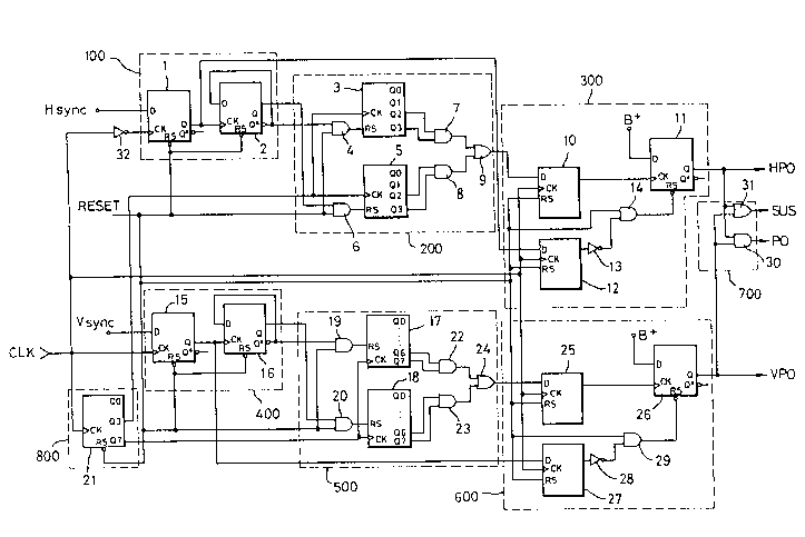
FIG. 2 shows a circuit of the control device for power
saving according to one embodiment of the present invention. The
control device includes a horizontal sync signal input section
100 for synchronizing an input horizontal sync signal Hsync with
a system clock signal CLK and outputting the synchronized
horizontal sync signal, a horizontal sync signal detecting
section 200 for detecting whether or not the horizontal sync
signal Hsync is inputted by counting the output of the horizontal
sync signal input section 100, and a horizontal detected signal
output section 300 for outputting a horizontal power-off signal
HPO in accordance with the horizontal sync signal Hsync outputted
from the horizontal sync signal detecting section 200.
The control device also includes a vertical sync signal
input section 400 for synchronizing an input vertical sync signal
Vsync with the system clock signal CLK and outputting the
synchronized vertical sync signal, a vertical sync signal
21 637~8
detecting section 500 for detecting whether or not the vertical
sync signal Vsync is inputted by counting the output of the
vertical sync signal input section 400, and a vertical detected
signal output section 600 for outputting a vertical power-off
signal VPO in accordance with the vertical sync signal Vsync
outputted from the vertical sync signal detecting section 500.
The control device also includes a control signal output
section 700 for outputting a system power-off signal PO or a
suspension signal SUS in accordance with the horizontal power-off
signal HPO and the vertical power-off signal VPO, and a clock
generating section 800 for generating and providing the system
clock signal to the horizontal sync signal detecting section 200
and the vertical sync signal detecting section 500.
The horizontal sync signal input section 100 comprises a
flip-flop 1 for synchronizing the horizontal sync signal Hsync
with the system clock signal CLK, and a flip-flop 2 being toggled
by the horizontal sync signal Hsync synchronized by the flip-flop
1.
The horizontal sync signal detecting section 200 comprises
counters 3 and 5 for counting the system clock signal CLK in a
period when they are not reset, the counters being reset by the
output of the horizontal sync signal input section 100, AND gates
4 and 6 for resetting the counters 3 and 5 in accordance with a
system reset signal RESET and the non-inverting output of the
flip-flop 2 inputted thereto, AND gates 7 and 8 and an OR gate 9
for detecting the input horizontal sync signal Hsync by combining
the outputs of the counters 3 and 5.
The horizontal detected signal output section 300 comprises
2 1 63798
.,
a monostable multivibrator 10 providing a pulse signal in
accordance with the output of the OR gate 9 in the horizontal
sync signal detecting section 200, a flip-flop 11 receiving the
pulse signal from the monostable multivibrator 10 as its clock
signal and outputting the horizontal power-off signal HPO in
accordance with the horizontal sync signal Hsync, a monostable
multivibrator 12 providing a pulse signal in accordance with the
horizontal sync signal Hsync outputted from the non-inverting
terminal of the flip-flop 1 in the horizontal sync signal input
section 100, an inverter 13 and an AND gate 14 for resetting the
flip-flop 11 in accordance with the output of the monostable
multivibrator 12.
The vertical sync signal input section 400 comprises a flip-
flop 15 for synchronizing the vertical sync signal Vsync with the
system clock signal CLK, and a flip-flop 16 being toggled by the
vertical sync signal Vsync synchronized by the flip-flop 15.
The vertical sync signal detecting section 500 comprises
counters 17 and 18 for counting the system clock signal in a
period when they are not reset, the counters 17 and 18 being
reset by the output of the vertical sync signal input section
400, AND gates 19 and 20 for resetting the counters 17 and 18 in
accordance with the system reset signal RESET and the inverting
output of the flip-flop 16 inputted thereto, AND gates 22 and 23
and an OR gate 24 for detecting the input vertical sync signal
Vsync by combining the outputs of the counters 17 and 18.
The vertical detected signal output section 600 comprises a
monostable multivibrator 25 providing a pulse signal in
accordance with the output of the OR gate 24 in the vertical sync
2 1 63798
signal detecting section 500, a flip-flop 26 receiving the pulse
signal from the monostable multivibrator 25 as its clock signal
and outputting the vertical power-off signal VPO in accordance
with the vertical sync signal Vsync, a monostable multivibrator
27 providing a pulse signal in accordance with the vertical sync
signal Vsync outputted from the non-inverting terminal of the
flip-flop 15 in the vertical sync signal input section 400, an
inverter 28 and an AND gate 29 for resetting the flip-flop 26 in
accordance with the output of the monostable multivibrator 27.
The control signal output section 700 comprises an AND gate
30 for AND-gating the horizontal power-off signal HPO from the
horizontal detected signal output section 300 and the vertical
power-off signal VPO from the vertical detected signal output
section 600 and outputting the system power-off signal PO, and an
OR gate 31 for OR-gating the horizontal power-off signal HPO and
the vertical power-off signal VPO and outputting the suspension
signal SUS.
The clock generating section 800 comprises a decimal counter
21, which performs decimal counting with respect to the system
clock signal CLK, and provides its output Q3 to the counters 3
and 5 and its output Q9 to the counters 17 and 18.
The operation of the control device for power saving
according to the present invention as constructed above will be
explained with reference to FIGs. 2, 3A to 3I, 4A to 4I, and 5.
In case that both the horizontal sync signal Hsync and the
vertical sync signal Vsync are inputted, the control device is
initialized, and then the counter 21 in the clock generation
section 800 performs decimal counting with respect to the system
21 63798
clock signal. The output Q3 of the counter 21 is provided to the
counters 3 and 5 as their clock signal, and the output Q9 of the
counter 21 is provided to the counters 17 and 18 as their clock
signal. Thus, the counters can operate with a timing
synchronized with the clock signal.
If the horizontal sync signal Hsync as shown in FIG. 3I is
inputted to the input terminal D of the flip-flop 1, the
horizontal sync signal Hsync is synchronized with the system
clock signal CLK inverted by the inverter 32, and the
synchronized horizontal sync signal is provided from the output
terminal Q of the flip-flop 1 to the following flip-flop 2 as its
clock signal and to the monostable multivibrator 12 as its input
data.
The flip-flop 2 is toggled by the horizontal sync signal
Hsync, and outputs a signal as shown in FIG. 3A and an inverted
signal as shown in FIG. 3B. The signal as shown in FIG. 3A,
which is outputted from the non-inverting output terminal Q of
the flip-flop 2, is inputted to the reset terminal RS of the
counter 5 through the AND gate 6 to reset the counter 5, and the
inverted signal as shown in FIG. 3B, which is outputted from the
inverting output terminal Q* of the flip-flop 2, is inputted to
the reset terminal of the counter 3 through the AND gate 4 to
reset the counter 3.
The counters 3 and 5 perform countiny operation in a period
when the reset state is released (i.e., in a high-leveled
period). At this time, if the input horizontal sync signal Hsync
exists, the outputs of the AND gates 7 and 8 are kept low as
shown in FIGs. 3C and 3D since the reset-active time of the AND
2 1 637~8
gates 7 and 8 is determined to be shorter than the outputs Q2 and
Q3 of the counters 3 and S. Accordingly, the output of the OR
gate 9 becomes low as shown in FIG. 3E.
Since the output of the OR gate 9 is low, the present state
does not change, and thus the output of the monostable
multivibrator 10 is not generated as shown in FIG. 3F.
Accordingly, the output of the flip-flop 11, which receives the
output of the monostable multivibrator 10 as its clock signal, is
kept low as its initial reset state, causing the horizontal
power-off signal HPO to be low as shown in FIG. 3H. At this
time, the monostable multivibrator 12 receives the horizontal
sync signal Hsync outputted from the flip-flop 1 as its input
data, and provides a pulse signal. This pulse signal is inputted
to the flip-flop 11 as its reset signal through the inverter 13
and the AND gate 14 as shown in FIG. 3G. However, since the
output of the flip-flop 11 has already been low, the reset signal
has no meaning.
The operation of the control device with respect to the
input vertical sync signal Vsync is the same as that with respect
to the input horizontal sync signal Hsync as described above.
If the vertical sync signal Vsync as shown in FIG. 4I is
inputted to the input terminal D of the flip-flop 15, the
vertical sync signal Vsync is synchronized with the system clock
signal CLK, and the synchronized vertical sync signal is inputted
to the following flip-flop 16 as its clock signal and to the
monostable multivibrator 27 as its input data.
The flip-flop 16 is toggled by the input vertical sync
signal Vsync, and output a signal as shown in FIG. 4A and an
2 1 637~8
inverted signal as shown in FIG. 4B. The signal as shown in FIG.
4A, which is outputted from the non-inverting output terminal Q
of the flip-flop 16, is inputted to the reset terminal RS of the
counter 17 through the AND gate 19 to reset the counter 17, while
the inverted signal as shown in FIG. 4B, which is outputted from
the inverting output terminal Q* of the flip-flop 16, is inputted
to the reset terminal of the counter 18 through the AND gate 20
to reset the counter 18.
The counters 17 and 18 perform counting operation in a
period when the reset state is released (i.e., in a high-leveled
period). At this time, if the input vertical sync signal Vsync
exists, the outputs of the AND gates 22 and 23 are kept low as
shown in FIGs. 4C and 4D since the reset-active time of the AND
gates 22 and 23 is determined to be shorter than the outputs Q6
and Q7 of the counters 17 and 18. Accordingly, the output of the
OR gate 24 becomes low as shown in FIG. 4E.
Since the output of the OR gate is low, the present state
does not change, and thus the output of the monostable
multivibrator 25 is not generated as shown in FIG. 4F.
Accordingly, the output of the flip-flop 26, which receives the
output of the monostable multivibrator 25 as its clock signal, is
kept low as its initial reset state, causing the vertical power-
off signal VPO to be low as shown in FIG. 4H. At this time, the
monostable multivibrator 27 receives the vertical sync signal
Vsync outputted from the flip-flop 15 as its input data, and
provides a pulse signal. This pulse sighal is inputted to the
flip-flop 26 as its reset signal through the inverter 28 and the
AND gate 29 as shown in FIG. 4G. However, the output of the
12
21 63798
flip-flop 26 has already been low, and thus the reset signal has
no meaning.
Consequently, the horizontal power-off signal HPO outputted
form the flip-flop 11 and the vertical power-off signal VPO
5 outputted from the flip-flop 26 are inputted to the OR gate 31
and the AND gate 30 in the control signal output section 700,
resulting in that both the suspension signal SUS and the power-
off signal PO outputted from the control signal output section
become low.
10In case that the horizontal sync signal Hsync is not
inputted, but the vertical sync signal Vsync is inputted, the
counters 3 and 5 perform counting operation with the clock signal
provided from the counter 21 in a period when the reset of the
counters 3 and 5 is released. In response to the outputs Q2 and
15Q3 of the counters 3 and 5, the outputs of the AND gates 7 and 8
are shown in FIGs. 3C and 3D. Accordingly, the OR gate 9 outputs
a signal as shown in FIG. 3E to the monostable multivibrator 10
as its data.
The monostable multivibrator 10 outputs a pulse signal as
shown in FIG. 3F in accordance with the system clock signal CLK.
Since the output of the flip-flop 11, which receives the pulse
signal from the monostable multivibrator 10 as its clock signal,
becomes high as shown in FIG. 3H in a period when the horizontal
sync signal Hsync does not exist, the horizontal power-off signal
HPO becomes high and thus the suspension signal SUS outputted
from the OR gate 31 becomes high.
Thereafter, if the horizontal sync signal Hsync is inputted,
the monostable multivibrator 12 generates a pulse signal in
13
21 63798
accordance with the horizontal sync signal outputted from the
flip-flop 1. This pulse signal is provided to the flip-flop 11
through the inverter 13 and the AND gate 14 to reset the flip-
flop 11, resulting in that the horizontal power-off signal HPO
and the suspension signal SUS may be low again.
In case that the horizontal sync signal Hsync is inputted
but the vertical sync signal Vsync is not inputted, the counters
17 and 18 perform counting operation with the clock signal from
the output terminal Q9 of the counter 21 in a period when the
reset of the counters 17 and 18 is released, and the outputs of
the AND gates 22 and 23 are shown in FIGs. 4C and 4D in
accordance with the outputs Q2 and Q3 of the counters 17 and 18.
Accordingly, the OR gate 24 outputs the signal as shown in FIG.
4E to the monostable multivibrator 25 as its input data, and the
monostable multivibrator 25 outputs the pulse signal as shown in
FIG. 4F in accordance with the system clock signal CLK.
The output of the flip-flop 26, which receives the clock
signal from the monostable multivibrator 25 as its clock signal,
becomes high as shown in FIG. 4H in a period when the vertical
sync signal Vsync does not exist, and thus the vertical power-off
signal VPO becomes high, causing the suspension signal SUS
outputted from the OR gate 31 also to become high.
Thereafter, if the vertical sync signal Vsync is inputted,
the monostable multivibrator 27 outputs a pulse signal in
accordance with the vertical sync signal Vsync outputted from the
flip-flop 15. This pulse signal is provided to the flip-flop 26
through the inverter 28 and the AND gate 29 to reset the flip-
flop 26, resulting in that both the vertical power-off signal VPo
21 63798
and the suspension signal SUS may be low again.
In summary, if either the horizontal sync signal Hsync or
the vertical sync signal Vsync is inputted, either of the two
power-off signals HPO and VPO becomes high, resulting in that the
suspension signal SUS outputted from the OR gate 31 becomes high,
and the system power-off signal PO outputted from the AND gate 30
becomes low. In the meantime, neither the horizontal sync signal
Hsync nor the vertical sync signal Vsync is inputted, both the
horizontal power-off signal HPO and the vertical power-off signal
VPO become high, resulting in that both the suspension signal SUS
and the system power-off signal PO become high. The suspension
signal SUS and the system power-off signal PO as described above
is provided to the following control system such as a CPU, so
that the control system controls the appliance to go into the
suspension mode or the system power-off mode.
FIG. 5 shows a circuit of the control device for power
saving according to another embodiment of the present invention.
According to the circuit of FIG. 5, the counter 21 in FIG. 2 is
replaced by a 4:1 (divide-by-4) counter 21a, and the output Q3 of
this counter 2la is provided to the counters 3 and 4 as their
clock signal. Also, an OR gate 2lb is added to OR-gate the input
horizontal sync signal Hsync and the output of the monostable
multivibrator 10. The output of the OR gate 2lb is provided to
the counters 17 and 18 as their clock signal. Referring to FIG.
S, the counter 21a counts the system clock signal CLK and
provides its output signal to the counters 3 and S as their clock
signal as in FIG. 2. The OR gate 2lb provldes the horizontal
sync signal Hsync to the counters 17 and 18 as their clock signal
21 637~8
if the horizontal sync signal Hsync is inputted. If the
horizontal sync signal Hsync is not inputted, the OR gate 21b
provides the output pulse signal of the monostable multivibrator
10 to the counters 17 and 18 as their clock signal, enabling the
5counters 17 and 18 to operate. The counters 17 and 18 can store
more than the 6:1 (divide-by-6) counted value.
From the foregoing, it will be apparent that the control
device for power saving according to the present invention has
the advantages that its transient response characteristic is
10improved and its control reliability is greatly increased since
it is constructed as a digital circuit, not as an analog circuit
as in the convention device, and the existence of the input sync
signal is determined within two-period time of the sync signal.
While the present invention has been described and
15illustrated herein with reference to the preferred embodiments
thereof, it will be understood by those skilled in the art that
various changes in form, details, and applications may be made
wherein without departing from the spirit and scope of the
invention.
16