Note: Descriptions are shown in the official language in which they were submitted.
WO.94/~571 PCT~S93/11845
~i~4~94
AMORPHIC DIAMOND FILM FLAT FIELD EMISSION CATHODE
RELATED APPLICATION
This application is a continuation-in-part of
Serial No. 07/851,701, which was filed on March 16,
1992, entitled "Flat Panel Display Based on Diamond
Thin Films" which application is hereby incorporated
herein by reference.
TECHNICAL FIELD OF THE INVENTION
This invention relates, in general, to flat field
10. emission cathodes and, more particularly, to such
cathodes which employ an amorphic diamond film having a
plurality of emission sites situated on a flat emission
surface.
W094/~571 PCT~S93/11845
~164294
BACKGROUND OF THE INVENTION
Field emission is a phenomenon which occurs when
an electric field proximate the surface of an emission
material narrows a width of a potential barrier
existing at the surface of the emission material. This
allows a quantum tunnelling effect to occur, whereby
electrons cross through the potential barrier and are
emitted from the material. This is as opposed to
thermionic emission, whereby thermal energy within an
emission material is sufficient to eject electrons from
the material. Thermionic emission is a classical
phenomenon, whereas field emission is a quantum
mechanical phenomenon.
The field strength required to initiate field
emission of electrons from the surface of a particular
material depends upon that material's effective "work
function. n Many materials have a positive work
function and thus require a relatively intense electric
field to bring about field emission. Some materials
do, in fact, have a low work function, or even a
negative electron affinity, and thus do not require
intense fields for emission to occur. Such materials
may be deposited as a thin film onto a conductor,
resulting in a cathode with a relatively low threshold
voltage required to produce electron emissions.
In prior art devices, it was desirable to enhance
field emission of electrons by providing for a cathode
geometry which focussed electron emission at a single,
relatively sharp point at a tip of a conical cathode
(called a micro-tip cathode). These micro-tip
cathodes, in conjunction with extraction grids
WO94128571 PCT~S93/11845 -
21642~4
proximate the cathodes, have been in use for years in
field emission displays.
For example, U.S. Patent No. 4,857,799, which
issued on August 15, 1989, to Spindt et al., is
directed to a matrix-addressed flat panel display using
field emission cathodes. The cathodes are incorporated
into the display backing structure, and energize
corresponding cathodoluminescent areas on a face plate.
The face plate is spaced 40 microns from the cathode
arrangement in the preferred embodiment, and a vacuum
is provided in the space between the plate and
cathodes. Spacers in the form of legs interspersed
among the pixels maintain the spacing, and electrical
connections for the bases of the cathodes are diffused
sections through the backing structure. Spindt et al.
employ a plurality of micro-tip field emission cathodes
in a matrix arrangement, the tips of the cathodes
aligned with apertures in an extraction grid over the
cathodes. With the addition of an anode over the
extraction grid, the display described in Spindt et al.
is a triode (three terminal) display.
Unfortunately, micro-tips employ a structure which
is difficult to manufacture, since the micro-tips have
fine geometries. Unless the micro-tips have a
consistent geometry throughout the display, variations
in emission from tip to tip will occur, resulting in
unevenness in illumination of the display.
Furthermore, since manufacturing tolerances are
relatively tight, such micro-tip displays are expensive
to make.
For years, others have directed substantial effort
toward solving the problem of creating cathodes which
WO-94128571 PCT~S93/11845
216~294 4
can be mass manufactured to tight tolerances, allowing
them to perform with accuracy and precision. Another
object of some of these prior art inventions was that
they made use of emission materials having a relatively
low effective work function so as to minimize
extraction field strength.
One such effort is documented in U.S. Patent
No. 3,947,716, which issued on March 30, 1976, to
Fraser, Jr. et al., directed to a field emission tip on
which a metal adsorbent has been selectively deposited.
In a vacuum, a clean field emission tip is subjected to
heating pulses in the presence of an electrostatic
field to create thermal field build up of a selected
plane. Emission patterns from this selected plane are
observed, and the process of heating the tip within the
electrostatic field is repeated until emission is
observed from the desired plane. The adsorbent is then
evaporated onto the tip. The tip constructed by this
process is selectively faceted with the emitting planar
surface having a reduced work function and the non-
emitting planar surface as having an increased work
function. A metal adsorbent deposited on the tip so
prepared results in a field emitter tip having
substantially improved emission characteristics.
Unfortunately, as previously mentioned, such micro-tip
cathodes are expensive to produce due to their fine
geometries. Also, since emission occurs from a
relatively sharp tip, emission is still somewhat
inconsistent from one cathode to another. Such
disadvantages become intolerable when many cathodes are
employed in great numbers such as in a flat panel
display for a computer.
WO941~571 PCT~S93/11845
216~294
--5--
As is evident in the above-described cathode
structure, an important attribute of good cathode
design is to minimize the work function of the material
constituting the cathode. In fact, some substances such
as alkali metals and elemental carbon in the form of
diamond crystals display a low effective work function.
Many inventions have been directed to finding suitable
geometries for cathodes employing negative electron
affinity substances as a coating for the cathode.
For instance, U.S. Patent No. 3,970,887, which
issued on July 20, 1976, to Smith et al., is directed
to a microminiature field emission electron source and
method of manufacturing the same wherein a single
crystal semiconductor substrate is processed in
accordance with known integrated microelectronic
circuit techniques to produce a plurality of integral,
single crystal semiconductor raised field emitter tips
at desired field emission cathode sites on the surface
of a substrate in a manner such that the field emitters
tips are integral with the single crystal semiconductor
substrate. An insulating layer and overlying conductive
layer may be formed in the order named over the
semiconductor substrate and provided with openings at
the field emission locations to form micro-anode
structures for the field emitter tip. By initially
appropriately doping the semiconductor substrate to
provide opposite conductivity-type regions at each of
the field emission locations and appropriately forming
the conductive layer, electrical isolation between the
several field emission locations can be obtained.
Smith et al. call for a sharply-tipped cathode. Thus,
the cathode disclosed in Smith et al. is subject to the
same disadvantages as Fraser, Jr. et al..
WO94/28571 PCT~S93/11845
~64294 ~ -6-
U.S. Patent No. 4,307,507, which issued on
December 29, 1981, to Gray et al., is directed to a
method of manufacturing a field-emitter array cathode
structure in which a substrate of single crystal
material is selectively masked such that the unmasked
areas define islands on the underlying substrate. The
single crystal material under the unmasked areas is
orientation-dependent etched to form an array of holes
whose sides intersect at a crystal graphically sharp
point.
U.S. Patent No. 4,685,996, which issued on August
11, 1987, to Busta et al., is also directed to a method
of making a field emitter and includes an
anisotropically etched single crystal silicon substrate
to form at least one funnel-shaped protrusion on the
substrate. The method of manufacturing disclosed in
Busta et al. provides for a sharp-tipped cathode.
Sharp-tipped cathodes are further described in
U.S. Patent No. 4,885,636, which issued on August 8,
1989, to Busta et al..
Yet another sharp-tipped emission cathode is
disclosed in U.S. Patent No. 4,964,946, which issued on
October 23, 1990, to Gray et al.. Gray et al. disclose
a process for fabricating soft-aligned field emitter
arrays using a soft-leveling planarization technique,
e.g. a spin-on process.
Even though they employ low effective work-
function materials to advantage, sharp-tipped cathodes
have fundamental problems when employed in a flat panel
graphic display environment, as briefly mentioned
above. First, they are relatively expensive to
manufacture. Second, they are hard to manufacture with
WO94/28571 PCT~S93/11845
21~4z94
great consistency. That is, electron emission from
sharp-tipped cathodes occurs at the tip. Therefore,
the tip must be manufactured with extreme accuracy such
that, in a matrix of adjacent cathodes, some cathodes
do not emit electrons more efficiently than others,
thereby creating an uneven visual display. In other
words, the manufacturing of cathodes must be made more
reliable so as to minimize the problem of
inconsistencies in brightness in the display along its
surface.
In Serial No. 07/851,701, which was filed on March
16, 1992, and entitled "Flat Panel Display Based on
Diamond Thin Films," an alternative cathode structure
was first disclosed. Serial No. 07/851,701 discloses a
cathode having a relatively flat emission surface as
opposed to the aforementioned micro-tip configuration.
The cathode, in its preferred embodiment, employs a
field emission material having a relatively low
effective work function. The material is deposited
over a conductive layer and forms a plurality of
emission sites, each of which can field-emit electrons
in the presence of a relatively low intensity electric
field.
Flat cathodes are much less expensive and
difficult to produce in quantity because the fine,
micro-tip geometry has been eliminated. The advantages
of the flat cathode structure was discussed at length
therein. The entirety of Serial No. 07/851,701, which
is commonly assigned with the present invention, is
incorporated herein by reference.
A relatively recent development in the field of
materials science has been the discovery of amorphic
W094/28571 PCT~S93/11845
~6 ~29~ -8-
diamond. The structure and characteristics of amorphic
diamond are discussed at length in "Thin-Film Diamond, n
published in the Texas Journal of Science, vol. 41, no.
4, 1989, by C. Collins et al.. Collins et al.
describe a method of producing amorphic diamond film by
a laser deposition technique. As described therein,
amorphic diamond comprises a plurality of micro-
crystallites, each of which has a particular structure
dependent upon the method of preparation of the film.
The manner in which these micro-crystallites are formed
and their particular properties are not entirely
understood.
Diamond has a negative election affinity. That
is, only a relatively low electric field is required to
distort the potential barrier present at the surface of
diamond. Thus, diamond is a very desirable material
for use in conjunction with field emission cathodes.
In fact, the prior art has employed crystalline diamond
films to advantage as an emission surface on micro-tip
cathodes.
In "Enhanced Cold-Cathode Emission Using Composite
Resin-Carbon Coatings, n published by S. Bajic and R.V.
Latham from the Department of Electronic Engineering
and Applied Physics, Aston University, Aston Triangle,
Burmingham B4 7ET, United Kingdom, received May 29,
1987, a new type of composite resin-carbon
field-emitting cathode is described which is found to
switch on at applied fields as low as approximately 1.5
MV m 1, and subsequently has a reversible I-V
characteristic with stable emission currents of > or =
1 mA at moderate applied fields of typically < or = 8
MV m~l. A direct electron emission imaging technique
has shown that the total externally recorded current
WO94/28571 PCT~S93/11~5
21~4~4
stems from a high density of individual emission sites
randomly distributed over the cathode surface. The
observed characteristics have been qualitatively
explained by a new hot-electron emission mechanism
involving a two-stage switch-on process associated with
a metal-insulator-metal-insulator-vacuum (MIMIV)
emitting regime. However, the mixing of the graphite
powder into a resin compound results in larger grains,
which results in fewer emission sites since the number
of particles per unit area is small. It is preferred
that a larger amount of sites be produced to produce a
more uniform brightness from a low voltage source.
In "Cold Field Emission From CVD Diamond Films
Observed In Emission Electron Microscopy, n published by
C. Wang, A. Garcia, D.C. Ingram, M. Lake and M.E.
Kordesch from the Department of Physics and Astronomy
and the Condensed Matter and Surface Science Program at
Ohio University, Athens, Ohio on June 10, 1991, there
is described thick chemical vapor deposited "CVD"
polycrystalline diamond films having been observed to
emit electrons with an intensity sufficient to form an
image in the accelerating field of an emission
microscope without external excitation. The individual
crystallites are of the order of 1-10 microns. The CVD
process requires 800C for the depositing of the
diamond film. Such a temperature would melt a glass
substrate.
The prior art has failed to: (1) take advantage of
the unique properties of amorphic diamond; (2) provide
for field emission cathodes having a more diffused area
from which field emission can occur; and (3) provide
for a high enough concentration of emission sites
(i.e., smaller particles or crystallites) to produce a
W094/~571 PCT~S93/11845
2~64~9~ -lo-
more uniform electron emission from each cathode site,
yet require a low voltage source in order to produce
the required field for the electron emissions.
WO 94/28571 PCT/US93/1184~
21 ~q29g
SU~ARY OF THE INVENTION
The prior art has failed to recognize that
amorphic diamond, which has physical qualities which
- differ substantially from other forms of diamond, makes
a particularly good emission material. Serial No.
07/851,701 was the first to disclose use of amorphic
diamond film as an emission material. In fact, in the
preferred embodiment of the invention described
therein, amorphic diamond film was used in conjunction
with a flat cathode structure to result in a radically
different field emission cathode design.
The present invention takes the utilization of
amorphic diamond a step further by depositing the
amorphic diamond in such a manner so that a plurality
of diamond micro-crystallite regions are deposited upon
the cathode surface such that at each region (pixel)
there are a certain percentage of the crystals emerging
in an sp2 configuration and another percentage of the
crystals emerging in an SP3 configuration. The
numerous sp2 and SP3 configurations at each region
result in numerous discontinuities or interface
boundaries between the configurations, with the sp2 and
SP3 crystallites having different electron affinities.
Accordingly, to take advantage of the above-noted
opportunities, it is a primary object of the present
invention to provide an independently addressable
cathode, comprising a layer of conductive material and
a layer of amorphic diamond film, functioning as a low
effective work-function material, deposited over the
conductive material, the amorphic diamond film
comprising a plurality of distributed localized
electron emission sites, each sub-site having a
WO94t28571 PCTtUS93/11845
12-
plurality of sub-regions with differing electron
affinities between sub-regions.
In a preferred embodiment of the present
invention, the amorphic diamond film is deposited as a
relatively flat emission surface. Flat cathodes are
easier and, therefore, less expensive to manufacture
and, during operation of the display, are easier to
control emission therefrom.
A technical advantage of the present invention is
to provide a cathode wherein emission sites have
electrical properties which include discontinuous
boundaries with differing electron affinities.
Another technical advantage of the present
invention is to provide a cathode wherein emission
sites contain dopant atoms.
Yet another technical advantage of the present
invention is to provide a cathode wherein a dopant atom
is carbon.
Yet a further technical advantage of the present
invention is to provide a cathode wherein emission
sites each have a plurality of bonding structures.
Still yet another technical advantage of the
present invention is to provide a cathode wherein one
bonding structure at an emission site is SP3.
Still a further technical advantage of the present
invention is to provide a cathode wherein each emission
site has a plurality of bonding orders, one of which is
SP3.
W O 94128571 PCTrUS93/11845
2~642~4
Another technical advantage of the present
invention is to provide a cathode wherein emission
sites contain dopants of an element different from a
low effective work-function material. In the case of
use of amorphic diamond as the low effective work-
function material, the dopant element is other than
carbon.
Still another technical advantage of the present
invention is to provide a cathode wherein emission
sites contain discontinuities in crystalline structure.
The discontinuities are either point defects, line
defects or dislocations.
The present invention further includes novel
methods of operation for a flat panel display and use
of amorphic diamond as a coating on an emissive wire
screen and as an element within a cold cathode
fluorescent lamp.
In the attainment of the above-noted features and
advantages, the preferred embodiment of the present
invention is an amorphic diamond film cold-cathode
comprising a substrate, a layer of conductive material,
an electronically resistive pillar deposited over the
substrate and a layer of amorphic diamond film
deposited over the conductive material, the amorphic
diamond film having a relatively flat emission surface
comprising a plurality of distributed micro-crystallite
electron emission sites having differing electron
affinities.
The foregoing has outlined rather broadly the
features and technical advantages-of the present
-invention in order that the detailed description of the
invention that follows may be better understood.
W094128571 PCT~S93/11845
14-
Additional features and advantages of the invention
will be described hereinafter which form the subject of
the claims of the invention. It should be appreciated
by those skilled in the art that the conception and the
specific embodiment disclosed may be readily utilized
as a basis for modifying or designing other structures
for carrying out the same purposes of the present
invention. It should also be realized by those skilled
in the art that such equivalent constructions do not
depart from the spirit and scope of the invention as
set forth in the appended claims.
WO94/28571 PCT~S93/11845
21~42~4
BRIEF DESCRIPTION OF THE DRAWINGS
For a more complete understanding of the present
invention, and the advantages thereof, reference is now
made to the following descriptions taken in conjunction
with the accompanying drawings, in which:
FIGURE l is a cross-sectional representation of
the cathode and substrate of the present invention;
FIGURE 2 is a top view of the cathode of the
present invention including emission sites;
FIGURE 3 is a more detailed representation of the
emission sites of FIGURE 2;
FIGURE 4 is a cross-sectional view of a flat panel
display employing the cathode of the present invention;
FIGURE 5 is a representation of a coated wire
matrix emitter;
FIGURE 6 is a cross-sectional view of a coated
wire;
FIGURE 7 is a side view of a florescent tube
employing the coated wire of FIGURE 6;
FIGURE 8 is a partial section end view of the
fluorescent tube of FIGURE 7; and
FIGURE 9 is a computer with a flat-panel display
that incorporates the present invention.
WO94128571- PCT~S93/11845
6 ~9 A -16-
DETAILED DESCRIPTION OF THE INVENTION
Turning now to FIGURE 1, shown is a cross-
sectional representation of the cathode and substrate
of the present invention. The cathode, generally
designated 10, comprises a resistive layer 11, a low
effective work-function emitter layer 12 and an
intermediate metal layer 13. The cathode 10 sits on a
cathode conductive layer 14 which, itself, sits on a
substrate 15. The structure and function of the layers
11, 12, 13 of the cathode 10 and the relationship of
the cathode 10 to conductive layer 14 and substrate 15
are described in detail in related application Serial
No. 07/851,701, which is incorporated herein by
reference.
Turning now to FIGURE 2, shown is a top view of
the cathode 10 of FIGURE 1. The emitter layer 12 is,
in the preferred embodiment of the present invention,
amorphic diamond film comprising a plurality of diamond
micro-crystallites in an overall amorphic structure.
The micro-crystallites result when the amorphic diamond
material is deposited on the metal layer 13 by means of
laser plasma deposition, chemical vapor deposition, ion
beam deposition, sputtering, low temperature deposition
(less than 500 degrees Centigrade), evaporation,
cathodic arc evaporation, magnetically separated
cathodic arc evaporation, laser acoustic wave
deposition or similar techniques or a combination of
the above whereby the amorphic diamond film is
deposited as a plurality of micro-crystallites. One
such process is discussed within ~Laser Plasma Source
of Amorphic Diamond,~ published by the American
Institute of Physics, January 1989, by C.B. Collins, et
al.
wog4/28s71 PCT~S93/11845
-17- 21 ~4294
The micro-crystallites form with certain atomic
structures which depend on environmental conditions
during deposition and somewhat on chance. At a given
environmental pressure and temperature, a certain
percentage of crystals will emerge in an sp2
(two-dimensional bonding of carbon atoms)
configuration. A somewhat smaller percentage, however,
will emerge in an SP3 (three-dimensional bonding)
configuration. The electron affinity for diamond
micro-crystallites in an SP3 configuration is less than
that for carbon or graphite micro-crystallites in an
sp2 configuration. Therefore, micro-crystallites in
the SP3 configuration have a lower electron affinity,
making them "emission sites. n These emission sites (or
micro-crystallites with an SP3 configuration) are
represented in FIGURE 2 as a plurality of black spots
in the emitter layer 12.
The flat surface is essentially a microscopically
flat surface. A particular type of surface morphology,
however, is not required. But, small features typical
of any polycrystalline thin film may improve emission
characteristics because of an increase in enhancement
factor. Certain micro-tip geometries may result in a
larger enhancement factor and, in fact, the present
invention could be used in a micro-tip or npeaked"
structure.
Turning now to FIGURE 3, shown is a more detailed
view of the micro-crystallites of FIGURE 2. Shown is a
plurality of micro-crystallites 31, 32, 33, 34, for
example. Micro-crystallites 31, 32, 33 are shown as
having an sp2 configuration. Micro-crystallite 34 is
shown as having an SP3 configuration. As can be seen
WO94/~571 PCT~S93/11845
~ 4 -18-
in FIGURE 3, micro-crystallite 34 is surrounded by
micro-crystallites having an sp2 configuration.
There are a very large number of randomly
distributed localized emission sites per unit area of
the surface. These emission sites are characterized by
different electronic properties of that location from
the rest of the film. This may be due to one or a
combination of the following conditions:
l) presence of a doping atom (such as carbon) in
the amorphic diamond lattice;
2) a change in the bonding structure from sp2 to
SP3 in the same micro-crystallite;
3) a change in the order of the bonding structure
in the same micro-crystallite;
4) an impurity (perhaps a dopant atom) of an
element different from that of the film material;
5) an interface between the various micro-
crystallites;
6) impurities or bonding structure differences
occurring at the micro-crystallite boundary; or
7) other defects, such as point or line defects or
dislocations.
The manner of creating each of the above conditions
during production of the film is well known in the art.
One of the above conditions for creating
differences in micro-crystallites is doping. Doping of
amorphic diamond thin film can be accomplished by
interjecting elemental carbon into the diamond as it is
being deposited. When doping with carbon, micro-
crystallites of different structures will be created
statistically. Some micro-crystallites will be n-type.
Alternatively, a non-carbon dopant atom could be used,
WO94128571 PCT~S93/11845
21 ~4~9~;~
--19--
depending upon the desired percentage and
characteristics of emission sites. Fortunately, in the
flat panel display environment, cathodes with as few as
1 emission site will function adequately. However, for
optimal functioning, 1 to 10 n-type micro-crystallites
per square micron are desired. And, in fact, the
present invention results in micro-crystallites less
than 1 micron in diameter, commonly 0.1 micron.
Emission from the cathode 10 of FIGURE 1 occurs
when a potential difference is impressed between the
cathode 10 and an anode (not shown in FIGURE 1) which
is separated by some small distance from the cathode
10. Upon impression of this potential, electrons are
caused to migrate to the emission layer 12 of the
cathode 10.
In the example that follows, the condition that
will be assumed to exist to create micro-crystallites
of different work function will be a change in the
bonding structure from sp2 to SP3 in the same micro-
crystallite (condition 3 above). With respect to theemission sites shown in FIGURES 2 and 3, micro-
crystallites having an SP3 configuration have a lower
work-function and electron affinity than micro-
crystallites having an sp2 configuration. Therefore,
as voltage is increased between the cathode 10 and
anode (not shown), the voltage will reàch a point at
which the SP3 micro-crystallites will begin to emit
electrons. If the percentage of SP3 micro-crystallites
on the surface of the cathode 10 is sufficiently high,
then emission from the SP3 micro-crystallites will be
sufficient to excite the anode (not shown), without
having to raise voltage levels to a magnitude
sufficient for emission to occur from the sp2 micro-
WO94/~571 PCT~S93/11845
~64~ 20-
crystallites. Accordinqly, by controlling pressure,
temperature and method of deposition of the amorphic
diamond film in a manner which is well-known in the
art, SP3 micro-crystallites can be made a large enough
percentage of the total number of micro-crystallites to
produce sufficient electron emission.
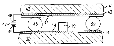
Turning now to FIGURE 4, shown is a cross-
sectional view of a flat panel display employing the
cathode of the present invention. The cathode 10,
still residing on its cathode conductive layer 14 and
substrate 15 as in FIGURE 1, has been mated to an
anode, generally designated 41 and comprising a
substrate 42, which in the preferred embodiment is
glass. The substrate 42 has an anode conductive layer
43 which, in the preferred embodiment, is an indium tin
oxide layer. Finally, a phosphor layer 44 is deposited
on the anode conductive layer to provide a visual
indication of electron flow from the cathode 10. In
other words, when a potential difference is impressed
between the anode 41 and the cathode 10, electrons
flowing from the cathode 10 will flow toward the anode
conductive layer 43 but, upon striking the phosphor
layer 44, will cause the phosphor layer to emit light
through the glass substrate 42, thereby providing a
visual display of a type desirable for use in
conjunction with computers or other video equipment.
The anode 41 is separated by insulated separators 45,
46 which provide the necessary separation between the
cathode 10 and the anode ~1. This is all in accordance
with the device described in Serial No. 07/851,701.
Further, in FIGURE 4, represented is a voltage
source 47 comprising a positive pole 48 and a negative
pole 49. The positive pole is coupled from the source
WO 94128571 PCT~S93/11845
21 64294
-21-
47 to the anode conductive layer 43, while the negative
pole 49 is coupled from the source 47 to the cathode
conductive layer 14. The device 47 impresses a
potential difference between the cathode 10 and the
anode 41, causing electron flow to occur between the
cathode 10 and the anode 41 if the voltage impressed by
the source 47 is sufficiently high.
Turning now to FIGURE 9, there is illustrated
computer 90 with associated keyboard 93, disk drive 94,
hardware 92 and display 91. The present invention may
be employed within display 91 as a means for providing
images and text. All that is visible of the present
invention is anode 41.
Turning now to FIGURE 5, shown is a representation
of a coated wire matrix emitter in the form of a wire
mesh, generally des.gnated 51. The wire mesh 51
comprises a plurality of rows and columns of wire which
are electrically joined at their intersection points.
The wire mesh 51 is then coated with a material having
a low effective work-function and electron affinity,
such as amorphic diamond, to thereby produce a wire
mesh cathode for use in devices which previously used
an uncoated wire or plate cathode and application of a
high current and potential difference to produce
incandescence and a flow of electrons from the mesh to
an anode. By virtue of the amorphic diamond coating
and its associated lower work function, incandescence
is no longer necessary. Therefore, the wire mesh 51
cathode can be used at room temperature to emit
electrons,
Turning now to FIGURE 6, shown is a cross-section
of a wire which has been coated with a material having
WO94128571 PCT~S93/11845
-22-
a low work-function and electron affinity. The wire,
designated 61, has a coating 62 which has been
deposited by laser plasma deposition, or any one of the
other well-known techniques listed above to thereby
permit the coating 62 to act as a cold cathode in the
same manner as the cathodes described in FIGURES 1-5.
Turning now to FIGURE 7, shown is one application
of the wire 61 in which the coated wire 61 functions as
a conductive filament and is surrounded by a glass tube
72, functioning as an anode and which has an electrical
contact 73 to thereby produce a fluorescent tube. The
tube functions in a manner which is analogous to the
flat panel display application discussed in connection
with FIGURES 1-5, that is, a potential difference is
impressed between the wire 61 (negative) and the tube
72 sufficient to overcome the space-charge between the
cathode wire 61 and the tube anode 72. Once the space-
charge has been overcome, electrons will flow from
emission site SP3 micro-crystallites in the coating 62.
Turning now to FIGURE 8, shown is a partial
section end view of the florescent tube 71 of FIGURE 7.
Shown again are the wire 61 and the coating 62 of
FIGURE 6 which, together, form a low effective work-
function cathode in the fluorescent tube 71. The glass
tube 72 of FIGURE 7 comprises a glass wall 81 on which
is coated an anode conductive layer 82. The anode
conductive layer 82 is electrically coupled to the
electrical contact 73 of FIGURE 7. Finally, a phosphor
layer 83 is deposited on the anode conductive layer 82.
When a potential difference is impressed between the
cathode wire 61 and the anode conductive layer 82,
electrons are caused to flow between the emitter
coating 82 and the anode conductive layer 82. However,
W094128571 PCT~S93/11845
2164,~9~
-23-
as in FIGURE 4, the electrons strike the phosphor layer
83 first, causing the phosphor layer 83 to emit photons
through the glass wall 81 and outside the florescent
tube 71, thereby providing light in a manner similar to
conventional fluorescent tubes. However, because the
fluorescent tube of FIGURES 7 and 8 employs a cathode
having a low effective work-function emitter, such as
amorphic diamond film, the fluorescent tube does not
get warm during operation. Thus, the energy normally
wasted in traditional fluorescent tubes in the form of
heat is saved. In addition, since the heat is not
produced, it need not be later removed by air
conditioning.
Although the present invention and its advantages
have been described in detail, it should be understood
that various changes, substitutions and alterations can
be made herein without departing from the spirit and
scope of the invention as defined by the appended
claims.