Note: Descriptions are shown in the official language in which they were submitted.
~164492 CA
CFO 11059
Method of Driving Semiconductor Laser with
Wide Modulation Band, Optical Communication
Method, Semiconductor Laser Device, Node,
and Optical Communication System
BACKGROUND OF THE INVENTION
Field of the Invention
The present invention relates to a semiconductor
laser and, more particular, to modulation of a
semiconductor laser.
Related Backqround Art
Recently, a large transmission capacity is desired
in the field of optical communications, and so optical
frequency division multiplexing (optical FDM)
transmission by which a plurality of wavelengths or
optical frequencies are multiplexed into a single
optical fiber has been developed.
The technologies of optical FCM can be roughly
classified into two categories in accordance with the
reception method: one is coherent optical communication
which forms and detects an intermediate frequency by
taking a beat with a station light source; the other is
a method which transmits and detects only light having
a desired wavelength (frequency) through a tunable
filter.
As the tunable filter, a Mach-Zehnder filter, a
fiber Fabry-Pérot filter, an AO modulation filter, and
216~92
a semiconductor filter have been developed.
It is important to decrease the wavelength
interval in order to increase the transmission capacity
as large as possible. For this purpose, it is
desirable to decrease the transmission band width of
the tunable filter and decrease the occupied frequency
band or the spectral line width of a laser as a light
source. For example, a semiconductor DFB filter with a
tunable width of 3 nm has a transmission band width of
approximately 0.03 nm, so it is ideally possible to
multiplex 100 channels. However, in this case, the
spectral line width of a light source is required to be
0.03 nm or smaller. At present, even a DFB laser known
as a semiconductor laser which oscillates in a dynamic
single mode gives rise to a dynamic wavelength
variation when directly modulated by ASK. Since this
results in an increased spectral line width of about
0.3 nm, a DFB laser is unsuitable for such wavelength
multiplex transmission.
Examples of the methods which have been devised to
suppress this wavelength variation are the use of an
external intensity modulator (e.g., Suzuki et al.;
"~/4-Shift DFB Laser/Absorption Modulator Integrated
Light Source", The Institute of Electronics,
Information and Communication Engineers, Technical
report of IEICE, OQE90-45, p. 99, 1990), a direct FSK
modulation method (e.g., M. J. CHAWKI et al.; "1.5
216~492
Gbit/s FSK TRANSMISSION SYSTEM USING TWO ELECTRODE DFB
LASER AS A TUNABLE FSK DISCRIMINATOR/PHOTODETECTOR",
ELECTRON LET., Vol. 26, No. 15, p. 1146, 1990), and a
direct polarization modulation method (Japanese
Laid-Open Patent Application No. 2-159781).
Comparison of these three methods will be
described below. A wavelength variation of the
external modulator is approximately 0.03 nm, and this
is the marginal performance meeting the specifications.
However, the external modulator is unpreferable in
respect of cost because the number of components is
increased. In the FSK method a file on the receiver
side is sometimes functioned as a wavelength
discriminator, and this requires a complicated control
technique.
The polarization modulation method uses a
two-electrode laser as illustrated in Fig. 1. As shown
in Fig. 2A, a bias current is fixed to a point at which
TE and TM modes are switched, and I1 is modulated with a
weak rectangular current ~I1. Consequently, the planes
of polarization are switched as illustrated in Fig. 2B.
A polarizer arranged at the output end of the laser as
shown in Fig. 1 selects one of these polarization
planes, thereby performing ASK. In this method, the
number of components is not increased because only the
number of electrodes of a conventional DFB laser is
increased, and a wavelength variation is smaller than
~16~492
-- 4 --
that in the external modulation method. Also, since a
signal is transmitted by ASK, the method has an
advantage in that the load on, e.g., a file on the
receiver side is small.
As described above, the polarization modulation is
a modulation method suitable for wavelength multiplex
transmission and the like. Unfortunately, the
conventional proposals do not contain much mention of
the method of driving polarization modulation, so it is
necessary to first establish the driving method to put
this polarization modulation into practical use.
The polarization modulation method performs ASK
modulation by applying a rectangular signal to one
electrode of a multi-electrode DFB laser to thereby
switch TE- and TM-polarized waves, and extracting one
of these polarized waves by using a polarizer arranged
at the exit end. It is unfortunate that the modulation
characteristics deteriorate at low frequencies of 1 MHz
or lower.
Fig. 3 shows the relationship between a modulation
frequency and a modulation factor after this frequency
transmits through the polarizer when the current I1 of
the two-electrode DFB laser in Fig. 1 is modulated with
a sine-wave current. Fig. 4 shows the relationship
between the modulation frequency and the phase
difference (the phase difference between a modulation
current and a modulation optical signal) under the same
2164492
-- 5 --
conditions. As shown in Figs. 3 and 4, a dip of the
modulation factor takes place near several hundred kHz,
and the phase varies below 1 MHz and shows an
opposite-phase response near DC. This is because, due
to a physical factor of polarization modulation of a
laser, polarization switching is done by the combined
effect of a refractive index change resulting from
opposite-phase heat having a cutoff at a few MHz and a
refractive index change caused by an in-phase carrier
density which is flat up to a resonance frequency.
Since the effect of heat becomes dominant at low
frequencies, the flatness of the phase characteristic
is lost as described above.
The above characteristic gives rise to the
following problem. The polarization modulation
primarily transmits digital signals, and the pulse
width is wavelength-converted below 1 MHz to result in
a transmission error. Examples are shown in Figs. 5A
and 5B: a pulse narrowing occurs at a pulse width of
1 MHz in Fig. 5A, and an opposite-phase pulse is formed
at 100 kHz in Fig. 5B. Accordingly, low frequencies
are limited, and this limits the degree of freedom of
coding.
SUMMARY OF THE INVENTION
The present invention has been made in
consideration of the above situation, and has as its
2164492
-- 6
object to broaden the modulation band of polarization
modulation particularly to low frequencies, improve the
degree of freedom of coding, and reduce an error rate
even with a long continuous code, thereby enabling
transmission with a higher density.
To achieve this object the present invention,
there is disclosed a semiconductor laser driving method
of driving a semiconductor laser having two or more
electrodes by switching two polarization modes with
different planes of polarization, comprising the steps
of:
injecting a main modulation current into one of
the electrodes; and
injecting a sub-modulation current whose phase is
adjusted with respect to the main modulation current
into at least one of the electrodes except for the
electrode into which the main modulation current is
injected. Preferred modes of this driving method are
as follows.
The step of injecting the sub-modulation current
is executed when a frequency of the switching is lower
than a predetermined frequency.
The predetermined frequency is approximately
1 MHz.
The phase and/or a modulation amplitude of the
sub-modulation current is so adjusted as to decrease a
phase difference between the main modulation current
216~2
and an output optical signal from the semiconductor
laser.
The phase of the sub-modulation current is so
adjusted as to be the same phase as or an opposite
phase to a phase of the main modulation current.
Whether the phase of the sub-modulation current is
to be the same phase as or an opposite phase to the
phase of the main modulation current is determined in
accordance with whether a sign of a slope of a boundary
line, which is determined by an orthogonal coordinate
system of the sub-modulation current and the main
modulation current, and on which the two polarization
modes of the semiconductor laser are switched, is
positive or negative.
A ratio of modulation amplitudes of the
sub-modulation current and the main modulation current
is so adjusted that a slope of a boundary line, which
is determined by an orthogonal coordinate system of the
sub-modulation current and the main modulation current,
and on which the two polarization modes of the
semiconductor laser are switched, is substantially
parallel to a synthetic amplitude of the sub-modulation
current and the main modulation current on the
orthogonal coordinate system.
Also, as an optical communication method using
this driving method, the present invention discloses a
method of performing optical communication by obtaining
~164492
- 8 -
an intensity-modulated signal by selecting one
polarization mode from the output from a semiconductor
laser device driven by the above driving method, and
further discloses an optical communication method of
performing wavelength multiplexing.
The present invention discloses a semiconductor
laser device for outputting two polarization modes with
different planes of polarization by switching the two
polarization modes, comprislng:
a semiconductor laser having two or more
electrodes;
means for injecting a main modulation current into
one of the electrodes of the semiconductor laser; and
means for injecting a sub-modulation current whose
phase is adjusted with respect to the main modulation
current into at least one of the electrodes except for
the electrode into which the main modulation current is
injected. Preferred modes of this semiconductor laser
device are as follows.
The sub-modulation current is injected when a
frequency of the switching is lower than a
predetermined frequency.
The predetermined frequency is approximately
1 MHz.
The device further comprises:
a modulation power supply; and
means for supplying an output from the modulation
2164492
power supply to the means for injecting the main
modulation current and the means for injecting the
sub-modulation current.
The means for injecting the sub-modulation current
has a frequency characteristic and does not inject the
sub-modulation current if a frequency of the output
from the modulation power supply exceeds a
predetermined frequency.
The predetermined frequency is approximately
1 MHz.
The semiconductor laser is a distributed feedback
laser including a diffraction grating near an optical
waveguide containing a light-emitting layer,
so that the light-emitting layer contains a
quantum well structure, and
a wavelength corresponding to an energy band gap
between an energy level of a light hole and a ground
level of an electron in a quantum well of the quantum
well structure is close to a Bragg wavelength of the
diffraction grating.
Threshold gains at the Bragg wavelength in the two
polarization modes are substantially equal.
The quantum well structure is a strained quantum
well structure into which a strain is introduced, so
that in a quantum well an energy level of a light hole
and an energy level of a heavy hole are equal or the
energy level of a light hole is closer to a ground
~16~2
-- 10 --
level of an electron.
The strain is a tensile strain introduced into an
internal quantum well of the quantum well structure.
The quantum well structure is a multiple quantum
well structure.
As a more practical mode of the semiconductor
laser device, the present invention discloses a
semiconductor laser device for outputting two
polarization modes with different planes of
polarization by switching the polarization modes,
comprising:
a semiconductor laser having two or more
electrodes;
a modulation power supply;
first injecting means for passing an output from
the modulation power supply through a first amplifier
and injecting the output as a first modulation current
into one of the electrodes of the semiconductor laser;
and
second injecting means for passing the output from
the modulation power supply through a second amplifier
and injecting the output as a second modulation current
into at least one of the electrodes except for the
electrode into which the first injecting means injects
the first modulation current,
wherein a cutoff frequency of the second amplifier
is a predetermined frequency, and the second modulation
2164~92
current is not injected if a frequency of the output
from the modulation power supply exceeds the
predetermined frequency. More detailed modes of this
semiconductor laser device are as follows.
The outputs from the first and second amplifiers
have the same phase.
The outputs from the first and second amplifiers
have opposite phases.
The predetermined frequency is approximately
1 MHz.
A ratio of gains of the first and second
amplifiers is so adjusted as to decrease a difference
between a phase of the main modulation current and a
phase of an output optical signal from the
semiconductor laser.
As a similarly practical mode of the semiconductor
laser device, the present invention discloses a
semiconductor laser for outputting two polarization
modes with different planes of polarization by
switching the polarization modes, comprising:
a semiconductor laser having two or more
electrodes;
a modulation power supply;
first injecting means for passing an output from
the modulation power supply through a first
voltage-current converter, DC-coupling an output from
the first voltage-current converter and a first DC
2164~92
- 12 -
current, and injecting the resultant current as a first
modulation current into one of the electrodes of the
semiconductor laser; and
second injecting means for passing the output from
the modulation power supply through a second
voltage-current converter, DC-coupling an output from
the second voltage-current converter and a second DC
current, and injecting the resultant current as a
second modulation current into at least one of the
electrodes except for the electrode into which the
first injecting means injects the first modulation
current,
wherein the second injecting means has a low-pass
filter with a predetermined cutoff frequency for
filtering the output from the second voltage-current
converter, and the second modulation current is not
injected if a frequency of the output from the
modulation power supply exceeds the predetermined
frequency. More detailed modes of this semiconductor
device are as follows.
The first and second voltage-current converters
DC-couple the output from the modulation power supply
at the same phase.
The first and second voltage-current converters
DC-couple the output from the modulation power supply
at opposite phases.
The predetermined frequency is approximately
2164492
1 MHz.
A ratio of gains of the first and second
voltage-current converters is so adjusted as to
decrease a difference between a phase of the main
S modulation current and a phase of an output optical
signal from the semiconductor laser.
Also, as a node using the above semiconductor
laser device, the present invention discloses a node
having polarization mode selecting means for
selectively outputting one of the two polarization
modes from the output from the semiconductor laser
device.
Furthermore, the present invention discloses an
optical communication system using the above node as a
node for transmitting information.
As described above, in the present invention, two
modulation currents are injected into different
electrodes of a multi-electrode semiconductor laser
(when the modulation frequency of polarization
modulation is low).
The relationship between the phases of these two
modulation currents slightly change in accordance with
the polarization switching characteristics of the
device. Generally, in the case of a semiconductor
laser with a structure which is largely influenced by
heat, the distributions of TE and TM oscillation modes
with respect to I1/I2 are as shown in Fig. 17; the slope
2164 192
- 14 -
of the boundary line between the TE and TM oscillation
modes is positive. That is, when a DC bias is fixed
near the switching point of polarization, polarization
switching from TE to TM occurs if Il is increased, and
polarization switching from TM to TE occurs if I2 is
increased. Accordingly, the phase of one polarization
switching is opposite to the phase of the other with
respect to the changes in Il and I2. Therefore, when a
modulation current in phase with AI1 is applied as AI2,
the direction of thermal polarization switching becomes
opposite to that of AI1, and this suppresses the thermal
polarization switching with respect to ~Il. The
amplitude ratio of ~Il to ~I2 at this time is preferably
the one illustrated in Fig. 17, which is parallel to
the switching line of polarization.
Although various methods are possible as the means
for generating this in-phase signal, it is only
necessary to take account of low frequencies from DC to
a few MHz. For example, as illustrated in Fig. 9, a
signal is divided into two signal components by a power
divider, one signal component is passed through a
wide-band inverting amplifier, and the other is passed
through an inverting amplifier with a cutoff frequency
of about a few MHz. These signals are then passed
through biases T each consisting of L and C and
superposed on the electrodes of a laser by a DC current
and AC coupling. Referring to Fig. 9, the laser is
~6QQ!)2
- 15 -
expressed as two parallel diodes.
Alternatively, high-speed current driver chips are
used as illustrated in Fig. 10. In this configuration,
two signals are used to drive the respective electrodes
in such a manner that one signal is directly used and
the other is passed through a low-pass filter with a
cutoff frequency of a few MHz. As in Fig. 10, each
driver chip is a parallel integrated circuit of a
modulation current source Ip and a DC bias current
source Ib. In this arrangement, no low-frequency
cutoff of a modulation current exists since there is no
bias T, so it is possible to drive up to DC.
Furthermore, the circuit can be mounted on a small
circuit board and can also be modularized into a single
box together with a laser.
On the other hand, the effect of heat is sometimes
small depending on the structure of a semiconductor
laser. A device of this sort exhibits a polarization
switching characteristic shown in Fig. 18 which is
contrary to that shown in Fig. 17; that is, the slope
of the boundary line between TE and TM oscillation
modes is negative. If this is the case, in contrast to
the case described previously, opposite-phase signals
are used as ~Il and ~I2.
BRIEF DESCRIPTION OF THE DRAWINGS
Fig. 1 is a perspective view for explaining the
2164492
- 16 -
principle of polarization modulation of a conventional
example;
Figs. 2A and 2B are graphs for explaining the
principle of polarization modulation of the
conventional example;
Fig. 3 is a graph showing the polarization
modulation characteristic of the conventional example;
Fig. 4 is a graph showing the phase characteristic
of the conventional example;
Figs. 5A and 5B are timing charts showing the
response waveforms of polarization modulation of the
conventional example;
Fig. 6 is a perspective view showing a
semiconductor laser used in the first to third
embodiments and a portion of a driving current
injecting means used in these embodiments;
Fig. 7 is a graph showing the phase characteristic
when polarization modulation is performed in the first
and third embodiments;
Fig. 8 is a graph showing the phase characteristic
when polarization modulation is performed in the second
embodiment;
Fig. 9 is a circuit diagram showing the
configuration of a semiconductor laser driver in the
first and third embodiments;
Fig. 10 is a circuit diagram showing the
configuration of a semiconductor laser driver in the
~16~492
- 17 -
second embodiment;
Fig. 11 is a perspective view showing a
semiconductor laser used in the fourth embodiment and a
portion of a driving current injecting means used in
the embodiment;
Fig. 12 is a graph showing the tuning
characteristic of the semiconductor laser used in the
first embodiment;
Fig. 13 is a view showing the arrangement of a
transmission system when wavelength multiplex
transmission is performed in the fifth embodiment;
Fig. 14 is a view showing the configuration of a
node in the sixth embodiment;
Fig. 15 is a view showing an example of the
arrangement of an optical LAN;
Fig. 16 is a view showing an example of the
arrangement of an optical CATV system;
Fig. 17 is a graph showing the oscillation mode
distributions of TE and TM modes of a semiconductor
laser with a large thermal effect;
Fig. 18 is a graph showing the oscillation mode
distributions of TE and TM modes of a semiconductor
laser with a small thermal effect;
Figs. l9A and l9B are graphs showing the
oscillation mode distributions of TE and TM modes,
respectively, of the semiconductor laser in the first
embodiment; and
2154~92
- 18 -
Figs. 20A and 20B are graphs showing the
oscillation mode distributions of TE and TM modes,
respectively, of the semiconductor laser in the third
embodiment.
DETAILED DESCRIPTION OF THE PREFERRED EMBODIMENTS
(First Embodiment)
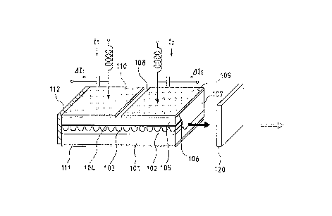
Fig. 6 is a perspective view of a two-electrode
DFB laser for realizing the driving method of the
present invention. Fig. 9 is a circuit diagram for
explaining the configuration of a driver of this
embodiment.
Referring to Fig. 6, this two-electrode DFB laser
includes an n-InP substrate 101, an n-InP buffer layer
102 in which a diffraction grating 0.05 ,um in depth is
formed, a 0.2-,um thick n-InGaAsP (band-gap wavelength
~g = 1.17 ,um) lower optical guide layer 103, an active
layer 104 with a strained superlattice structure
consisting of five 10-nm thick i-InO29Ga071As well
layers and five 10-nm thick i-InGaAsP (~g = 1.17 ,um)
layers, a p-InP cladding layer 105, a p-InO53Ga047As
contact layer 106, a high-resistance InP buried layer
107, an electrode isolation region 108 from which the
contact layer 106 is removed, a Cr/AuZnNi/Au layer 109
as an electrode, a Cr/AuZnNi/Au layer 110 as an
electrode, an AuGeNi/Au layer 111 as a substrate
electrode, and an SiO film 112 as an antireflection
2164~92
-- 19 --
film. In this DFB laser, the active layer serves as a
multiple quantum well layer with a tensile strain, and
the transition energy between the light-hole level and
the electron ground level and the transition energy
between the heavy-hole level and the electron ground
level are so designed as to be equal. Consequently,
the oscillation threshold value in TM polarization is
lower than that in conventional DFB lasers. This makes
an efficient polarization switching feasible. A laser
having a similar arrangement is disclosed in Japanese
Patent Application No. 5-310592. In order for the
distributed feedback wavelength by the diffraction
grating 103 to be close to the wavelength corresponding
to the band gap between the light-hole level and the
electron ground level, the pitch of the diffraction
grating is set at 240 nm so that the diffraction
grating has a Bragg wavelength at 1.562 ,um in a TE mode
and at 1.558 ,um in a TM mode.
In this configuration, switching between TE and TM
occurs as described previously when DC biases of 35 mA
and 28 mA are flowed through the electrodes 109 and
110, respectively, and a digital signal ~I1 with an
amplitude of 5 mA is superposed on the electrode 110.
Also, when a sine-wave signal ~I1 with an amplitude of 5
mA is superposed, the resultant modulation frequency
dependences are as shown in Figs. 3 and 4; although the
modulation factor is within 3 dB at 100 Hz to 1 GHz,
216~92
- 20 -
the phase difference rotates below 1 MHz. This is
because the thermal effect is greatly dominant at low
frequencies as described earlier in "SUMMARY OF THE
INVENTION".
By using the device configuration as illustrated
in Fig. 9, therefore, a modulation current ~I2 as a
sub-current with respect to the main modulation current
~I1 is flowed through the electrode 109. More
specifically, a signal from a modulation current 409 is
divided into two signal components by a 1 : 1 power
divider 408. One signal component is passed through a
wide-band inverting video amplifier 406 with a gain of
10 and a cutoff frequency fc of 10 GHz, superposed on a
DC current from a DC power supply 403 by a bias T 402
with a low cutoff frequency of 1 kHz, and driven as a
driving current I1 + ~I1 for a laser 401. The other
output from the power divider is passed through an
inverting operational amplifier 407 with a gain of 10
and a cutoff frequency fc of 1 MHz, superposed on a DC
current from a DC power supply 405 by a bias T 404, and
driven as a driving current I2 + ~I2 for the laser 401.
In this configuration, the currents ~I1 and AI2 are in
phase with each other because both the amplifiers 406
and 407 are of an inverting output type. Also, the
modulation power supply is of a variable output type,
and the modulation factor is adjusted by the power
supply. The gain ratio of the amplifiers 406 and 407
2164492
is so optimized as to suppress the thermal effect at
low frequencies and is determined in accordance with
the TE/TM oscillation characteristics (to be described
later) of this device and because the division ratio of
the power divider is 1 : 1. This current ratio needs
to be optimized for each individual device, since it
changes in accordance with the composition, the
structure, the material, and the mounting form of the
device. Although the cutoff frequency of the amplifier
406 is set at 10 GHz in this embodiment, this cutoff
frequency can be arbitrarily chosen in accordance with
the modulation frequency.
The distributions of TE and TM oscillation modes
of this device are as illustrated in Figs. l9A and l9B,
respectively, with respect to I1/I2. That is, when a DC
bias is fixed near the switching point of polarization,
polarization switching from TE to TM occurs if I1 is
increased, and polarization switching from TM to TE
occurs if I2 is increased. Accordingly, the phase of
one polarization switching is opposite to the phase of
the other with respect to the changes in I1 and I2.
Therefore, when a modulation current in phase with AI1
is applied as ~I2, the direction of thermal polarization
switching becomes opposite to that of ~I1, and this
suppresses the thermal polarization switching with
respect to ~I1. The amplitudes of ~I1 and ~I2, i.e., in
this embodiment, the gains of the amplifiers 406 and
~16~492
- 22 -
407, are equal so that the synthetic slope of ~I1 and
~Iz is 1, since the slope of the boundary line between
the TE and TM oscillation modes is 1 in Figs. l9A and l9B.
When polarization modulation was performed by this
driving method, a phase characteristic which was flat
down to low frequencies, i.e., a few kHz, was obtained
as shown in Fig. 7, i.e., the low-frequency
characteristic was greatly improved. This enabled
polarization modulation using a rectangular-wave signal
with a pulse width of a few kHz to a few GHz, i.e.,
made ASK transmission possible.
(Second Embodiment)
Fig. 10 is a circuit diagram for explaining the
second embodiment of the present invention. In
Fig. 10, the configuration of a driver different from
that in the first embodiment is illustrated. A device
used is a two-electrode DFB laser which is nearly
identical with that used in the first embodiment.
In this embodiment, a bias T having a
low-frequency cutoff is not used, and modulable laser
driver ICs 503 and 504 are used to decrease the overall
dimensions of the driving system. As indicated by
reference numerals 503 and 504 in Fig. 10, each driver
IC is a parallel integrated circuit of a DC current
source Ib and a modulation current source Ip. Upon
receiving a modulating signal of an ECL level (which is
a voltage pulse with an amplitude of -0.9 V to -1.8 V
~16 ~ 49223
and is an input signal for driving Emitter Coupled
Logic (ECL) as a high-speed driver IC), this driver IC
can drive a modulation current having a DC offset
current. The IC can control the modulation factor and
the bias current quantity.
A practical driving method will be described
below. An output from a modulation power supply 505
having an ECL output is input to the driver ICs 503 and
504. If the modulation power supply voltage is to be
divided into two components, this is performed
immediately before the two drivers. This obviates the
need for a power divider. The driver ICs 503 and 504
extract in-phase outputs from the modulation input.
One output is passed through a low-pass filter with a
cutoff of 1 MHz and driven as a driving current I2 + ~I2
for a laser 501. The other is directly driven as a
driving current I1 + ~I1 for the laser 501. The
amplitude ratio of the modulation currents is optimized
to 1 : 1 as in the first embodiment. As shown in
Fig. 10, it is desirable that each driver IC extract a
current with the laser suspended from the ground since
this makes a high-speed operation possible. In this
embodiment, therefore, the conductivity types of the
device components are reversed, i.e., the device has a
p-type substrate and an n-type electrode on the
electrode isolation side.
With this driving system, the overall system can
2164492
- 24 -
be greatly miniaturized and modularized into a single
box. Also, in the first embodiment, the low frequency
is limited in the band of the bias T, whereas in this
embodiment, there is no limit on low frequencies. This
can further improve the low-frequency characteristics.
That is, as illustrated in Fig. 8, it was possible to
flatten the phase characteristic over a broad range
from 100 Hz to 1 GHz. In ASK transmission, this
permits coding using an NRZ signal having a degree of
continuation of 22 - 1 or more at several Gbps, making
very-high-density transmission possible.
(Third Embodiment)
This embodiment uses a device having a structure
nearly identical with the structures of the
semiconductor lasers used in the first and second
embodiments and having a different composition from the
compositions of these semiconductor lasers.
Since the structure of the device is almost the
same as those in the first and second embodiments, the
composition of the device will be described below with
reference to Fig. 6. Referring to Fig. 6, this device
includes an n-InP substrate 101, an n-InP buffer layer
102 in which a diffraction grating 0.05 ~m in depth is
formed, a 0.2-~m thick n-InGaAsP (band-gap wavelength
~g = 1.3 ,um) lower optical guide layer 103, an active
layer 104 with a strained superlattice structure
consisting of five 8-nm thick i-InO4GaO6As well layers
216449~
- 25 -
and five 10-nm thick i-InGaAsP (~g = 1.3 ,um) barrier
layers, a p-InP cladding layer 105, a p-InOs3GaO47As
contact layer 106, a high-resistance InP buried layer
107, an electrode isolation region 108 from which the
contact layer 106 is removed, a Cr/AuZnNi/Au layer 109
as an electrode, a Cr/AuZnNi/Au layer 110 as an
electrode, an AuGeNi/Au layer 111 as a substrate
electrode, and an SiO film 112 as an antireflection
film. In this DFB laser, the active layer serves as a
multiple quantum well layer with a tensile strain. In
order for the distributed feedback wavelength by the
diffraction grating 103 to be close to the wavelength
corresponding to the band gap between the light hole
level and the electron ground level, the pitch of the
diffraction grating is set at 240 nm so that the
diffraction grating has a Bragg wavelength at 1.562 ,um
in a TE mode and at 1.558 ,um in a TM mode.
In this configuration, switching between TE and TM
occurs as described previously when DC biases of 35 mA
and 21 mA are flowed through the electrodes 109 and
110, respectively, and a digital signal ~I1 with an
amplitude of 5 mA is superposed on the electrode 110.
Also, when a sine-wave signal ~I1 with an amplitude of 5
mA is superposed, the resultant modulation frequency
dependences are as shown in Figs. 3 and 4; although the
modulation factor is within 3 dB at 100 Hz to 1 GHz,
the phase difference rotates below 1 MHz. This is
2164492
- 26 -
because the thermal effect is greatly dominant at low
frequencies as described earlier in "SUMMARY OF THE
INVENTION".
As in the first embodiment, therefore, by using
the method as illustrated in Fig. 9, a modulation
current ~I2 as a sub-current is flowed through the
electrode 109. However, in this embodiment an
amplifier 406 is of an inverting type and an amplifier
407 is of a non-inverting type. More specifically, a
signal from a modulation current 409 is divided into
two signal components by a 1 : 1 power divider 408.
One signal component is passed through the wide-band
inverting video amplifier 406 with a gain of 30 and a
cutoff frequency of 10 GHz, superposed on a DC current
from a DC power supply 403 by a bias T 402 with a low
cutoff frequency of l kHz, and driven as a driving
current I1 + ~I1 for a laser 401. The other output from
the power divider is passed through the non-inverting
operational amplifier 407 with a gain of 20 and a
cutoff frequency of l.MHz, superposed on a DC current
from a DC power supply 405 by a bias T 404, and driven
as a driving current I2 + ~I2 for the laser 401. In
this configuration, the modulation power supply is of a
variable output type, and the modulation factor is
adjusted by the power supply. The gain ratio of the
amplifiers 406 and 407 is so optimized as to suppress
the thermal effect at low frequencies and is thus
216 ~ 27 -
determined because the amplitude ratio of the main
modulation current AI1 to the sub-modulation current AI2
is to be 3 : 2. This current ratio needs to be
optimized for each individual device, since it changes
in accordance with the composition, the structure, the
material, and the mounting form of the device.
The distributions of TE and TM oscillation modes
of this device are as illustrated in Figs. 20A and 20B,
respectively, with respect to I1/I2. That is, when a DC
bias is fixed near the switching point of polarization,
polarization switching from TE to TM occurs if I1 is
increased, and polarization switching from TM to TE
occurs if I2 is increased. Accordingly, one
polarization switching is in phase with the other with
respect to the changes in I1 and I2. Therefore, when a
modulation current having an opposite phase to that of
~I1 is applied as ~I2, the direction of thermal
polarization switching becomes opposite to that of ~
and this suppresses the thermal polarization switching
with respect to ~I1. Since the slope of the boundary
line between the TE and TM oscillation modes is -2/3,
AI1/~I2 = -2/3.
When polarization modulation is performed by this
driving method, a phase characteristic which is flat
down to low frequencies, i.e., a few kHz, is obtained
as in the first embodiment, i.e., the low-frequency
characteristic is greatly improved. This enables
2164~92
- 28 -
polarization modulation using a rectangular-wave signal
with a pulse width of a few kHz to a few GHz, i.e.,
makes ASK transmission possible.
(Fourth Embodiment)
The fourth embodiment of the present invention
will be described below with reference to Fig. 11.
Fig. 11 is a perspective view of a semiconductor DFB
laser of this embodiment. Although the arrangement of
layers is identical with that in the first embodiment,
this laser has a three-electrode structure in which an
electrode in the central portion has a phase adjustment
region from which an active layer is removed. This
further improves the controllability of polarization
switching.
The laser includes an n-InP substrate 201, an
n-InP buffer layer 202 in which a diffraction grating
0.05 ~m in depth is formed, a 0.2-~m thick n-InGaAsP
(band-gap wavelength ~g = 1.17 ~m) lower optical guide
layer 203, an active layer 204 with a strained
superlattice structure consisting of five 10-nm thick
i-InO29GaO71As well layers and five 10-nm thick
i-InGaAsP (~g = 1.17 ~m) layers, a p-InP cladding layer
205, a p-InOs3GaO47As contact layer 206, a
high-resistance InP buried layer 207, electrode
isolation regions 208 and 208' from which the contact
layer 206 is removed, Cr/AuZnNi/Au layers 209 and 209'
as electrodes, a Cr/AuZnNi/Au layer 210 as an
'~164492
- 29 -
electrode, an AuGeNi/Au layer 211 as a substrate
electrode, and SiO films 212 and 212' as antireflection
films.
In the central portion from which the active layer
is removed, the contact layer, the cladding layer, and
the active layer are etched away, and an i-InGaAsP
(~g = 1.17 ,um) optical guide layer 213, a p-InP
cladding layer 214, and a p-InOs3GaO47As contact layer
215 are formed by selective regrowth. The grating
pitch and the like are the same as in the first
embodiment.
A current driving method is as follows. A DC bias
current I2 is flowed through the electrodes 209 and 209'
on the two sides, and a DC bias I1 and a modulation
current ~I1 are flowed through the central electrode
210. When I2 = 60 mA and I1 = 20 mA, it was possible to
superpose a digital signal of ~I1 = 2 mA and perform
TE/TM polarization switching.
In the semiconductor laser of this embodiment,
compared to the semiconductor layer in the first
embodiment, only the phase can be controlled in the
phase adjustment region of the central electrode
without changing the gain, and the influence of heat is
also decreased. Consequently, it was possible to
predict that the distributions of TE and TM oscillation
modes were as shown in Fig. 18 and the slope of the
boundary line was negative. Therefore, ~Il/AI2 was
21644~2
- 30 -
optimized by flowing a polarization switching
characteristic compensating current ~Iz having an
opposite phase to that of ~I1. The result was that
~ I2 was optimized when ~ I2 = 5. Although the
method of driving ~I1 and ~I2 is analogous to that in
the first or second embodiment, the phases of ~I1 and
AI2 are made opposite to each other. Accordingly, if
the driver of the first embodiment is to be used, a
non-inverting type amplifier is used as the operational
amplifier 407 with a cutoff frequency of 1 MHz. If the
driver of the second embodiment is to be used, the
modulation outputs from the driver ICs 503 and 504 are
so set as to have opposite phases.
In this embodiment, ~ I2 is optimized without
obtaining actual TE and TM oscillation modes. However,
as in each embodiment described above, it is also
possible to obtain the boundary line between the TE and
TM oscillation distributions and determine ~ I2 so
that ~ I2 is parallel to the boundary line.
Also, in the above embodiments, the InP-based
lasers have been described. However, the present
invention can be similarly realized even by using some
other material such as a GaAs-based material.
(Fifth Embodiment)
The fifth embodiment of the present invention
makes use of the tunability of a laser in order to
perform wavelength multiplex transmission. The
~164~92
oscillation wavelength of the two-electrode DFB laser
of the first embodiment can be changed by controlling
the values of currents to be flowed into the two
electrodes. Fig. 12 shows the resultant tunability
characteristic. When a current I1 is changed from 30 mA
to 50 mA while the boundary line between TE and TM in
Figs. l9A and l9B, i.e., the relationship of
l.l.I1 - I2 = 10 mA is held constant, the oscillation
wavelength can be continuously changed by approximately
2 nm from 1.556 ~m to 1.554 ,um.
A method of performing wavelength multiplex
communication by using the driving method of the
present invention will be described below with
reference to Fig. 13. An optical communication light
source 801 is polarization-modulated by the present
invention. The wavelength of this light source can be
changed in the range of 2 nm as described above. In
polarization modulation, dynamic wavelength modulation
called chirping, which is a problem in regular direct
intensity modulation, is very small, 2 GHz or less, in
obtaining an extinction ratio (about 10 dB) which is
necessary for transmission. Therefore, in performing
wavelength multiplexing, an interval of 10 GHz
(approximately 0.05 nm) gives no crosstalk to each
adjacent channel. Accordingly, when this light source
is used, wavelength multiplexing of about 2/0.05 = 40
channels is possible.
216~192
- 32 -
The emitted light from this light source is
coupled to a single-mode fiber 802 and transmitted to a
receiver having an optical filter 803 and a
photodetector 804. From the signal light transmitted
through the optical fiber, the optical filter 803
selects and demultiplexes a light component having a
desired wavelength, and the photodetector 804 performs
signal detection. In this embodiment, the optical
filter has the same structure as the DFB laser used in,
e.g., the first embodiment, and the current is biased
to be lower than the threshold value. As with the DFB
laser, by changing the current ratio of the two
electrodes, the transmission wavelength can be changed
by about 2 nm while the transmission gain is held at 20
dB. The transmission width of this filter whose gain
is reduced by 10 dB is about 0.03 nm, i.e., the filter
has an enough characteristic to perform wavelength
multiplexing at intervals of 0.05 nm as described
above. As this optical filter, it is also possible to
use a Mach-Zehnder filter or a fiber Fabry-Pérot filter
enumerated in "Related Background Art". Additionally,
although the laser of this embodiment includes only one
light source and one receiver, transmission can be
performed by coupling several light sources or several
receivers through optical couplers.
Furthermore, when a three-electrode structure such
as described in the fourth embodiment is used as the
~164492
- 33 -
DFB laser, it is possible to broaden the tuning range
and thereby further increase the degree of wavelength
multiplexing.
(Sixth Embodiment)
Fig. 14 shows an example of the configuration of a
photoelectric converter (node) connected to a terminal
when the optical communication light source driving
method of the present invention and an optical
communication system using the method are applied to a
wavelength multiplexing optical LAN system. Fig. 15
shows an example of the configuration of an optical LAN
system using the node.
An optical signal is input to the node through an
optical fiber 901 connected to individual components.
A divider 902 feeds a portion of the input signal to a
receiver 903 including a tunable filter such as
described in the fifth embodiment. As this tunable
filter, it is possible to use, e.g., a fiber
Fabry-Pérot filter, a Mach-Zehnder filter, or an
interference film filter. The receiver performs signal
detection by extracting only an optical signal having a
desired wavelength. To transmit an optical signal from
the node, on the other hand, a tunable DFB laser 904 is
driven to perform polarization modulation as described
in the first to fourth embodiments. The intensity of
the output is modulated by a polarizer and an isolator
905. The resultant light is fed into the light
2164492
- 34 -
transmission line via the divider 906.
If the tuning range needs to be further broadened,
it is only necessary to provide a plurality of tunable
lasers.
The network of the optical LAN system shown in
Fig. 15 is a bus-type network in which a large number
of networked terminals and centers can be accommodated
by connecting nodes in the directions of A and B. To
connect a large number of nodes, however, an optical
amplifier for compensating for an optical attenuation
must be arranged in series with the transmission line.
Also, bidirectional optical transmission using a DQDB
method is possible when two nodes are connected to each
terminal to form two transmission lines.
Furthermore, as the form of the network, it is
possible to apply a loop network in which A and B in
Fig. 15 are connected, a star network, or a composite
form of these networks.
(Seventh Embodiment)
The present invention can construct a wavelength
multiplexing CATV having a topology as illustrated in
Fig. 16. In the CATV center, a tunable laser is
polarization-modulated by the method of any of the
first to fourth embodiments of the present invention
and used as a wavelength multiplexing light source.
Each subscriber as the reception side uses a receiver
including the tunable filter described in the fifth
~164492
- 35 -
embodiment. Conventionally, it is difficult to apply a
DFB filter to such a system due to the influence of a
dynamic wavelength variation of a DFB laser. The
present invention makes this application feasible.
Furthermore, each subscriber is given an external
modulator, and a signal from a given subscriber is
received by reflected light from the modulator (one
form of simple bidirectional optical CATV, e.g.,
Ishikawa and Furuta, "Bidirectional Transmission LAN
External Modulator in Optical CATV Subscriber System",
The Institute of Electronics, Information and
Communication Engineers, Technical report of IEICE,
OCS91-82, p. 51, 1991). When a star network such as
shown in Fig. 16 is constructed in this way,
bidirectional CATV is realized, and this improves the
functions of service.
In the present invention, as has been described
above, two modulation currents whose phase relationship
is adjusted are injected into different electrodes of a
multi-electrode semiconductor laser. Consequently, the
modulation band of polarization modulation is widened
particularly to low frequencies without providing the
semiconductor laser with any special means. Since this
improves the degree of freedom of coding, the error
rate of reception is reduced even with a long
continuous code, and thereby higher-density
transmission is made possible. It is also possible to
2164492
- 36 -
suitably determine the relationship between the phases
of the two modulation currents and the amplitudes of
the two modulation currents. Furthermore, since the
cutoff frequencies and the output characteristics
(e.g., the difference between an inverting output and a
non-inverting output) of amplifiers used in a laser
driver are used, the two modulation currents can be
injected by a simple, low-cost driver. Additionally,
since a voltage-current converter is used in the laser
driver, the gain effect of the converter can be
utilized, and the modulation band can be greatly
widened to low frequencies. Moreover, in optical
communication, a wavelength variation is small even
when the modulation band is widened, so high-density
wavelength multiplexing is possible.