Language selection

Search

Patent 2164711 Summary

Third-party information liability

Some of the information on this Web page has been provided by external sources. The Government of Canada is not responsible for the accuracy, reliability or currency of the information supplied by external sources. Users wishing to rely upon this information should consult directly with the source of the information. Content provided by external sources is not subject to official languages, privacy and accessibility requirements.

Claims and Abstract availability

Any discrepancies in the text and image of the Claims and Abstract are due to differing posting times. Text of the Claims and Abstract are posted:

  • At the time the application is open to public inspection;
  • At the time of issue of the patent (grant).
(12) Patent Application: (11) CA 2164711
(54) English Title: A PHOSPHOR COATING ARRANGEMENT FOR AN ELECTRODELESS DISCHARGE LAMP
(54) French Title: COUCHE DE PHOSPHORE POUR LAMPE A DECHARGE SANS ELECTRODE
Status: Deemed Abandoned and Beyond the Period of Reinstatement - Pending Response to Notice of Disregarded Communication
Bibliographic Data
(51) International Patent Classification (IPC):
  • H01J 65/04 (2006.01)
  • H01J 61/42 (2006.01)
  • H01J 61/56 (2006.01)
(72) Inventors :
  • ROWLEY, ANDREW TERRENCE (United Kingdom)
(73) Owners :
  • GE LIGHTING LIMITED
(71) Applicants :
  • GE LIGHTING LIMITED (United Kingdom)
(74) Agent: CRAIG WILSON AND COMPANY
(74) Associate agent:
(45) Issued:
(86) PCT Filing Date: 1995-04-06
(87) Open to Public Inspection: 1995-10-19
Examination requested: 2002-03-28
Availability of licence: N/A
Dedicated to the Public: N/A
(25) Language of filing: English

Patent Cooperation Treaty (PCT): Yes
(86) PCT Filing Number: PCT/GB1995/000799
(87) International Publication Number: GB1995000799
(85) National Entry: 1995-12-07

(30) Application Priority Data:
Application No. Country/Territory Date
9407128.9 (United Kingdom) 1994-04-11

Abstracts

English Abstract


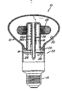
An electrodeless discharge lamp (10) having a lamp envelope (12)
containing a fill of mercury and a rare gas is excitable to a discharge state
by introduction of RF energy in close proximity thereto. A ballast circuit
contained within the housing base portion (22) of the lamp is effective
for generating the RF energy from conventional line power. The ballast
circuit includes a core portion which extends within a re-entrant cavity
(16) formed within the lamp envelope. During operation of the lamp,
the re-entrant cavity portion is exposed to higher wall loading conditions
than is the outer surface of the lamp envelope. These higher wall loading
conditions require the use of comparatively more expensive rare earth
phosphors (30) at the re-entrant cavity portion than are needed on the
outer portion of the lamp envelope where it would be appropriate to
utilize conventional halophosphate materials (32). In order to provide
for two distinct phosphor coating materials in a single lamp envelope
configuration and at a reasonable cost, such phosphor coating is done
by coating the re-entrant cavity and the outer portion separately and then
joining these components together to produce the finished lamp envelope.
The juncture point between the re-entrant portion and the outer envelope
portion resides under an upper rim portion of the housing and is therefore
not visible in the end lamp product.


French Abstract

L'invention concerne une lampe à décharge (10) sans électrode constituée d'une enveloppe (12) contenant du mercure et un gaz rare et pouvant être excitée jusqu'à atteindre la décharge par application d'énergie HF. Un circuit de protection situé à l'intérieur de la base du boîtier (22) de la lampe est destiné à produire de l'énergie HF à partir d'une source d'alimentation classique. Le circuit de protection comprend une partie formant noyau traversant une cavité rentrante (16) formée à l'intérieur de l'enveloppe. Lors du fonctionnement de la lampe, la cavité rentrante est exposée à des conditions de charge plus fortes au niveau de ses parois qu'à la surface externe de l'enveloppe. Ces conditions de charge supérieures des parois nécessitent l'utilisation de phosphores (30) de terres rares de coût comparativement plus élevé au niveau de la cavité rentrante que sur la partie externe de l'enveloppe, là où il conviendrait d'utiliser des matériaux halophosphates classiques (32). Afin d'obtenir deux couches de phosphore différentes sur une enveloppe unique à un coût raisonnable, on effectue séparément le dépôt de la couche de phosphore sur la cavité rentrante et sur la partie externe, puis on les assemble afin d'obtenir l'enveloppe finie. Le point de jonction entre la partie rentrante et l'enveloppe externe se situe sous une partie du bord supérieur du culot de la lampe et n'est donc pas visible sur le produit fini.

Claims

Note: Claims are shown in the official language in which they were submitted.


C L A I M S
1. In an electrodeless discharge lamp having a lamp envelope
containing a fill of mercury and a rare gas excitable to a discharge state
upon the introduction of an RF signal generated by a ballast circuit
disposed in a base portion of the discharge lamp, and wherein the lamp
envelope is disposed in at least a partially surrounding relation to a coil
member from which the RF signal is output a phosphor coating
arrangement on said lamp envelope comprising:
an outer portion of said lamp envelope disposed in a spaced apart
relation to said coil member;
an inner cavity portion extending into said lamp envelope along the
central axis thereof and being sized to accommodate insertion of said coil
member therein, wherein said inner cavity portion is subjected to higher
wall loading values than those to which said outer portion of said lamp
envelope is subjected;
a connection area of said lamp envelope connecting said inner
cavity portion with said outer portion of said lamp envelope;
wherein a rare-earth phosphor coating is applied to said inner
cavity portion of said lamp envelope; and
wherein at least one of a halophosphate and a fluorescent
phosphate material is applied to the inner surface of said outer portion of
said lamp envelope.
2. A phosphor coating arrangement for a lamp envelope as set
forth in claim 1 wherein during manufacture of said electrodeless
discharge lamp said rare-earth phosphor coating is applied to said inner
cavity portion and said at least one of a halophosphate and a fluorescent

9
phosphor material is applied to said outer portion of said lamp envelope
prior to said inner cavity portion being joined to said outer portion of said
lamp envelope at said connecting area thereby avoiding a masking
operation of any area of said lamp envelope during application of said
phosphor materials on any other surface area.
3. A phosphor coating arrangement for a lamp envelope as set
forth in claim 2 wherein said connection area between said inner cavity
portion is joined to said outer portion of said lamp envelope resulting in
a juncture point therebetween, and wherein said juncture point is disposed
within said lamp base so as to be covered by an upper rim portion of said
lamp base.

Description

Note: Descriptions are shown in the official language in which they were submitted.


WO 95/27999 2`16 4 711 PCT/GB9S/00799
A PHOSPHOR COATING ARRANGEMENT FOR AN
ELECTRODELESS DISCHARGE LAMP
FIELD OF THE INVENTION
This invention relates to an arrange",e"l for providing ~ul,os,uhor
5 coati"y to a lamp envelope p."liol, of an electrodeless discl,afge lamp
and more particularly, to such a ~I,osphor coating ar,d"ye"~ent as
provides a more practical solution to the ~ e,~nces in wall loading
ct ,ara~ tt:ri~lics that are ~.rese, ll in an elect, o-~elr-ss discl ,arye lamp.
BACKGROUND OF THE INVENTION
The electrodeless discharge lamp is projected as being a large
co"lriL,utor in efforts to reduce elec1, icity demand thereby allowing electric
utilities to forego the construction of costly power yelleralil)9 facilities.
The conl, ibution of the electrodeless ~l~scl ,arge lamp is eYrected to result
from the increased energy e~i..;e)cy of such device as well as the
15 expected long life resulting from the cli. ";, ,clion of life inhibiting electrode
elements. An example of an electrodeless discl ,arge lamp can be found
in US Patent No. 4,010400 in which it is disclosed that an io"i~able
medium can be disposed in a lamp envelope and excited to a discharge
state by introduction of an RF signal in close ,~,roxi"~ily thereto such that
20 by use of a suit~ble phosphor visible light can be produced by such
di;,cl,alye. ~n order to generate this RF signal the electrodeless
iscl,arye lamp includes a ballast circuit arrangement dis~,osed in the
lamp base such ballast circuit arrangement including a resonant tank
circuit which utilizes a coil member extending into the lamp envelope to
25 inductively couple the RF signal to the jGI li~LlE medium.
As with any conven~ioual fluorescenl lamp the electrodeless
discharge lamp requires a phosphor layer to convert the discharge from
the ionized medium into visible light. ~t is the tvpical ,u, actice in fluorescent

WO 95/27999 216 47~11 PCT/GB95/00799
~ '
lamp manl Ihc~l Ire to use halophosphates and to obtain the required final
color by blending phospl,ales together or by the ~ tio" of relatively
small quar,Lilies of ,uhos,ul ,ale. Halophosphates are relatively inexpensive
and are used e~le"sively because of their good efficacy, low cost and
5 wide range of ~ccepl~ble colors. In a co,n~.act fluoresce"l application
wcr, wall loading cl ,a,d~ri~lics are typically of such a high value as
to make the use of haa~,os,c~,ales i"appro,cridte hec~use of their
tendency to .lele,iordle quickly under such high wall loading co"ditions.
In such cases, it is necessa~ to use co" ,paf~ ely more expensive rare
10 earth phos~Jl,o,~. In an electrodeless discharge lamp it has been found
that the wall loading chara~eri~lics vary along ~ir~erenl pGIliolls of the
lamp envelope bu~ that near the region of-the cavit~ sucrour~ding the coil
me" Iber from which the RF signal is inductively coupled, the wall loading
~1 ,aracte, islic~ are surti. ;e~ y high as to preclude the use of
15 halopl~ospl~ales for such area. One way to alleviate the risk of using
halo~Jhos~l ,ates and suffering degradation of the phosphor " ,alerial would
be to coat the entire surface of the lamp envelope inner wall with the rare
earth pl ,05~hale. Such a measure would allow for a long life light source
I ,o~J_ver the cost of such a lamp will have been incfeased siy"irica"tly by
20 the use of the more expensive rare earth phos~hor. One other way to
alleviate the problem is mask off certain portions of the inner wall of the
lamp envelope and use a se,uaiale coalil ~y step for each of the .li~erel)l
,uhospllofs used. Such an ar,c"yelllent would also prove costly in that
the manuf~ctllring operation needed to implement the masking and
25 multiple cGdling approach would be prohibitive.
Accordi.)gly, it would be advant~geo~s if a ,vl~ospl~or coati"y
a" ange" ,enl could be provided for an electrodeless dis.:l ,arge lamp which
was both cost effective as a result of using ~ e,t;"l ,C,1 105~JI ,0, ~ based onthe wall loading requirements and was easily implemented in a
30 manufacturing ,("ocess that did not include the ~1 Iditiol, of multiple steps

WO 95/27999 2~i B 4 7 1 1 PCT/GB95/00799
such as masking and plural coating operations.
SUMMARY OF THE INVENTION
Based on the principles of the present invention there is provided
in an electrodeiess ~ischarge lamp having a lamp envelope containing a
5 fill of mercury and a rare gas excitable to a discl,a,ye state upon the
introrlllction of an RF signal ge"e,aled by a ballast circuit di~osed in a
lamp base po, liOrl and wherein the lamp envelope is disposed in at least
a partially surrounding relalior, to a coil member from which the RF signal
is olJtp! ~t a ~hospl ,or coali"g ar, dl ~yel I ~e~ ll on the lamp envelope in a cost
10 effective manner and one which is easily implemented in a mass
pror~(lction manuf~cturing process. An outer portion of the lamp envelope
is ~isposed in a spaced apart relation to the coil member whereas an
inner cavity ~.o,lio" e-~lendiny into the lamp envelope along the central
axis thereof is sized to acco" " "od~te insertion of the coil member therein
15 and is in close ~.ro,ti",ity to the coil member thereby subjE_tiny the inner
cavity ,~,o, lio" to higher wall loading values than that of the outer portion
of the lamp envelope. A conl ,ectio" area of the lamp envelope is formed
where the inner cavity ,uollioll is joined to the outer ~uo, lion of the lamp
envelope, this connection area being disposed at the lower",osl portion
20 of the lamp envelope which is inserted into the lamp base for securing the
lamp envelope to the lamp base. A rare earth ,cl,os~l,aLe co~ti"y is
applied to the inner cavity ~o, lion whereas one of either a halophos,ol ,ale
or fluorescenl pllospl,ale material is applied to the inner surface of the
outer portion of the lamp envelope. The manufacturing operation of
25 joining the inner cavity ~Jolliol, to the outer portion of the lamp envelope
is ,ue,~or"~ed after the phospl,ale co~linys are applied thereby obviating
the need for masking procedures during the coating applications
proce~Jure.

WO95/27999 216~4~ ~1 PCT/GB95100799
BRIFF DESCRIPTION OF THE DRAWINGS
This invention will be described more fully with re~er~nce to the
drawings in which:
Figure 1 is an elevational view in section of an electrodeless lamp
5 constructed in accordaoce with the present invention.
Figure 2 is an elevational view in se~ion of the lamp envelope
ollioll of the lamp of Fig. 1 showing the phospl,or coating a,ld"yer,l6l,l
of the ~ures6' It invention.
DEl AILED DESCRIPTION OF THE INVENTION
As seen in Fig. 1 a low pressure electrodeless fluorescent lamp 10
includes a lamp envelope 12 having an outer envelope portion 14 and an
inner portion i~enli~ied as re-er,L,anl cavity 16. The re-e"l,anl cavity 16 is
essentially cylindrical in shape and eklen~ls within the outer envel "~e
po,lio" 14 along the central axis thereof. Extending through the central
axis of the re-enl-~l,l cavity 16 is an exhaust tube 18 which is shown
extending beyond the point at which the re-e"llcl ll cavity 16 and the outer
envelope po, lio,1 14 join to complete the lamp envelope 12 such juncture
being identified as refer~nce 20.
The outer envelope portion 14 is illustrated as essentially the same
shape as a conver,lio"al incandescel1~ reflector lamp product. However
other configuralions of the outer lamp envelope 14 can be utilized equally
as well; for i,lsl~nce the outer envelope 14 can be configured in the
shape of a conver,liol,al A-line lamp product or a decorative globe lamp
product.
Regardless of the shape of the outer envelope portion 14 the lower
regions 12b and 14b to each of the outer envelope and re-entrant cavity
po, liol ,s of the lamp envelope 12 defined as juncture 20 will reside inside
of the upper rim region of the base housing 22. As will be ~isc~ssed in
her~ i. ,a~ler in further detail by location of the juncture 20 at this point the

WO 95/27999 ` PCT/GB95/00799
- 216~711
precision of the coating process for the fluorescent material can be
somewhat relaxed. Moreover it can be appreciated that by use of a lamp
manuf~ctllring process whereby the outer envelope ~.oi lio" 14 is formed
se~.a,atcly from the forming process for the re-e"lranL portion 16 the
5 c~ati"g application can be accomplished for each pollion sepalalely
before such portions are joined in the final lamp manufacturing step. In
this manner the present invention allows for the use of a se~arale
phos~l,or material application to the outer envelope po,lion 14 than is
used for the re-er,l,anl portion thereby avoiding the need for masking off
10 one ,~u~lion while the other is being coated with a dirrerel,t phos~l,or
",~terial.
As further seen in Fig. 1 the electrodeless discharge lamp 10 of the
presenl invention generates a torroidally shaped discharge 23 within lamp
en~elo~.e 12. Such discharge 23 is generated upon the introduction of
15 radio frequency (RF) energy to the fill contained within the lamp envelo~.e
such fill being of the convel,lio"al type used in slandard fluoresce,lt
lamps. The RF energy is produced by a reso"anl circuit portion of a
ballast circuit 24 disposed within the housing base 22. The resG"anl
circuit portion includes an excitalion coil 26 having a core portion 26a
20 and a winding 26b and a capacitor 28. The ballast circuit drives the
rt:sollalll circuit portion with a conditioned signal developed from line
power.
By e~(cil~l;on and ",ai,lle"ance of the discharge 23 within the lamp
envelope 12, it has been observed that the re-entrant portion 16 of lamp
25 envelope 12 experiences higher wall loading values (measured as
Watts/cm2) than does the outer envelope portion 14. In order to provide
a ~I,os~Jhor coating on the re-el,lra"l cavity 16 that will not deterio,dle
over the life of the lamp 10 particularly given the expected long life of such
an electro~eless discharge lamp 10, it is necessa~ to utilize a tri-
30 pl,os,cl,or coating ~l~aterial on this region. As seen in Fig. 2 a tri-

WO 95/27999 PCT/GB95/00799
ph oslJI ,or coating " ,~lerial 30 is applied to the lamp envelope in the regioncovering the re-enlrai,l cavity 16 facing the interior space of lamp
envelope 12. The tri-phosphor material 30 can be that malerial which is
typically utilized on convenLio"al cor"~ æt fluorescenl lamps such " ,alerial
5 being readily available in the markelplace.
Unlike the wall loading co"dilions experie"ced by the re-e"tra,)l
cavity 16 the outer envelope po,lio,l 14 of lamp envelope 12 are
significantly lower and can acco" " "odate the use of the lesser ex,c,ensive
halophosp h~td malerial, such ")alerial being the same p hos~ l ,or " ,~ rial
10 as can be utilized in larger conventional fluo,t:scent lamps such as 2 and
4 foot versions of such lamps. As seen in Fig. 2 the dirrefenl phosphor
material 32 is illustrated as having a ~irrere, ll grain size as that " ,alerial 30
used on the re-e"l,~"t cavity. As further seen in Fig. 2 the illustrated
lamp 10 is a rerle~or lamp and as such includes a reflective coating 34
15 disposed on the re-e,lt,~,lt cavity 16 and a portion of the outer envel~,e
extending to a~,uro~i~, lately the equatorial region of the lamp envelope the
dividing line being desiynaled as leferel,ce line A-A.
The coating ~.rocess utilized for coating each of the re-el,l,~"l and
outer envelope portions 14 16 of lamp envelope 12 does not require a
20 precision operation inasmuch as the portion of the lamp envelope 12 at
which the re-enl~anl cavity 16 and outer envelope 14 join juncture 20 is
not visible in the end product but is covered by the upper rim of housing
base 22. Further" ,ore in the manufacturing ope~iu" utilized for
produced finished coated lamp envelopes 12 which are assembled with
25 the housing and ballast po, lions 22, 24 it can be appreciated that such
manufacturing operation is facilitated by the fact that each of the lamp
envelope portions 14 16 can be separately coated without the need for
a masking process to accol ",oodate the separ~le coating malerials. After
such se~ardle coating process the lamp envelope pG,lions 14 16 are
30 joined to form the finished lamp envelope thereby achieving a more cost

WO 95127999 ~ ~ ~ 71 ¦ PCT/GB95100799
effective component in that the expensive tri-phosphor ",alerial is only
used on the area where the wall-loading characteristics require the use of
such expensive maLe,ial.
Although the above described embodiment co,~s~ tes the
5 pr~r,ed embodiment it should be ~nder~lood that n,o-liric~lions can be
made lheft:lo without ~epa,~ from the scope of the invention as set
forth in the appended claims.

Representative Drawing
A single figure which represents the drawing illustrating the invention.
Administrative Status

2024-08-01:As part of the Next Generation Patents (NGP) transition, the Canadian Patents Database (CPD) now contains a more detailed Event History, which replicates the Event Log of our new back-office solution.

Please note that "Inactive:" events refers to events no longer in use in our new back-office solution.

For a clearer understanding of the status of the application/patent presented on this page, the site Disclaimer , as well as the definitions for Patent , Event History , Maintenance Fee  and Payment History  should be consulted.

Event History

Description Date
Inactive: IPC from MCD 2006-03-12
Application Not Reinstated by Deadline 2004-04-06
Time Limit for Reversal Expired 2004-04-06
Deemed Abandoned - Failure to Respond to Maintenance Fee Notice 2003-04-07
Inactive: Status info is complete as of Log entry date 2002-04-25
Inactive: Application prosecuted on TS as of Log entry date 2002-04-25
Letter Sent 2002-04-25
Request for Examination Requirements Determined Compliant 2002-03-28
Amendment Received - Voluntary Amendment 2002-03-28
All Requirements for Examination Determined Compliant 2002-03-28
Application Published (Open to Public Inspection) 1995-10-19

Abandonment History

Abandonment Date Reason Reinstatement Date
2003-04-07

Maintenance Fee

The last payment was received on 2002-03-28

Note : If the full payment has not been received on or before the date indicated, a further fee may be required which may be one of the following

  • the reinstatement fee;
  • the late payment fee; or
  • additional fee to reverse deemed expiry.

Patent fees are adjusted on the 1st of January every year. The amounts above are the current amounts if received by December 31 of the current year.
Please refer to the CIPO Patent Fees web page to see all current fee amounts.

Fee History

Fee Type Anniversary Year Due Date Paid Date
MF (application, 3rd anniv.) - standard 03 1998-04-06 1998-03-19
MF (application, 4th anniv.) - standard 04 1999-04-06 1999-03-18
MF (application, 5th anniv.) - standard 05 2000-04-06 2000-03-23
MF (application, 6th anniv.) - standard 06 2001-04-06 2001-03-22
MF (application, 7th anniv.) - standard 07 2002-04-08 2002-03-28
Request for examination - standard 2002-03-28
Owners on Record

Note: Records showing the ownership history in alphabetical order.

Current Owners on Record
GE LIGHTING LIMITED
Past Owners on Record
ANDREW TERRENCE ROWLEY
Past Owners that do not appear in the "Owners on Record" listing will appear in other documentation within the application.
Documents

To view selected files, please enter reCAPTCHA code :


To view images, click a link in the Document Description column (Temporarily unavailable). To download the documents, select one or more checkboxes in the first column and then click the "Download Selected in PDF format (Zip Archive)" or the "Download Selected as Single PDF" button.

List of published and non-published patent-specific documents on the CPD .

If you have any difficulty accessing content, you can call the Client Service Centre at 1-866-997-1936 or send them an e-mail at CIPO Client Service Centre.

({010=All Documents, 020=As Filed, 030=As Open to Public Inspection, 040=At Issuance, 050=Examination, 060=Incoming Correspondence, 070=Miscellaneous, 080=Outgoing Correspondence, 090=Payment})


Document
Description 
Date
(yyyy-mm-dd) 
Number of pages   Size of Image (KB) 
Representative drawing 1998-07-16 1 12
Description 1995-04-05 7 313
Drawings 1995-04-05 2 42
Abstract 1995-04-05 1 67
Claims 1995-04-05 2 62
Reminder - Request for Examination 2001-12-09 1 118
Acknowledgement of Request for Examination 2002-04-24 1 179
Courtesy - Abandonment Letter (Maintenance Fee) 2003-05-04 1 176
PCT 1995-12-06 2 87
Fees 1997-03-19 1 55