Language selection

Search

Patent 2164819 Summary

Third-party information liability

Some of the information on this Web page has been provided by external sources. The Government of Canada is not responsible for the accuracy, reliability or currency of the information supplied by external sources. Users wishing to rely upon this information should consult directly with the source of the information. Content provided by external sources is not subject to official languages, privacy and accessibility requirements.

Claims and Abstract availability

Any discrepancies in the text and image of the Claims and Abstract are due to differing posting times. Text of the Claims and Abstract are posted:

  • At the time the application is open to public inspection;
  • At the time of issue of the patent (grant).
(12) Patent: (11) CA 2164819
(54) English Title: SOFT SWITCHING CIRCUITRY
(54) French Title: CIRCUIT DE COMMUTATION ELECTRONIQUE
Status: Expired and beyond the Period of Reversal
Bibliographic Data
(51) International Patent Classification (IPC):
  • H2M 5/257 (2006.01)
  • G5F 1/625 (2006.01)
  • H2M 5/293 (2006.01)
  • H2P 7/06 (2006.01)
  • H2P 13/06 (2006.01)
  • H5B 41/36 (2006.01)
  • H5B 41/42 (2006.01)
(72) Inventors :
  • PEACH, DAVID LESLIE LLOYD (New Zealand)
(73) Owners :
  • SOUTHPOWER LIMITED
(71) Applicants :
  • SOUTHPOWER LIMITED (New Zealand)
(74) Agent: MARKS & CLERK
(74) Associate agent:
(45) Issued: 1998-11-10
(86) PCT Filing Date: 1994-06-14
(87) Open to Public Inspection: 1995-01-05
Examination requested: 1995-12-08
Availability of licence: N/A
Dedicated to the Public: N/A
(25) Language of filing: English

Patent Cooperation Treaty (PCT): Yes
(86) PCT Filing Number: PCT/NZ1994/000060
(87) International Publication Number: NZ1994000060
(85) National Entry: 1995-12-08

(30) Application Priority Data:
Application No. Country/Territory Date
247913 (New Zealand) 1993-06-17

Abstracts

English Abstract


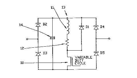
Switching circuitry for use with an autotransfortner for the smooth transition of voltage output from a circuit of either d.c. or a.c.,
between a higher and a lower voltage. The circuit includes at least one, preferably two, variable resistors (13) comprising a first solid state
switch (10), an inductor (11) and a resistor (12), in which the variable resistor (13) is connected to the conductance side of the switch and
wherein the circuit is connected to the voltage ouput of an autotransformer. If the solid state switch used are FETs the variable resistor
(13) is placed within a bridge rectifier (D2-D5). Transition time for movement of the voltage between two levels is approximately one
second.


French Abstract

Circuit de commutation d'autotransformateur, permettant une transition douce de la tension de sortie d'un circuit c.c. ou c.a. entre un niveau haut et un niveau bas. Le circuit comprend au moins un, et de préférence deux, résistances variables (13) comprenant un premier commutateur à semi-conducteurs (10), une bobine d'induction (11) et une résistance (12), la résistance variable (13) étant connectée au côté conductance du commutateur, et le circuit étant connecté à la sortie de tension d'un autotransformateur. Si les commutateurs à semi-conducteurs utilisés sont des FET, la résistance variable (13) est placée à l'intérieur d'un pont redresseur (D2-D5). Le temps nécessaire au passage de la tension entre deux niveaux est d'environ une seconde.

Claims

Note: Claims are shown in the official language in which they were submitted.


THE EMBODIMENTS OF THE INVENTION IN WHICH AN EXCLUSIVE
PROPERTY OR PRIVILEGE IS CLAIMED ARE DEFINED AS FOLLOWS:
1. An electrical switching circuit for smooth
transition between a higher busbar voltage and a lower
busbar voltage (or vice-versa), said circuit comprising:
at least one variable load comprising a first solid state
switch in series with an inductor in series with a
resistor; and one or more second solid state switches;
wherein one said variable load is connected between one
of said busbar voltages and a load circuit and one said
second solid state switch is connected between the other
of said busbar voltages and said load circuit.
2. An electrical switching circuit as claimed in
Claim 1 wherein each said first solid state switch is a
field effect transistor ("FET").
3. An electrical switching circuit as claimed in
Claim 1 wherein one said variable load is connected
between the output tapping of an auto-transformer and the
neutral end of the said auto-transformer and said second
solid state switch is connected between the neutral end
of the said auto-transformer and a neutral busbar.
4. An electrical switching circuit as claimed in
Claim 3 wherein a second variable load is connected
between said neutral end and said neutral busbar, and
wherein a second solid state switch is connected between
said output tapping and said neutral end.
5. An electrical switching circuit as claimed in
Claim 4 wherein said first solid state switch is a field
effect transistor ("FET").

6. An electrical switching circuit as claimed in
Claim 5 wherein said circuit further comprises at least
one diode bridge rectifier when the circuit is used in
a.c. applications.
7. An electrical switching circuit as claimed in
Claim 6 wherein said circuit further comprises one or
more capacitors, one capacitor being placed in parallel
with each variable load.
8. An electrical switching circuit as claimed in
Claim 7 wherein said second switches are selected from
the group consisting of: TRIAC switches, FETs, and
insulated gate bipolar transistors.
9. An electrical switching circuit as claimed in
Claim 8 wherein the transition time for the movement of
voltage output from the circuit from one level to another
is approximately one second.

Description

Note: Descriptions are shown in the official language in which they were submitted.


WO 95/01084 2 1 6 4 8 1 9 PCTINZ94/00060
_
TITLE: SOFT SWITCHING CIRCUITRY
TECHNICAL FIELD
~ The present invention relates to switching circuitry which
permits the gradual, smooth progressive change up or down of the
voltage output of a switching circuit. This prevents any sudden
alteration in the voltage output of control circuitry for
electrical and/or electronic equipment.
BACKGROUND ART
At present when an electrical current is used in one of two
modes (for example, normal mains voltage and a lower than normal
voltage), the switching between one voltage and a second often
needs to be done smoothly and with no noticeable interruption to
current flow.
The problem of smooth switching is particularly relevant when
related to the economic use of fluorescent lights. On start up, for
example, it is important that such lights or lighting systems be
at full voltage. Afterwards however the voltage can be reduced to
reduce power consumption.
Prior art voltage controllers using a single autotransformer
for each phase of a.c. power are known. Examples are shown in
W088/03353 (Econolight Ltd) for non-fluorescent lights; US Patent
No 4219759 (Hirschfeld) for fluorescent lights on three phase
power; US Patent No 4189664 (Hirschfeld) for fluorescent power on
single phase power; and US Patent No 4513224 (Thomas) for
fluorescent lights in which contacts are used to select the
tappings of an autotransformer to reduce the voltage applied to the
lighting load. In DE 3736324 voltage reduction is achieved by
switching a choke in series with the lighting load.
The above ~citations have the disadvantages that there is
either a requirement of critical contactor timing, breakage of the
circuit during switching and no provision for a smooth or gradual
SUE3STITVTE SHEET

~ ~ 548~
change from one voltage to another. With some electrical
equipment (for example fluorescent lights) this produces
a noticeable flicker in the light level, which is
undesirable. For other electrical equipment sudden
changes in voltage are undesirable as they tend to reduce
the working life of the equipment.
An object of an aspect of the present invention is
to provide a switching circuit which permits a ramp
transition between a higher and a lower voltage level
(ramping up and down) of a current, while the circuit is
in operation, which circuits also overcome the
disadvantages of the above prior art circuits. An object
of an aspect of the invention is the provision of such
circuitry for use with either a.c. or d.c. currents.
DISCLOSURE OF INVENTION
The present invention provides in one embodiment
thereof an electrical switching circuit for ramp
transition of the voltage output of said circuit between
a higher and a lower voltage (or vice versa~, said
circuit including: at least one variable resistor
comprising a first solid state switch, an inductor and a
resistor; and one or more second solid state switches;
wherein one said variable resistor is connected to the
conductance ~ide of one said second switch; and wherein
said circuit is connected to the voltage output of an
autotransformer.
Preferably, each said first solid state switch is a
field effect transistor ("FET"). Preferably, if said
circuit is to be used in conjunction with a.c. current,
the circuit includes at least one diode bridge rectifier
of known type. The bridge rectifier is not necessary if

- ~ ~ 648'19
the circuit includes two systems of switching circuitry
in back to back configuration. However more complex
control circuitry than would otherwise be used is then
required.
Preferably, two variable resistors are incorporated
in said circuit. Each said second solid state switch may
be of any known type, for example, a TRIAC switch.
Preferably also a capacitor is placed in parallel with
the or each variable resistor to increasing the smoothing
ability of said circuit.
Where the a.c. circuit includes three phase power, a
circuit as described above and an autotransformer can be
used on each phase.
Another aspect of this invention is as follows:
An electrical switching circuit for smooth
transition between a higher busbar voltage and a lower
busbar voltage (or vice-versa), said circuit comprising:
at least one variable load comprising a first solid state
switch in series with an inductor in series with a
resistor; and one or more second solid state switches;
wherein one said variable load is connected between one
of said busbar voltages and a load circuit and one said
second solid state switch is connected between the other
of said busbar voltages and said load circuit.
BRIEF DESCRIPTION OF THE INVENTION
By way of example only, a preferred embodiment of
the present invention is described in detail with
reference to use of the invention with the variation in
the voltage output of an autotransformer and with
reference to the accompanying drawings, in which:-
Fig. 1 is a circuit according to a first preferred
embodiment of the present invention; and
~'
,~.~

'' -
~ ~ ~48 ~g
Fig. 2 is a circuit according to a second preferred
embodiment of the present invention.
MODE FOR CARRYING OUT THE lN V~N'l'ION
Referring to Fig. 1, a first preferred embodiment of
the present invention is thereshown. A voltage divider
network maintains the secondary w;n~ing of the
autotransformer (not shown) between the high and the low
output modes. The circuit of Fig. 1 includes a FET 10,
an inductor 11 and a resistor 12, which in series form a
variable resistor 13. A capacitor 14 is arrayed in
parallel with the variable resistor 13. Four diodes
(D2-D5) form a bridge rectifier for a.c. current.
The above circuit of Fig. 1 works as follows: the
FET 10 is turned on, and the current through the inductor
11 and resistor 12 slowly builds up. IF the FET 10 i~
then turned off the current will continue to flow through
the inductor 11 and resistor 12 via a diode D1. By
adjusting the duty cycle of the FET 10 the current
through the resistor 12 can be controlled. This variable
current creates the same effect as a variable resistor.
The capacitor 14
3a
,~

wo gS/olo~ 2 1 6 4 8 1 9 PCT~Z94/00060
and resistor 12 also assist in damping out any harmonics generated
within the circuit.
The FET 10 can be switched on and off at a high frequency
with the current smoothed by the operation of the inductor 11 and
capacitor 14. A FET 10 is used in preference to a TRIAC switch (or
- other solid state switch) as it can be switched on and off at much
higher frequencies. ~owever other types of switches can be used,
if so desired. Other types of solid state switches may also be
used, for example insulated gate bipolar transistors (IGBTs). As
the FET 10 can only switch d.c. current, the bridge rectifier is
required.
Referring to Fig. 2 a second preferred embodiment of the
present invention is thereshown. The circuit contains two variable
resistors (as described above) 23, 33 with FETS 20, 30 (and
possible alternatives, as described above), resistors 22, 32 and
inductors 21, 31, respectively). Two bridge rectifiers with four
diodes (D2-D5), as described above, are used in connection with
each variable resistor (23, 33). Capacitors 24, 34 are also used
in the manner described above with reference to capacitor 14. At
point A the current must be controlled, it cannot float. The
current must also be able to flow in both directions.
For switching the voltage output of the autotransformer 40
from a higher to a lower level, the circuit is operated as follows:
variable resistor 23 is switched to the shorted mode (FET 20 is
closed and FET 30 is open). The TRIAC switch 25 is switched off.
Variable resistor 23 ramps down to an off position. At the same
time variable resistor 33 is ramped on and the TRIAC switch 35 is
operated, shorting A to N.
Once the voltage output has been altered, both variable
resistors 23, 33 can be turned off. This leaves the voltage output
at the lower voltage level. The TRIAC switches 25, 35 then carry
the permanent condition of the circuitry. If it is desired to
raise the voltage to the higher level, the above described
SUBSTITI~TE SH~ET

W095tO10~ 2 1 6 4 8 1 9 PCT~Z94/~060
_
operations are reversed.
If so desired, the TRIAC switches 25, 35 may each or both be
replaced with FETs (not shown). These must be placed within the
bridge rectifier for each variable resistor (23, 33) and connected
between the positive and negative terminals of the respective
bridge rectifier.
If so desired, the point E part way along the autotransformer
can be moved to the end of the transformer, at point F.
If so desired, the TRIAC switches described above can be
replaced with any other suitable switch. The inductors 14, 24, 34
may be any appropriate type (high impedance for a.c. current, low
impedance for d.c. current). The size of resistors (12, 22, 32)
used will depend on the power and voltage levels. For example, with
moderate kilowatt power levels and mains voltage of 240 volts, 100
ohm resistors are appropriate. If so desired, any other resistor
capable of handling the power and voltage in the circuit may be
used.
In practice it has been found that a suitable transition time
for the movement of the voltage from one level to the other tin
either direction) is approximately one second. If so desired, this
time can be shorter or longer, depending on the capabilities of the
resistors used.
In both preferred embodiments the order of the positioning
of the inductors (11, 21, 31) and resistors (12, 22, 32) can be
reversed. Other variants of the circuit arrangement are possible.
Equally, the circuit can be configured in manners other than those
shown in Figs. 1 and 2, and still obtain the same functional output
from the circuit.
The first preferred embodiment of the present invention can
be used for control of a d.c. motor. The second preferred
embodiment of the present invention can be used to control any
electrical or electronic devices using a.c. current which, once
switched on, can also operate at a lower voltage. An example of
SUBSTITUTE SHEET

W095/010~ 2 1 6 4 8 1 q
PCT~Z94/0~60
such devices is lights, especially fluorescent lights.
SUBSTITUTE SHEET

Representative Drawing
A single figure which represents the drawing illustrating the invention.
Administrative Status

2024-08-01:As part of the Next Generation Patents (NGP) transition, the Canadian Patents Database (CPD) now contains a more detailed Event History, which replicates the Event Log of our new back-office solution.

Please note that "Inactive:" events refers to events no longer in use in our new back-office solution.

For a clearer understanding of the status of the application/patent presented on this page, the site Disclaimer , as well as the definitions for Patent , Event History , Maintenance Fee  and Payment History  should be consulted.

Event History

Description Date
Inactive: IPC from MCD 2006-03-12
Time Limit for Reversal Expired 2001-06-14
Letter Sent 2000-06-14
Inactive: Entity size changed 1999-06-23
Grant by Issuance 1998-11-10
Inactive: Final fee received 1998-06-17
Pre-grant 1998-06-17
Notice of Allowance is Issued 1997-12-19
Letter Sent 1997-12-19
4 1997-12-19
Notice of Allowance is Issued 1997-12-19
Inactive: Application prosecuted on TS as of Log entry date 1997-12-16
Inactive: Status info is complete as of Log entry date 1997-12-16
Inactive: Approved for allowance (AFA) 1997-12-08
All Requirements for Examination Determined Compliant 1995-12-08
Request for Examination Requirements Determined Compliant 1995-12-08
Application Published (Open to Public Inspection) 1995-01-05

Abandonment History

There is no abandonment history.

Maintenance Fee

The last payment was received on 1998-06-11

Note : If the full payment has not been received on or before the date indicated, a further fee may be required which may be one of the following

  • the reinstatement fee;
  • the late payment fee; or
  • additional fee to reverse deemed expiry.

Patent fees are adjusted on the 1st of January every year. The amounts above are the current amounts if received by December 31 of the current year.
Please refer to the CIPO Patent Fees web page to see all current fee amounts.

Fee History

Fee Type Anniversary Year Due Date Paid Date
MF (application, 3rd anniv.) - standard 03 1997-06-16 1997-06-13
MF (application, 4th anniv.) - standard 04 1998-06-15 1998-06-11
Final fee - standard 1998-06-17
MF (patent, 5th anniv.) - small 1999-06-14 1999-06-14
Owners on Record

Note: Records showing the ownership history in alphabetical order.

Current Owners on Record
SOUTHPOWER LIMITED
Past Owners on Record
DAVID LESLIE LLOYD PEACH
Past Owners that do not appear in the "Owners on Record" listing will appear in other documentation within the application.
Documents

To view selected files, please enter reCAPTCHA code :


To view images, click a link in the Document Description column (Temporarily unavailable). To download the documents, select one or more checkboxes in the first column and then click the "Download Selected in PDF format (Zip Archive)" or the "Download Selected as Single PDF" button.

List of published and non-published patent-specific documents on the CPD .

If you have any difficulty accessing content, you can call the Client Service Centre at 1-866-997-1936 or send them an e-mail at CIPO Client Service Centre.


Document
Description 
Date
(yyyy-mm-dd) 
Number of pages   Size of Image (KB) 
Cover Page 1998-10-25 1 43
Cover Page 1996-05-01 1 15
Abstract 1995-01-04 1 49
Description 1995-01-04 6 244
Claims 1995-01-04 1 45
Drawings 1995-01-04 2 23
Description 1997-11-18 7 256
Claims 1997-11-18 2 56
Representative drawing 1998-10-25 1 5
Commissioner's Notice - Application Found Allowable 1997-12-18 1 165
Maintenance Fee Notice 2000-07-11 1 178
Fees 1998-06-10 1 54
Fees 1997-06-12 1 57
Correspondence 1998-06-16 1 54
Fees 1999-06-13 1 52
Fees 1995-12-07 1 83
Courtesy - Office Letter 1996-03-07 1 29
National entry request 1995-12-07 4 172
Prosecution correspondence 1995-12-07 6 272
International preliminary examination report 1995-12-07 23 660
Prosecution correspondence 1996-12-08 3 93
Examiner Requisition 1997-04-28 2 61
Prosecution correspondence 1997-10-21 2 63
National entry request 1996-03-14 3 114