Note: Descriptions are shown in the official language in which they were submitted.
WO95/28067 21 64833 PCr/US95/04279
MULTI-ZONE LIGHTING CONTROL ~Y~
BACKGROUND OF THE INVENTION
Field of the Invention
The present invention relates to h,l~lo~ in relatively sophictirated
lighting control systemc of the type used most often in colllln~rcial settings for
controlling the l~ ou output of a large number of lighting fix~.;/es which are
grouped together in some manner to define various "zones" of light.
D~ on of Related Prior Art
In many ccllllll~..;ial lighting app1ir^tionc where large lllJ''~ of lighting
fixtures (say, for example, several hundred) are used to illuminate areas of interest,
it is c~.. n to group the fixtures in such a manner as to define "zones" of light
which can be i--~n~ ly controlled from one or more wall~ u~ d control
lS units. The wall-...~ control units are typically located in the vicinity of the
lights they control. Each control unit usually c.)~ s an array of manually
mqnipu1^~.lble zone-hl~ ily or "~1;...... ;.~e" actuators, such as sliders or up/down
push-buttons, each actuator being s~c--;r.r~lly ~ or ~ to a particular
lighting zone. lU~niru1~ion of any one of these a -lUàlGl~ serves to vary a
20 c~ .;t~ lic of a lighting control signal tl ~ -A by the control unit and used to
control the output of one (or more) ~l;..... ;.~g circuits or mnth11es, h~,re;~ el
referred to as ".lhlllll~ ," which apply power to each of the lighting fixtures
defining a particular lighting zone. In addition to providing a meanc for adjusting
the ;..~ n.~ul~s light level of several zones of light, each control unit is usually
25 adapted to store preset values for each of the lighting zones controlled by its
ecliv~ a.;ludlol~. In l~,i,pollse to the ~tn~tion of any one of several "scene-
selectr ~ hes on the control unit, stored preset values can be cim111tqnl~o11c1yrecalled for all of the lighting zones, thereby creating any one of several di~r.,.en
WO 95/28067 2 ~ 6 4 8 3 ~ PCT/US95/04279
lighting scenes in the area ill~ d by the preset lighting zones. Such multi-
zone, multi-scene lighting control units are culllm~lcially available, for example,
from Lutron Electronics Co. Inc. under the l~;i~ d llad~ll,alh "Grafik Eye".
As noted above, it is cc,lllllloll tû locate the lighting control units in the
5 vicinity of the lighting fixtures they control. The ~ . s through which they
control power to the fixtures, ho~ el, are usually mollnted in a centrally located
power cabinet which is remote from the control units and lighting fixtures.
Ct)mm~lnir-q-tion between the control units and the power cabinet has been achieved
by a digital cc,..~ ..ir~ions link in which the control units sequentiqlly ll~.lllil, in
10. a multiplex fashion, zone-illL~ y hlrolllla~ion on a low voltage cC~ ;rqti~nC
bus. The multiplexed hlrullllàlion is decoded in the power cabinet by a
icru~rocessol forming part of a dimmer control panel circuit which controls the
operation of the ~l;...~.. ~. Upon ~eco~ the mllltiplrY~d zone-h~ ily
h~r~ ;on and clet~-...i..i.-g, for example, through an àl,~lù~,ialcly prc,~
15 look-up table, which of the dhlllll~ is to receive and act on certain zone-hll~l~ily
hlrulll~lion lc~;vcd by the "licloprocessor, the dimmer control panel circuit
-~.lllil~ such i~lrul..."irJn to the apprc)p,iàlc dill~ 7. While it is known to
lla~ il this data to the ]i.. - -~ on wires con~ g each dimmer to the dimmercontrol panel circuit, it is also known to multiplex such Ir~ ;OI~ on a digital
20 co------~ ionc link. In the latter case, each dimmer is qccig~d a unique binary
(or digital) address code, and it ~ oll.ls only to zone-hlhl)~ily h~ll,~lion on the
link that is pleceded by (or su,,lehuw ~oc;~tf~d with) its ~e~e~livc address code.
A ll"clul)rocessor q~co ~ d with each dimmer ~JI`OC~-,SeS the address and zone-
h~ .ily i,~ll,ldlion and outputs a d;.. ;.. g control signal which is used to control
25 the firing angle of a triac or the like, thereby adju.,li"g the RMS voltage applied tothe acsociqt~d lighting load and, hence, its lulllilluus output.
In the past, "digital" ~li.. - .~ of the above type have employed either an
array ûf bi-stable "DIP" ~wilclles or one or more multi-positionql rotary selector
swilclles to define the unique address code of each circuit. See, for example, the
digital ~ made by Lite-Touch Inc. In the case of the bi-stable DIP switches, - ~
for example, the binary address code of each dimrner is set during system
in.ct~qll~tion by moving a small switch actuator on each switch of the array to one of
W095/28067 2 1 6 4 8 3 3 PCT/US95/04279
its two stable positions. It will be a~plecia~ed that, in the event that one or more of
the dh~ needs rep!~PmPnt the system user is required to manually set the state
(or position) of the address ~wilcllf;s of the repl~ mPnt dimmer to assure that the
repl~ dimmer responds only to the zone h~ y hlrulll~tion intPntlPd for the
5 dimmer that has been replaced. Should this detail be overlooked or not understood,
a service call may be required to correct the sitn~tion
In addition to the digital addl~ssillg problem noted above, mn1ti7c-nP lighting
systems of the above type are nùloliously difficult to modify (e.g., add dhlllllc;l~ or
change the q~ignmPnt of zone-intensity aclu~lol~) once the system is in~tq.11Pd and
10 opP~ating. It will be ~)lc-~ialed that, during set-up and check-out, written
do~ ion is always available to coll~,lale each dimmer with the zone-intensity
actuator that controls its output. Such ~o.~ ion is usually in the form of a
listing that assigns each dimmer to a particular _one actuator. This listing is
desirable when it comes time to plu~l~ull the dimmer control panel circuit's look-up
table that correlates the individual zone-hll.,.~ily a.,lualol~ with the ~1;.. ~.
Should this clo.~ ;on be unavailable or not readily u~ lood at the time when
morlifir~ti~-n~ or ~ iition~ to the system are r~uiled, a great deal of time can be
e~ ~ in detf---ll;--;n~ what actuator controls what circuit, and what symbology
was used to identify the wne ~ 'ul ~ so that re-prog~ p of the look-up hble
20 can be carried out. Say, for eY~ , a lighting system C~IlllJli_S three wallbox
control units, Ul, U2 and U3, ~ Jose~ at dirr~ t locations within a lighting
region, and each control unit is capable of controlling six lighting zones through the
mqnirU1~tion of six wne-illl~nsiLy acludlol~ Al through A6. Further assume that the
system colll~lise,s 24 ~l;.. :i which control power to the various lighting fixtures
25 of the system. In plogl~llllling the dimmer control panel circuit's look-up hble~ it
is n~ce~ y to assign each zone-hll~l~sily actuator to one or more .1;.","1 .s. To
conseivc~ lloly space, this proglalll,lling is effected by using some abbl~;~ialed
symbology, such as "U2,A3" and "Dl9" to identify a particular zone-hllel~ily
actuator and its q~ignPd dimmer circuit, l~ ,e~;lively. Should one desire to add a
30 new dimmer to the system, one must not only possess the a~alalu~ uhed to
effect re-progl~ll,llillg, but also one must have the knowledge of the symbologyused in plogl~llillg the power panel. Even having this h~....-l;on, the system
Wo 95/28067 2 ~ 6 4 8 ~ ~ PCT/US95/04279
user would then have to know how to p[Ogl~l the power panel, a d~qllnting task for
all but a few. Ideally, the user should be able to add a new dimmer without needfor consultation and/or ~Cs~ nre from the system installer.
A further plobl~ csociqt~d with multi-zone lighting control systems of the
S above type is that of providing an efficient and low-cost means for ~li.cs;~ iug the
sl.bs~ l levels of thermal energy genclaled by each of the I;....... iug circuits so
that a large number of such circuits (e.g., 24) can be housed in a relatively compact
space. As noted above, each ~;~.. i.~g circuit includes a power ~wilchillg device,
e.g., a triac, which serves to hll~.,upl the line voltage applied to a lighting load for
10 a presf~lfec~ed period during each half-cycle to control the RMS voltage across the
load. It also includes a relatively large choke or coil which forms part of a radio
rl~u~ c,r~ .,cf (RFI) su~ ,ssion and lamp de-buzzing n~,.w-,lk. When the
dimmer is optldLing, both of these co...l.o~ heat to Lcnl~.d~u~es well in excessof 100 degrees CPntigra~f~ and act to irradiate the other co"l~on.,.lls of the dimmer
module. To assure proper pc.r..... ~re of the dimmer, it is c~.. ~n to th~rrnqlly
couple the power-swilchillg device and RFI choke to a relatively elabo,dte heat sink,
e.g. an alul,li"ulll plate with heat-d;~;p~ e fins. Further, it is c~....ol- practice to
either select the other dirnmer circuit e~ for their ability to wi~l~l~ld and
operate under high If ll~ alule con~litinn.c7 or to provide sllffiri~nt spacing between
20 the hP~ g~ .dlillg colll~oll~.lls and other ccll~on~ .. As may be a~l~idt-,d,these temperature-c~ e~ ;..g l~.U~is tend to add si&nifi~nt cost to the lightingcontrol system, and/or enlarge the physical size of the ~ ..;ug panel, i.e., thesl~u.;lu~ that SU~U1I~7 multiple ~1;.-..--;..g circuits.
Atl~litionql dla~ack~. of existing digital dhlllll~.~. of the above type are: 1)25 the .J;... ;I~g circuits are not easily by-passed to provide e.ll~.ge.l;~ or ltlll~Olaly
lighting in the event of a loss of the tl;.. i.,g control signal; in such event, jumper
cables are usually used to by-pass or shunt the dimmer and thereby connect the
lighting load directly to the line voltage; 2) their voltage c~ l f .~ -~ ion circuitry is
tailored for dirr~,.f.~L nominal line voltages (e.g., 110 or 277 volts), thereby30 l~uhillg dirr.,.f .l~ dimmer circuits for dirr~ t localities; and 3) they can be
difficult to ~loullc-shoot in the event of system or colll~)on~ failure.
WO 95/28067 2 1 6 4 8 3 3 PCrlUS95/04279
SUMI~ARY OF THE INVENTION
In view of the foregoing discussion, one object of this invention is to
provide a m-llti7On~ lighting control system of the above type in which there is no
need for written doc~ ion in ~c.~igni.~g a zone-h,Lcnsily actuator to a selected5 dimmer.
Another object of this invention is to provide a digital dimmer that requires
no conscious o~ ator involvement in setting its unique binary address code.
Another object of this invention is to provide an improved dimmir~ circuit
panel which, owing to the ~,al~g~ ,nl of the heat-ge.~ i"g collll)on~ of a
10. pluraliity of di~.. ;ng circuits on a specially colll~ul~d metal support plate, is
especi~lly effi~ nt in .li.~ heat, thereby allowing the use of co.lll~ollcllls with
relatively low te.ll~c.alurc ratings, and/or allowing more di..~ g circuits to be
housed in given area.
Another object of this invention is to provide a sirnple means for providing
15 ~hll~Ol~y lighting at a preset level in the event of a loss or absence of a di.,....i.,g
control signal normally used to control the output of a dimmer to a lighting load.
Still another object of this invention is to provide a voltage c~ ion
circuit for stabilizing the lighting system p.,.Ç,lll~nce nolw;l~ ,di~g voltage
variations of a ll~i~.ll nature, such circuit being i..d. ~e ~dPnt of the nominal line
voltage.
A further object of this invention is to provide a low-cost apparatus for
d~ g control unit or dimmer failure in lighting systems of the above type and
for providing a visual indication of such failure to the system user.
Accoldi,lg to one aspect of the invention there is provided an improved
multi-zone lighting control system for sele.,livcly controlling the lc~eclive light
levels of a plurality of lighting zones, each of such zones coll~ ing a dimrnable
light source. According to a pl~fcll~d embo~lim~nt, such lighting control system
C~lllpl b~S:
(a) a lighting control unit for multiplexing zone-hll.,.~ily h~llllalion on a
30 c~ ons link, such zone-intensity h~l"~lion leples~.llillg desired light
levels for each of the plurality of lighting zones, such lighting control unit inrlll-ling
a plurality of manipulatable ~i.. i.~g aclualul~ each being adapted to adjust the
Wo 95/28067 ~ 1 6 4 ~ ~ 3 PCT/US95/04279
zone-intensity h~fu~ ion to reflect a desired change in light level for a dirrcle.
one of the lighting zones; and
(b) fiimming control means up~lalivcly co.-n~ed to the lighting control unit
and l~ ol~iv-e to the multiplexed zone-i.-l-nsily il~lnlalion on the c~ tions
5 link for adjusting the light level of the dimmable light sources to achieve the
desired light level in each of the lighting zones. Plefcl~bly, the ~li.. ,;~ control
means includes:
(i) a plurality of .lhlllll~l~, each being adapted to control the
C output of a light source in one of the lighting zones in ~ ol~ce to
receiving a di.. ;ug control signal; and
(ii) means for qCcigning each of the 1;.. ~ .. to a particular dimming
actuator so that the ~ei.~-~livc input signal Iccei~ by an ~ dimmer is
d~ by the zone-hl~,nsily hlrullll8lion adjusted by such particular ~ ...n;~g
actuator, such q~cigning means CO1l4J~ illg: (1) means for s-~lPrl;.-~ a particular
15 dimmer, and (2) means l~Ol~i~.., to a plc~et~-.u;..-~ se.l.l n~e of changes of zone-
hltcl~ily h~l... ~inn on the co.. ~ .irqtifJnc link as plol~,_ed by a pre~ t~ .",;n
mqnipul~ion of any one of the fl;~ ";.~g aclu~tu~s to assign such one ~I;.. ;.,g
actuator to the selected dimmer.
Accoldhlg to a second aspect of this invention, there is provided a self-
20 addl.,s~illg dimmer that is adapted for use in a digital lighting control system of the
type CfJlll~li;,illg a central control unit which c".. ~ cs with a plurality of such
fl;~ over a culllllloll co,.. ~. r ~ionc link to control the power applied to a
plurality of lighting loads. Each of the ~li.. f~ coll4,1i~es (i) a housing (e.g. a
circuit board) adapted to be llwulllcd in a pre~lct~,....i..-~d location on a support plate,
25 and (ii) means for storing a unique binary address code by which the central control
unit can co.. ~.;r^te exclusively with any one of the li,.. ~ . over the c~ lllon
co.. ~ ion~ link. Preferably, the address code-storing means Cflll~ fs a
plurality of electrical switches mounted on the a~oci~tf d housing of each dimmer,
each of such ~wilches having means for controlling the conductive state (open or30 closed) of its ~o~ contacts. Accoldhlg to this aspect of the invention, the
state-controlling means of each switch is controllable by switchcontrolling means
di~osc~ on the support plate. Thus, as the dimmer is IIIU''lItf-tl on the support plate
Wo 9S/28067 2 1 6 4 8 3 3 PCrtUS95tO4279
in its proper position, the switch-controlling means on the support plate cooperates
with the state-controlling means on the dimmer housing to selectively and
ql~tnmq~irqlly set the ,e~e~;live conductive states of the ~wilchcs, thereby setting the
address of the dimmer. Preferably, the state-controlling means of each switch is in
5 the form of a push button or plunger-type switch actuator which is spring-biased
toward an outwardly ~trn-ling position, and the switch-controlling means on the
support plate CO~ l;S~S an array of holes and lands in the support plate. When adimmer is plopc-ly ml l-ntrli on the support plate, the lands interact with selected
switch acluàLo,~, causing them to move from their ,~ ecLive biased positions to
10 their non-biased positions. I~Ieallwhile, the holes allow the r~ g switch
acLuaLol~ to rernain in their resl,ecLivc biased positions. When â single support plate
is used to support multiple dillllll~ , the support plate is provided with multiple
unique hole and land patterns o~ iLe each location that is intrnllrd to support a
dimmer. Thus, the address of each dimmer is ~le~ d by its position on the
15 support plate.
Accordillg to a third aspect of this invention, there is provided an i ll~ ved
~li..... ;.~g panel which inrl~ldes a thrrmqlly CO~ J~I;VC support plate and a plurality
of ~I;..... ;.,g circuits each having a heat-producing power swile,l~ing device and a
choke. Acco~lhlg to a pref~,.lcd Pmhorlim~nt the support plate has a corrugated
20 cross sec~iol, and the ~w~ecli~ chokes of the .l;-.-...;.,g circuits are ,...~ ,t~i in
close pluAhllily to each other on the support plate at a locatiûn remote from their
qccor;~.~i .l;.. ;.~g circuits. This has the effect of ~b~ lly lowering the
arnbient t~ dlUlC in the vicinity of the other circuit Cul~pO~ ;, thereby
prolonging their lespe~livc lifrtimrs.
Accolding to a fourth aspect of this invention, there is provided a h.ll~
lighting feature by which a preset lighting level can be provided in the event there is
a loss or absence of the control signal used to control the output of the digital light
Accoldhlg to this aspect of the invention, means are provided for (a)
sensing the absence of the control signal; (b) switching power OFF and ON to the 30 dilll,ll~,r. and (c) ~l~tecting the occull.,.lce of both (a) and (h) and, in response
thereto, applying a pred~ t~ f~ g level control signal to a control circuit
adapted to control, e.g., through a triac, the current flow through a lighting load to
WO 95/28067 2 1 6 4 8 3 3 PCT/US95/04279
selectively adjust the lul~ ~us output thereof.
According to a fifth aspect of this invention, there is provided an improved
voltage CO~ )c;llSaliOll a~)dlalllS which is adapted for use in a light dimmer for
,.,~i..l~;.,;l.g a sl-bst~nti~lly cor..cl~..l Ioad current nolwil~ ing short-lived changes
S in the line voltage. The a~l,a,~lus is useful with any conventional A.C. Iine voltage
source (e.g. 100, 120, 220 or 277 volts, 50 or 60 hertz) and pl~f,~ably co",~,iscs:
(a) means operatively con,,c~lcd to the A.C. voltage source for dP~ g
a first time interval ~ ce~ g the average time ,~.luir~ for the A.C. waveform toreach a pre~leterrnin~d threshold level during each half cycle of a nominal operating
10 period;
(b) means opelalively con..P~led to the A.C. power source for dele ..~ g
during each half cycle of the waveform a second time interval r~res~i.,li"g the time
~uilcd for the A.C. waveform to reach such pl~,t' ..~ d threshold level;
(c) means for c~ the first and second time intervals during each
15 cycle of the waveform and for producing an error signal lep.es~.lling the dirr~.ellcc
in such time intervals; and
(d) means for adjusting the firing angle of a triac or the like used to control
the power applied to the lighting load accordi,lg to the value of the error signal to
the RMS voltage across the lighting load at a ~ Ily constant level
20 nclwi~ ;ug short-lived ~alialiolls in the a",~lilude of the A.C. waveform of the
voltage source.
Accol.lh,g to a sixth aspect of this invention, there is provided a diagnostic
a~aldlus adapted for use in a light dirnmer of the type which scle~liv~ly controls
the current flow through a lighting load to adjust the ll..,.;.,....c output thereof, such
25 light dimmer colll~ illg (i) a controllably coluluctive device (e.g. a triac)col...~c~ c in series between an A.C. power source and a lighting load, and (ii) a
control circuit which resl)ollds to a ~l;....,.;..g level control signal provided by a
lighting control unit to sele~,lively apply a selected portion of an A.C. voltage
~.avcfOllll produced by the A.C. power source to the lighting load to adjust the30 RMS voltage across the lighting load, such selected portion being d~ .Pd by aphase angle at which the control circuit causes the controllably con~ rtive device to
conduct power during each half cycle of the A.C. wav~r~?llll. Accoldillg to this
Wo 9S/28067 2 1 6 4 8 3 3 PCT/US95104279
aspect of the invention the 1i~n~stic a~a,~lus coln~lises
(a) means for sensing the ope,~li"g status of a colll~ol~llt of the dimmer
and/or the pl~,ence of the ~imming level control signal;
(b) logic and control means for co p~; g an output of the sensing means
S int~ ting the present c,~e.~li"g status of the cc",l~ullenl and/or the prcs~ l,ce of the
g level control signal with a stored value; and
(c) a status indicator prefelably a single light ell,i.lhlg diode, which
1~ ~pollds to an output of the logic and control means to provide a visual infli~tion
of a change in status of the co,ll~olle.ll and/or the p,esence of the control signal
The invention and its various aspects will be better ulld~.Dlood from the
ensuing detailed description of pl~;rell~ embo~lim~ntc I~Ç. .~ .Ice being made to the
. ~- .yillg ~llawill~D
BRIEF DESCRIPIION OF THE DRAVVINGS
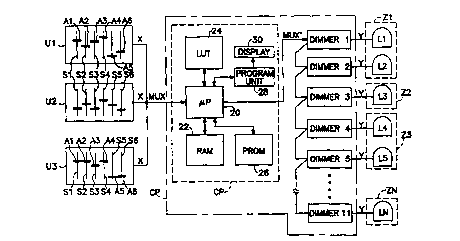
FIG. 1 is a block (liagra n of a multi-zone lighting control system of the type
in which the inventions disclosed herein are useful;
FIG 2 is a more detailed block diagram of the dirnmer control panel of the
FIG 1 system;
FIG 3 is a front plan view of an hll, l~;livc display panel useful in
p~u~;~An~n;~-~ the programmable dimmer control panel of the FIG 1 system;
FIGS 4A and 4B are flow charts of a CO~ plO~l~ull adapted for use in
the FIG 1 system for ~C~igning a desired zone-hltw,Dily actuator to a selected
dh,~lel,
FIG S is a block diagram of a digital dimmer elllbo~illg various aspects of
the invention;
FIG 6 is a peral,ecli~e view of a portion of a support plate adapted to
support a plurality of the dhlllllela;
FIG 7 is a pr ~l,e~ivc: view of a ~limming panel illllctra~ing a plef~ llcd
layout of ~limming circuits and chokes;
FIG 8 is an end view of a portion of the dimmer panel shown in FIG 7;
FIGS 9-11 are flow charts ill ~l ~; g various plOrlallla carried out by the
~icl~rocessor cullllJonelll of the dimmer shown in FIG 5; and
W O 95/28067 2 1 6 4 8 3 3 PCT~US95/04279
- 10-
FIG. 12 is an electrical 5~h .~-lic showing pl~,f~.led ch-;ui~l.y for
implern~nting various aspects of this invention.
DETAILED DESCRIPTION OF PREFERRED EMBODIMENTS
S Referring now to the dlawill~;s, FIG. 1 s~h~ lly illustrates a multi-zonelighting control system in which a plurality of lighting control units U1, U2, U3
operate through a plurality of dhl~ (dimmer 1 through dimmer N) to control the
output hlLèl~i~y of a plurality of lighting loads L1 through LN. While each of the
lighting loads is scl.~ lly depicted as COlll~ i lg a single fixture, it will bea~~ idt~d that each lighting load usually col,l~,lises several, and often many,
individual lamps of the same type, e.g., all being either j~r~l)rlr.~ t fluorescent,
neon, etc. As shown, the lighting loads may be grouped tGg~lhcl to define a
plurality of lighting zones Z1, Z2, Z3, ... ZN, the light h~ y of each zone being
controlled by the output of one or more of the dhlull~. In the FIG. 1 system,
15 control units Ul - U3 are of col,~e.llional design, each colll~ ing a plurality of
zone-h,l.,.~iiy a~,lu~ol~ A1 -A6, shown as sliders, which can be manually
manipulated, such as raised or lowered within slots S1-S6, r~e~ ely, to vary a
cl,a,acl~ lic of a lighting control signal pr~luced at the output x of each unit. As
explained below, the le;",ecli~/e outputs of the control units serve to control the
20 le~li~re outputs Y of the rl;-----.;ne mr-~lulPc and, hence, the light hll.,.~ily of the
lighting zones. Each of the actuators Al - A6 controls one or more dillull~ to
control the light hll~ ily in a particular lighting zone to which the rli.,"". :, are
~si~-~, e.g. actuator Al of control unit Ul may control the lighting i"l~.~ily in
zone Zl by controlling the outputs of diulun.,l~ 1 and 2; actuator Al of control unit
25 U2 may be ~cign-~ to control the output of dimmer 3 which controls the lighting
hll~,nsily in zone Z2; and actuator A4 of control unit U3 may be ~c~ign~d to
dhlull~ 4 and 5 which control the lighting hllel~ily in zone Z3. In the control
units shown, physically moving the slide actuator in the slot acts to raise or lower
the light level. In some control units, hc ~ ,l, the zone-h-lensily actuator may take
30 the form of a pair of UP/DOWN push buttons which, through suitable circuitry,have the same effect on the control unit output. Suitable control units for the FIG.
1 system are the so-called Grafik Eye T ightirlg Controls, Models 3000 or 4000,
WO 95128067 2 1 6 4 8 3 3 PCT/US95/04279
made by Lutron Electronics Co., Inc.
~ .ighting control units U1 - U3 are usually wall-mounted devices, each beingw-led in a wallbox located in the vicinity of the lighting fixtures they control.
The control units c~ ;r~te with the various d;..... .;~-g modules through a
5 progla"..l able dimmer control panel circuit CP which, together with tne ~limming
modules, is housed in a power cabinet PC located remote from the controls and
lighting fixtures, e.g. in a power control room . The dimmer control panel circuit
in~ludPs a miclùplocessor 20, such as a Motorola Model 68HC11E9, eight-bit
l. icloco..l.oller, which receives multiplexed zone-i..l~.~ily h fu~ll alion l.~ Pd
10 by the control units over a digital c~ ir~ations link MUX. Upon being
se.lu~ ly polled in a collvrlllional manner, each control unit lla~ , in
accoldance with an established protocol, a serial message on the link, such -Rssage
l~UleSC-Il;l~g digitally enro~P~ zone-intensity h full~lion dr~ d by the position
of its six zone acludlol~. Polling of the control units is typically effected at a
15 relatively fast rate, e.g., once every 100 ms., each control unit taking its turn in a
p~ r..~ time-slot. Upon ec.,;vi-.g and de-mllltirlPYin~ the zone h~ bily
h ru~ll alion from the lighting control units, the ll~cropl(~cessol stores this
i~ fc ....~;on in a conve.llional random access Ill~,lloly (RAM) 22, ~ ;.lg the
Ill~lllUly with fresh hlt~ ily i-lrulll alion during every poling cycle. As shown in
20 FIG. 2 which i~ ctra~rs certain plef,l-~ details of the ~I;.. ;.,g control pane
circuitl, the zone-i-~ ily hlfulll~lion is stored in tabular form, each box (e.g., U1,
A1, which ille-~;r.es actuator A1 of control unit U1) CQI~ lg eight bits of zone-
hll~ ily h-rulll~ion for the ~o~ zone actuator for the precelil.g polling cycle.In the system d~;cl~d in FIG. 1, there are a total of eigh~n zone actuators; hence,
25 RAM 22 must .~cch~....n~l~te eighte~n hlt~,nsily levels, one for each actuator.
Still l,,f~,llhlg to FIGS. 1 and 2, the .1; ;.. ~ control panel circuit further
colll~.ises a look-up table (LUT) 24, pref~ldbly a sl~ldard electrically erasable read-
only ~e.~uly (EEPROM ); a pro~l~..ll.able read-only ..-~..-o.y (PROM) 26
(described in conci~lerable detail below); and a plOgl~lllllillg unit 28 inrlu~iing an
30 hll~la--liv~ display 30 through which the look-up table can be progla l--l-ed to assign
each d;.. ;.,g module to a particular zone actuator. While shown s~;~âlàl~ly, it will
be al"u.~.,ia~ed that the look-up table and PROM are often integral portions of the
WO 95/28067 2 1 6 4 8 3 ~ PCrlUS95/04279
microprocessor and, in fact, are part of the Motorola miclocolllloller mentionedabove. In the example shown in FIG. 1, it is shown that dillllllt;lo 1 and 2 control
the lamps in lighting zone Z1. Thel~Çole, in setting up the lighting system, it is
nPces.c~,y to assign .lillllllc;lo 1 and 2 to a single zone actuator, and to store that
5 ~Csignmpnt in the look-up table. As shown in FIG. 2, dh~ o 1 and 2 have been
~Csignpd to zone actuator Ul,A1, i.e. actuator A1 of control unit U1. This
~Csig~mpnt is normally achieved by ~p~loplialely pro~;l~ll.lnng LUT 24 through the
plOglall..llillg unit 28. Similarly, FIG. 1 shows that tlimmir~ module 3 controls the
lamps of zone Z2. In FIG.2, it is shown that the look-up table has been
10. plog~ lled to assign actuator Ul,A2 to this particular lighting zone. Further, it is
shown in FIG. 1 that dhl.lll.,lo 4 and 5 control the larnps in zone Z3. Referring to
FIG. 2, control of these dhlllll~,~o has been ~c;g,~ in the look-up table to zone
- actuator U1,A3.
Referring to FIG. 3, the prog..~ g unit 28 includes an hl~.acliv-e display
15 30 which is illustrated as CullllJl;sillg a pair of seven-segmpnt LED (light-e,. iuing
diodes) displays 32,34; a series of push-button O~ ,hes 35 - 39; and an array ofsingle LEDS 40 - 45. Display 32 is part of the "Select Circuit" portion of the
plOg~ display and is adapted to show a number r~res~.lli,lg a particular
.l;,",,,i,~ circuit number. A desired ~;~.. ;.~g circuit number is selected by
r~c~t~ly d~lcssillg the dpplo~ e UP/DOWN buttons 35,36 until the display 32
shows the desired circuit number. ~ of the selected circuit to a particular
zone actuator is ~chi~ d in the "Select Value" portion of display 30.
Upon sP~ the desired dimmer and C.lt~,~illg a plogl~ll mode (e.g., by
depl.,ssh.g buttons 35 and 39 cimn~ F~ ly for a pred~ ...;..Fd time period),
button 39 is repeatedly dep~Osed, thereby causing the LED's 40 - 45 to become
ill.. ;.. ~, one at a time. These LED's .eO~e~;lively identify various internal
plogl~lls that are stored in PROM 26, each plOgl~lll enabling the user to adjustcertain dimmer paldlllet,~o and store certain values. When LED 40 is il~ uled~
for example, a program is ~ccPsced which allows the user to chose one of four
dirr~,cl~l load types (i.e. in~n-lPcc~Pnt or low voltage, fluorescent, neon or cold - ~
cathode, or non-dimmable) by d~OOing the UP/DOWN buttons 37,38 until the
number (from 01 to 04) is shown on display 34. Based on the load type chosen, the
Wo 95/28067 2 1 6 4 ~ 3 3 PCr/US95/04279
- 13 -
prog.~l,l, ing unit causes the micloprocessor 20 to l.~.",L a load-type signal to the
selected dimming module, causing the rlimming module to chose an a~rop-i~le
calibration curve (stored in Ill~,.llUly of the .I;... ;I~g module) for ~i.. i,-g the lamps
controlled thereby. When LED's 43 or 44 are ill~ eA p108~ S are accçcced
5 which allow the user to set either the lowest or highest intensity level available for
the selected dimmer. When LED 41 is illl....;..~trd, the opcl..tor can assign a
desired zone actuator to the selected dimmer through the i.~l~"acli-~e display. At this
time, the seven-segm~nt display 34 ~Itern~tely displays, for one second intervals, a
particular control unit number, e.g. U1, and a particular actuator number, e.g., A1.
10 By d~-essing the UP/DOWN buttons 37, 38 at the ap~,ru~.idle time, the operator
can i-,e,c.,.e.,l the displayed number by one and thereby select a desired control unit
and zone actuator. Having selected both the ~I;....... ;.~g circuit number and actuator
number, the "~icrop,ocessor assigns (or re-assigns) this particular actuator to the
selected ~ ;ug circuit after a preset time interval has elapsed, and stores this15 ~c~ignmrnt in the look-up table LUT 24 .
As may be a~,u,ccialed, ~c.cignjng a particular zone actuator to a dimmer in
the manner dr3~ - ;I-ecl above requires knowledge by the P1~ - . of the actuatorsymbology. At initial set-up of the system, there is always some doc~ fion~
e.g., a work sheet, that correlates these two variables, control unit number and20 actuator number, in a symbology lln~4rctood by the ~ucro~,uc~ .or. With the
passage of time, hc,.._~,., such do.;~ 'ir,n often .li .l.~,e~.~., and even the
smallest change in actuator ~c~ig"".. ,I~, or the ad~lition of a new circuit to the
system, often requires a service call to the system installer who prc~.ul~ldbly has
retained the nrce;~r~ cloc~ ion to make a change.
According to a one aspect of this invention, the above-noted difficulty in
making motlifir~tions to an existing lighting system of the type described is
alleviated by the provision of a CO~ ul.,. p.u~;.~-, that obviates the need for any
do.~ ion in order to re-prog,a", the look-up table 24 with new zone actuator
~Signmf~ntc. Accoldillg to a pref~,.,~ ~;llll~,o~ ..- .1, this p,roglall" which is stored
- 30 in PROM 26, causes the a~aldlu~ to carry out the se.~vc~e of steps shown in the
flow chart of FIG. 4. Upon entering a prc,~ ""i"g mode as desc,ibed above,
l.. lloll 39 is ~ c~ Aly d~lessed until LED 42 is ill.. ;~ ed This LED
WO 9S/28067 2 ~ ~ 4 8 ~ ~ PCT/US95/04279
- 14-
in~ qtçs that the "Zone Capture" program has been qcce~ed The operator then
selects a '~ ;"E circuit for zone actuator a~signmPnt by dc~ ,ssillg UP/DOWN
buttons 35,36. Having made the circuit selection, the microprocessor outputs a
signal to the selected dimmer, causing the lamps on the selected circuit to lcpcd~cdly
5 flash, full ON and OFF. This flashing is intton~lP~ to give the op~.~tor a visual
indication of the lights controlled by the selected di..-...;.-g circuit. The u~latol
then goes to the specific actuator which is ;. Ir~ pd to be a~ienP~ to the selected
~1;.. ;.~ circuit and physically moves or manipulates the actuator so as to request a
...;~,;...~.. light level. In the control shown in FIG. 1, the opel~tol would move the
10 slider to the bottom of its ~ c~;livc slot. Upon d~ te~ that any of values stored
in RAM 22 are at the ...;.~ .. allowed level, the micr~loccssor sets a binary bit
or flag. Having manipulated an actuator to request ~ Iight level, the
operator is then r~uirc~ to mqnipul^~ç the actuator towards a position requesti~...~x;... --.. light i~ ily, e.g. moving the slider towards the top of the slot. At this
15 time, the lllicloprocessol starts an internal timer which sets a time period (e.g. 5
seconds) during which the next seq~ e of events must be completed in order to
assign the mqnirll^~ed actuator to the selected .l;.."..;.~ circuit. The opeldlor then
continl~P~ a~ju~l;ug the slider towards a position l.~ f;,l;.~g ...~ .. Iight level.
During this time, the lllicluplocessol lllonilol~ the illt~ y values of the zones for
20 which a flag was set at the be~ ;u~ of the timing period. As soon as one of the
zones, pl~i.-,lllably the zone whose actuator is being a~liu~te~ reaches a
e~ ";~r~ value, say, 50% of .. ~xi.. , value, the microl,lucessor causes thelight illt._.~ily of the lamps on the selected dimmer circuit to stop flashing and track
(in illltn.sily) the ~ 1 or lllo~lllclll of the actuator. At this point, the selected
25 dLmmer has now been "cà~lul~d" by the actuator. Upon noticing that the lamp(s)
on the c~luled dimmer are tracking the actuator adj~ , the ope.àtor begins to
adjust the zone actuator in such a manner as to again request ...i.i;...~... (e.g. zero)
light hll~,.lsily. If the actuator has arrived at the ..i..i..~ .. Iight level setting before
the internal timer times-out, the selected dimmer will be "locked" to the adjusted
actuator, i.e. the lllicl.,processor will re-progldlll the look-up table so as to assign - ~
the ~ t~A actuator to the selected dim- mer. If the internal timer times-out
before the actuator arrives at the ...i..;...~.. light level setting, the plO~lalll returns to
WO 95/28067 2 1 6 4 ~ 3 3 PCr/US95/04279
the dimmer-selection step, and the q-c-sociqted lamps on the selected dimmer begin to
flash ON/OFF again.
By virtue of the above al)lJâldlus, it will be a~ .,iattd that a user can re-
configure an entire lighting system, i.e., re-assign any or all of the acludtol~ to
5 dirre~e~.l dh~ , without ever having any knowledge of the symbology used in
initially progld,.llllhlg the system. Similarly, di~ can be added to existing
zones, or qccignPd to previously nnq~ignpd aclualol~ without knowledge of the
actuator "llUllll~
Referring to FIG. 5, there is shown a filnrtionql block diagram of each of
lû the .1;,.~ . d;C~ s~d above. The general purpose of each dirnmer is to provide a
phase control output to its qCSori~pd lighting load LL to control the RMS voltage
across the load and, hence, its ll....;.~ c in~ ily. As ~i;c~ sed below, each
dimmer is adapted to operate on a wide range of input voltages from 80 VAC to
277 VAC, 50 or 60 Hz. A circuit breaker CB fimrtion.~ in a coll~e.llional manner15 to provide AC o~ ,ull~.ll plot~lioll. It also funrtil~nc as a means for removing
power to a dimmer, each dimmer having its own breaker. A relay R serves to
break power to the load and O~ates under the control of a llliclul)loc~i.sol MP.The ~wilched power of the relay serves to provide power directly to a controllably
con~lctive device, pll,fe~ably a triac T, and it can also be used to provide a
20 swil~,hcd hot output ~rC~cc~ for ~ ....;ng lluoles~.l~ Ioads. The ll.,cloplocesso
controls the turn on se~ .re of the relay and triac so that the relay contacts are
closed with no current through them. The triac l~lJUI~ds to a control signal on its
gate lead to selec~ ly conduct a portion of the AC line voltage during each halfcycle thereof, whe.~y the RMS voltage across the load can be varied. The triac's25 ON time is controlled by the llli.;luplocessor and is based on the digital values
received on the c~ ;rq-tions link MUX' from the control ~ igl~rd thereto. As
$~ below, a plurality of address swi~ s provide each dimmer on the
c~ ion~ link a unique address so that each dimmer can identify zone
~ tllSily il~llll ~io~ int~ntl~ for it.
Each .I;,,.. ;.~g circuit also includes a full wave bridge circuit FWB which
rectifies the AC line voltage to provide the DC voltage needed to operate the
llliclu~rocessol and relay coil. A power supply PS uses the rectified AC line
WO 95/28067 2 1 6 4 8 3 3 PCr/US95/04279
- 16-
voltage to provide 30 volts DC to operate the relay. The power supply also derives
a regulated 5 VDC supply to power the micloprocesso~. A zero-cross detector ZC
senses when the line voltage ~.a~.,ro,ll, crosses zero and provides an input to the
llliclui)rocessol for cl;;l~-...;..;,~g the line fl~u~ r and phase. A voltage
5 c~..l.l..n~ion circuit, ~Iic~-u~~ced below, operates to ~ A;~ a constant light intensity
even when the AC line voltage n~ es from its nominal value. As also ~licc~sced
below, the micloprocessor is prû~lalllllled to respond to various inputs, inr.h--ling a
triac fault detector FD, to indicate the OpC.a~ g status of the system and various
key culllluo~ . Such status is ;..~1;r~ed by a causing status hldic~lor SI,
10 plerelably a single LED or other light source, to flash accor.li,lg to a pre~el~ f ~
se~ re. A large choke C (e.g. up to 2 or 3 millihPnry) is CO~...f ~:~ in series with
the triac output and serves to ~ .S RFI and reduce lamp buzzing in inr~n~PscPnt
lamps.
In the lighting control system d~lil,ed above, it is noted that the tlimmir~
control panel circuit CP controls the ,~e~ , outputs of the ~l;.. ~ (Dimmerl -
Dimmer N in FIG. 1). Pl~,f~,,,.bly, c~ ;nn between the control panel circuit
and dimmer circuits is carried out on a two-wire serial data link MUX' to which the
dilll,ll.,,~ are c~ l~ in a daisy-chain fashion. So that each dimmer ~..,uol~ds only
to hl~ y hlrulllld~ion ;.~ ed for it, each dimmer is c~"".--ol-ly ''~ r~ a
20 dirf,.e.ll binary or digital address. In prior art systems, such ad~wsillg has been
a~ .~ either by an array of bi-stable "DIP" ~ ,hes, each having an actuator that can be moved between two stable positions, or a rotary, multiposition~l selectorswitch which, based on the position of a ru~tàbl~ selector el~mPnt df~ s thedimmer address. In the event a dimmer requires l~ .l it will be appreciated
25 that the new unit must have the same address as the defective unit. This requires
some attention to detail by the servicing p~.~u~lllel in that an unobsG,~ed ~eidPn
.~.ll.,lll of one of the switch a~;luà~ul~ on the DIP switch array, or a rotation of
the selector element of the defective unit prior to setting the address of the new unit
can be problematic in setting the address of the new unit. Ideally, the repl~rPmPnt
30 dimmer should be self-addressing so as to elimin~tp human involvement in the
addleishlg process.
Accor.lillg to a second aspect of this invention, there is provided a digital
Wo 95/28067 2 1 6 4 8 3 3 PCr/US95/04279
dimmer that ~ o..,~ qlly addresses itself as it is mount.od on a support plate. The
features which enable it to be self-addl~,sshlg are better shown in FIG. 6. As
shown, each dimmer module, designqtF~i as Icr~ ce chalacl~,r 50, co",~lises a
housing 52, e.g., a circuit board, which is ll,oullLable in a prede~e...,il-Fd location L'
5 (shown in phalllulll lines in FIG. 6) on a support plate SP. The dimmer circuit
board ~U~J~Ull~i the various clF~llunic Colll~Jol~,ll~ iscnssed below with l~,f"ellce to
FIG. 12) l~uired to vary the intensity of a lighting load in le;",ollse to reccivillg a
suitable lighting control signal. As noted above, such colll~oll~,,ll~ include a triac T
which is used to sFlF~ively hlL~ l,uL power to the load to dim its output.
10 Accoldillg to a pr,,f~ ,d c.llbodilll.,.lL, each dimmer module 50 has a unique binary
address code l1~ t~ i by an array of normally open address swiLches 56 - 60,
located at the pc.i~l~le,,y of the circuit board, and means qCcociq~d with the support
plate for selF~;Livc;ly ~ g the con.~ e state of one or more of the ~wilches as
the dimmer module is IllUII"I~i in a pre~1cl~-...;..f~i location~L' on the support plate.
15 ~cr~,ably, each of the swilchcs is of the type which includes a Illovdl)le plunger P
which, d~pen~ on its eYt~n~l~ or ~llact~ position, d~ t~ ...;..~s the conductive(open or closed) state of its associated switch. Normally, the plunger of such
Swill,ll S iS spring-biased towards its c~ i position, in which case the switch is
normally open. ~f."l-,d address ~wil~_llFcs are the "Detector Switches," made by20 r~ lsl.;l;. EIe~;I1U1LCS C~ FnI~ CO. When address ~.iL,Les of this type are
used, the switch-closing means on the support plate may take the form of an array A
of holes H having lands L Lh~,r~cL~.~" and on o~o~iLe sides thereof. When the
dimmer module is prop~,ly position~l on the support plate, the holes act to allow
some of the plungers to remain in their normally c~ ed position, thereby allowing
25 their rc~l,e~Li./e swiLches to remain open, while the lands act to selec~ ly depress
the 1~ ;--;ug switch plungers, thereby closing their rei,l.ecLive swiLchcs. Thus, it
will be a~lcciàted that the dimmer's address is d~t~-...;n~d by the hole/land pattern
opposite the position in which it is IlluunLcd. By using dirr~ hole/land patterns,
each dimmer module can receive a unique binary address code. ~cr~"ably, a
- 30 plurality of I;~ g m--rhll-os are IlloullL~,d on the same support plate and, opposite
each position on the plate which is to receive a dimmer module, a dirr~". ,
hole/land pattern is formed.
WO 9S/28067 2 1 6 4 8 ~ ~ PCr/US95/04279
In the self-addlessing scheme described above, each of the address ~wilches
includes a pair of contacts which are shown in the electrical sr~ ;c of FIG. 12.One contact of each pair is co~ e.;led to a voltage source. In response to switch
closure, a signal appears at the switch output. The rc;.pec~ e outputs of the address
5 switches serve as High/Low inputs to a microprocessor forming part of the dimmer.
Prior to acc~ h~g illtensily hlrol,l.alion from the dimmer control panel over the
multiplex link, the binary address produceA by the address ~wild~es must match the
address llA~ rA on the serial data link.
In the prc;Ç~"l~ embodiment shown in FIG. 6, there are a total of five
10 address ~wilches 56-60 which define a five-bit binary address code. Obviously, the
number of ~wil-;hes is cl(t. -.. ;.. rli by the ~ .. number of ~;~.. - .~ alloweA on
the cc.. ~ fion~ link. As noted, the dhl.. ~.~ have predefin~ g
locations on the support plate, each of such locations being ~l~t~-...;..~i by a pair of
spaceA guides 62 which engage the lateral edges of a module's circuit board. Each
guide is provideA with ol,~osillg grooves so that ~ jaGent circuit boards can share the
same guide. Each guide is provideA with a pair of I'IIJII~ g clips 63 which are
~le~ign~i to snap into e-~g~g,..- .l with a~ ;s 64 formed in the support plate.When the ...~)v~ g clips are po~ifion~i within the d~ Ul~S 64, a pair of feet 65 on
each guide engage the support plate surface at locations 66. When so position~
guides 62 serve to postion the circuit board upright (pc~ irll1qr) with respect to
the support plate surface.
While the above embodiment uses an array of ele~;lr~ rrh~n;~Al ~wil-;hes
and support plate holes and lands to provide the self-addressing feature, other self-
addressing sr~ P~ come to mind. For example, ma~n-otir address switches can be
used which co~ with a m~nPfir/non-magn~tir pattern on the support plate.
Alternatively, photo&lGctric swilcll~s can be useA which cooperate with a
reflectivelnon-reflective pattern on the support plate.
Referring now to FIGS. 7 and 8, another aspect of this invention relates to
the dimmer support plate and the al-~lgenl~lll of the heat-g~ g dimmer
30 C~J111~OI1~ thereon to achieve a relatively high packing density of dimmer modules.
As noted earlier, each dimmer includes, in addition to a triac or the like, a
relatively large choke or coil for ~ hlg RFI. When the dimmer is op~-dhlg,
Wo 95/28067 2 1 6 4 8 3 3 PCT/US95/04279
- 19 -
both of these components generate so much heat that it is c- In,,lùn to provide some
sort of heat sink for CC?Il~lU~ g heat away from the other circuit elPmPntc to avoid
damage or, at least, prolong their useful life. Often, a number of fli.,.. ~COlllpli~illg a flimming panel are s,l~olled on a cùul.,noll, heat-conflurting, support
5 plate with the hP~ gellelalillg colll~oll.,.ll~ of each dimmer being thPrmqlly coupled
to the plate. Usually, the support plate is a casting or extrusion having a plurality
of fins or ribs on the o~luosil~ side thereof for l~idlh~g the heat con~ c~tP~d thereto
into the ~ ùundillg air. Ideally, the RFI choke, being the larger produc_r of
thermal energy, should be remotely spaced from its P~coci~t~ dimmer components,
10 but since cullv-e,llional din..nel~ are packaged with the choke included, the choke is
usually positioned relatively close to its Pccoci~pd circuit co...pon~,..l~.
As an qlt~Prnqtive to using relatively costly castings or extrusion of fiMed
surfaces and the like, and to mounting the choke-co.. ~ g I;....... .- ~ side-by-side on
a flat, heat-co~ c~ g support plate, it is plef~.l~ that the support plate take the
15 form of a corrugated metal sllu.;lu.e, and that all of the RFI chokes be mn,untP~,
side-by-side, in a portion of the plate remote from the other .I;.. ..;.~g circuit
cul~oll~ . Since the chokes are merely copper wi"~i"~s that are ~,,lz.;i~,ly
n.~;~ivc; to the high l~."~ lul~; Ievels that result from ~luul,hlg the chokes
together, there is no disd~,~,lage, other than the nr~C~sC~y re-wiring that results, in
20 locating the chokes remote from the .l;~ . The a.l~ ~c of this al,~ng~",~." is
that the heat g~-lr,~r~ by the triac can be easily ~ ted in the support plate, and
the s~ ":roi,~ ol circuit elc .~ of the d;~..ni~g module can operate at a low
Op~,-dliulg t~ -dlurc, thereby prolonging their life.
Referring FIG. 7, the support plate SP is d~icted as a corrugated sl,uclule
25 having a~ lands 80 and r~ c 82. Preferably, the support plate is made
of al~ --, about 3 mm in ll~irL~ SS, and the corrugated ~ clule is provided by
appropriately bending the plate. Such a corrugated ~l,,lclule has the effect of
enlarging the surface area over which heat can be ~ ;p ted without enlarging theoverall ~1in~Pncjon.C- of the plate. In acco,~ce with a pl~,fe.led embodiment, the
30 lands and c~ ---rlc are rectilinP~r, parallel and a~,uAi-~lely equal in width,
plcr~.~bly about 40 mm wide, and the depth of the cl~ rlc is d~luxil-'d~ely 30
mm. In the ~;.. ;.. g panel shown in FIG. 7, sixteen fl;............ ~ D1-D16 and their
WO 95/28067 2 ~ ~ 4 ~ 3 3 PCT/US95/04279
- 20 -
associated chokes C1-C16 are ml-unted on a common corrugated support. Since the
chokes are relatively i~r~ ;ve to heat, they are mounted as close together as
practical, on both the lands 80 and in the ch-q-nnrl~ 82, as better shown in FIG. 8.
Since heat rises, it is plef~ ed that the chokes occupy the upper portion of theS support plate with the dhlllllc.~ u..led below. Preferably, the dilllll.~ are
mounted on only the land (or the base of the channel) portions of the support plate
to provide more thermal isolation from the heat produced by the rei.~e.;live triacs of
~jq,cçnt dhl.llle.~. Since the central region of the support plate will attain a higher
Ltll~ lult than the p~ he.dl pollions, it is also pr~,f~ d that the dimmer
10 mo~ s be arranged in the pattern shown, with gradually fewer modules in the
direction of the plate center.
An advantageous terhnirql effect of the corrugated configuration of the
support plate is that a chill~ effect is created between aAjq~Pnt lands and rhqnnrlc
in which the radiated heat is quickly d;sl.e,~ed in a direction parallel to the
15 longih~linql axes of the lands and chqnn~lc. This cll.lll-~y effect is m- ~;,..;,P,~ of
course, by allàll~;illg the support plate such that the ch~n,~Flc extend vertically,
wh~,.~y the heat gen~,lat~d is free to rise ullh~il Pæd. Further, the corrugatedconfiguration of the support plate serves to ~vb;~ .l;qlly increase the thermal
separation of the d;,..,n;.,g circuits. The colll~iu.àlion of the corrugated support plate
20 and the remotely located RFI chokes provides a low-cost, yet highly çffirientscheme for reducing the ambient l~,lll~laluie in the vicinity of the he~t s~.~ilive
dimmer colll~o~ , thereby hlcle~illg their ~ c~ lifetime. Also, as many as
twenty-four 16 ampere ~l;.. ;.. g circuits and their ~C~oc:'~r~d 2 millih~nry chokes
can be housed on a c~----,-- ~ support plate lllC~ulillg only about 70 cm. by about 85
25 cm. in overall ~iimrn~inn
Another aspect of this invention enables a system user or installer to have
t~,.ll~Ul~y lighting even in the absence of a dimmer control signal. In the past, a
loss or absence of the control signal would n~ccs.~ le the use of jumper cables or
the like to by-pass the dimmer and thereby apply full power to the lighting load.
- 30 Accordiulg to this aspect of the invention, the user need only cycle a circuit breaker
(i.e., hurn the input power circuit breaker off and on) in order to provide temporary
lighting of a preset hl~ ily, e.g., full ON. Referring to FIG. 9, the flow chart
W O 95/28067 2 1 6 4 8 3 3 PCTAUS95/04279
illustrates plefell~d steps carried out by the dimmer's micloplocessor in
implem~nting this feature.
Upon powering up the system, the dirnmer's llliclo~iocessor MP ~ s
whether power has been applied to its ~oci~t~od dimmer module. If it has, the
5 miclol.,ocessor then ~ -c whether any valid data has been received from the
dimmer control panel circuit CP since power-up. This is ~let~ --d by moniloli"g
the input data on the co~ n~ tion link MUX'. If no data has been received since
the initial power-up, the miclùplocessor operates the triac to provide full power (or
any pl~~ d preset level) to the lighting load. If valid data has been received, the
10 micl~oprocessor co~ c to monitor the c~ ;r~ion~ link for valid data and
operates the lighting load at an hl~ ily d~t~ ...;.~-~d by such data. When the
Il~iClOplOCeiSOl dc~ .''S that valid data is no longer being received, it de~ s
whether valid data has been l~ ~ since the last power up. If so, it freezes the
lamp hll~,llsily at the power level requ~,~ prior to loss of data. If not, the lighting
15 load is o~elaled at full i~ y, or some other preset value. If power has been
removed from the dimmer module after the light h~ ily has been frozen at some
level, such as by ~will_llillg off the circuit breaker, the prog,~ll returns to the
bc~in.,;.,g of the program and, as soon as power is restored, such as by ~wilching on
the circuit breaker, the l,~icl~luceisor will operate the lamps at full intensity, or
20 some preset level. If power to the dimmer has not been i~ lulJt~d after the light
hll~,lbily has been frozen at some level, the mic~uplocessûl keeps cl-~cL ;..g for valid
data on the multiplex link and, until valid data appears, the light level rernains
frozen. Should valid data eventually appear, the lights are ~. . A~td at the intensity
reqU-oct~
From the foregoillg, it will be al)pl~iciàled that the dimmer can be by-passed
in the absence of a control signal by simply turning the circuit breaker CB in FIG. 5
off and on. Power to the load will then be controlled strictly by the circuit breaker
as if the dimmer was a short circuit. Normal operation will be ;~ rly restored
upon detection of a proper multiplex control signal or valid data.
Accordillg to another aspect of this invention, the dimmer module of FIG. 5
plef~lably in~hldes a unique voltage Cull~ ;on circuit VC which operates to
provide a co..~ .l lamp output even when the A.C. Iine voltage flllctl~tes from a
WO 95/28067 2 1 6 4 8 3 3 PCT/US95/04279
wide variety of nominal values. The voltage co,l,pe,lsàlion cir-;uill y (shown in detail
in the electrical sr1 Pmqtic of FIG. 12) allows a c~r~itor to charge up to a reference
level during each half-cycle of the A.C. .averul",. The microprocessor allows the
capacitor to start charging as the A.C. Iine voltage crosses zero, as d~ d by
5 the zero-c,os~ing detector ZC, and Ill~ulcs the time it takes to charge to ther~r~,e,.cc voltage. This charging time is a function of the amplitude of the A.C.
Iine voltage; the higher the line voltage, the faster the chal~il,g time. The time
"casu~d during each half cycle is co",~àr~ to a long term (e.g. 15 second)
average. An error signal is derived from the co".p~ on, and such signal is used to
10 adjust the triac firing angle in such a manner as to keep the output voltage from
ch~ i..g. The result is that the effects of fast-cl~ng;~g and short lived changes in
line voltage, sags and surges, are .";,.;,..;,~. While the voltage
colllp~ ion scheme described above can be used with any coll~ iollal line
voltage, it will be a~lc~idted that the nominal chàrgil,g time will vary ~ s~ y
15 with the nominal line voltage. That is, if a single chargillg capa.,ilùr is used for all
nominal line voltages, it rnay be relatively easy, based on its value, to detectvrri~tinn~ in charging tirnes at low line voltages, e.g. between 80 and 160 volts, and
relatively difficult to detect such variations at high line voltages, e.g., between 160
and 277 volts . Thus, to fr~ilitrte the cl~c,il,g tirne ".~ ."e.,l for a wide range
20 of line voltages, it is plefc;lled that two dirr.,~nl cal,&ilor values be used, a
relatively low value for relatively low line voltages, and a relatively high value for
relatively high line voltages. P~f~,.ably an ~l~litionql cap,acilùr is ~..ilched into a
parallel circuit with the normal ch~gillg ca~acilo, when the "li-;,~,ocessor detects
that the nominal line voltage exceeds a certain level (e.g., 160 volts).
The steps carried out by the ""cr~rocessor in c~,"~l)enc~ g for line
voltage flnct-l~tio~ are shown in FIG. 10. Upon initially applying power to the
dirnmer, the ll~i~-~op~ocessor delays about 15 seconds before providing voltage
c.~"~l~e ,C-~;on. This time period allows the llli~;~oplùcessor to ~le~ ."~ a "long
terrn" average for the d~àlC,illg time of the ~ a~ ;lul(s). Referring to the electrical
s~ ;r of FIG. 12, capacitor C8 is the clla,~gillg Ca~a~ Or when the line voltageis between 80 and 160 volts, and capacilo,~ C8 and C9 are the chalcv~hlg c~pa~ o-~
when the nominal line voltage exceeds 160 volts. A zero-crossing detector
2 1 6483~
WO 95/28067 PCr/US95/04279
- 23 -
co~ uli~ g diodes D4, D5, and ,~,i,i~lo.s R6 and R8, provides the l~relence point
from which the chargh.g time is -,ca;,ll,ed. The zero-crossing detector is connected
to the output of the diode bridge DBl which provides full wave rectifirqtion of the
A.C line voltage. The output of the zero-crossing detector provides an input to the
5 mic.upnxessor. Until a zero clùssillg of the line voltage occurs, the mi~;lù~rûcessor
shorts the cal)acilol. In ,~luol~e to a zero clossillg, the microprocessor allows the
capacitor C8 to charge. When a pl~ct~ r-d threshold or r~ e.lcc level is
reached, as d~ d by the values of æner diode D9 and resistor R26, the
miclop,ocessor stores the chal~ lg time of the capacilol and dischalges the capacitor
10 until the next zero crossing. If the lll~ led ,l,a,~i"g time is shorter than a certain
...;..;n...,., value, the microprocessor then ~t~-...i..~s whether the cha,gi,lg c~acilor
selected is adapted for the low nominal voltages. If so, the line voltage is too high
for proper Op~ iOll, and a reset is forced. If the lll~~ ,d cl~lghlg time is notshorter than the ...;..;~ .. allowed value, then the ,lliclop,ocessol clet~
15 whether the cl~i"g time is longer than a certain allowed value. If so, the
,lliclo~"ucessor ~ . ".;" s whether the c ~7.~ .re adapted for use with high line
voltages has been srlP~cte~ If so, the line voltage is too high for proper operation,
and a reset is forced. If not, the lower cap~ nre is srlPcted, and the p~Ug~
returns to the 15 second delay step. If the l" as.~,ed chalgil.g time is neither20 shorter than an allowed 1ll;ll;lll~l~ll value, nor longer than an allowed ~
value, the "li~,,u~,ocessor ~l~t~ ",;~rS the error between the lllr~,l,~ ch~gi"g time
and the long term average. Tthe long term average is then updated by s~ll~clillgor adding a fraction of the new ch~gi"g time, and the firing angle of the triac is
ted by an amount based on the error, load type and present firing angle.
In mlllti7rJn~ lighting systems of the type desc,il,ed, it is often difficult toidentify which dimmer module may have failed in the event of a system
mqlfimrtion Usually, test e.~ and a skilled terhniriqn are rcquired. Also, it
is nrC~C~-~y to ~ -",;, P whether the malfunction is indeed due to a dimmer failure,
or simply a mis-proglall"lled control scheme. Conventional systems use an
indicator lamp to indicate a very basic status level, e.g., power on/off.
Acco,dillg to another aspect of this invention, each dimmer is equipped with
means for lllollilolillg several status states of the dimmer and for providing a visible
WO 95/28067 2 ~ ~ 4 ~ 3 3 PCT/US95/04279
- 24 -
indication thereof. Preferably, the status indicator takes the form of a single light
source which can be selectively eil~,r~i~cd in dirr~ ways to indicate dirrerc~
status conditions, as li~n~sed by the dimmer module's microprocessor MP.
Preferably, the tli~nostic light source is a conventional LED. In ~ pùn~se to
dirl:cl~llt inputs indicative, for example, of the status of the co.. ~n;r~tions link,
power to the dimmer module, status of the dimmer's power-~wilehi,.g co.lll)ol1ellt
(triac), control unit status, etc., the llliClupl`ùCeSSOl causes the LED to "blink"
accoldh~g to a readily l~,cogni~ble pattern, for ex~llyle~ once every second, once
every other second, once every third second, several times per second, etc. The
10 status in~lir tfd by the blinking LED is recorded in doc~..f ~ ;on provided the
system user.
Referring to FIG. 11, the flow chart illustrates the various plefell~,d steps
carried out by the lllicluploce~sor MP in tli~gn~l~ing the status of its a~soci~tf d
dimmer module. First, it is d~ .f d whether the dimmer module has power
15 applied to it. This is achicvcd by ..~ o~ the line source voltage applied to the
dimmer. If no power is applied to the dimmer, the LED will be off. If power is
applied, the mi~,lùplucf~sor ~ s whether the dirnmer module's triac is either
shorted or open ci,,_ui~,d. This is done by the cilcuill~ de3clibed below with
lcr lellce to FIG. 12. If the triac has failed, the mi.;r~locf;ssor causes the status
20 inAir^tor (an LED) to flash several times per second. If the triac is Opf la~ g
ploy~ the lll,cluprocessor ~ ..lli..fs whether the dimmer is leccivh,g serial data
from a control unit over the multiplex link. If no data is ,eccivèd, the LED is
blinked on and off slowly, e.g., on for two seconds, and off for four seconds. If
data is received, the ~ ;roplùcfssor df~t' --~;nf5 whether the dimmer relay is open.
If not, thus in-lir~ting that the dirnmer is oy~ ing but the control is telling dimmer
to be off, the LED is blinked on for, say 1/4 second, and off for 3/4 second. If the
dimmer relay is closed, the LED is blinked on for, say 3/4 second, and off for 1/4
second. This process is continuously l~ ed to provide a constant update on the
dimmer/system status.
In FIG. 12, a pl~,r. llcd circuit for the dimmer d~clibcd above is shown in
detail. The various circuit cl~ -..- -.l~ of each of the fimrtion~l blocks shown in FIG.
5 are shown in dashed lines of each block. The AC power circuit includes the
21 64~33
WO 95/28067 PCT/US95/04279
circuit breaker S1, relay S2, triac Q5 and RFI choke Ll. As mentioned earlier, the
circuit breaker provides OVe~;U~ .l1 protection and the ability to disconn cl ACpower to the ~;,."..i,.g module. The relay S2 is used to discolme.:l power to the
load being controlled by the limming module and is controlled by the
S microprocessor U1. The con~luction of triac Q5 is also controlled by the
micluprûcessor in such a manner as to limit conduction to a portion of each AC line
cycle; such portion is cle~ d by the zone hllt:l~sily h~lllldlion provided by one
of the wall.n.Ju~ d controls on the multiplex link. Pin 38 of U1 turns on the
optically-coupled triac U2 through R14. The current through R16, U2, R17, D7
10 and D6 triggers the gate of Q5 and forces it to con~ rt Once Q5 is conrhlcting~ U2
remains on by the current path formed by R18 and R19. This is done to drive highi...l.eA~ e loads with current levels below the holding current of Q5. C~r~itor C7
is co.,nf~t~d across the gate to cathode of Q5 to hllylu~,e its le-;c~;~nre to false
triggering due to noise. The rate of rise of the load current is limited by the choke
15 L1 to reduce the audible noise (buzzing) in the lamp caused by the abrupt change in
current when the Q5 is turned on. The choke also serves, as il~;r-~Pd above, to
limit the amount of RFI noise ge.~ t~,d by the ~wilcllillg action of Q5. The
icloylucessol U1 and the relay S1 require DC supply voltages much lower in
~mplitll~lP than the AC line amplitude. To provide this voltage, the AC line is
20 l~;liL~,d through the diode bridge DB1 and dropped across a high voltage field-
effect ~ n~ or FET Q4. Q4 is allowed to turn on wh~ ,.re. Q3 is off. Q3 will be
off when the l~liLed line voltage is less than the sum of the voltages across the
zener diode D2 and the drop across the resistor R1 and R1'. The voltage g~ aled
across R1 and R1' needed to turn on Q3 is ~ t~- ...;.lrd by the value of R15.
Resistors R1, R1' and R15 form a voltage divider n~lwul~ to bias the base of Q3.The values are selected to limit the peak voltage on Q4 to within its safe opeldlillg
area. Resistors R2 and R2'provide a means to turn on Q4 when Q3 is off. ResistorR3 serves to slow the chalging of the gate c~ps- ;~Qr to 111;11;111;~ the RFI noise
gcll~.al~ on the AC line when Q4 ~wilclles. D11 limits the peak voltage on the
gate of Q4. With the values selecte~l, Cà~)dCilOl C1 iS allowed to charge to a
."~ .. value of 32VDC. If Q4 is on long enough to try to charge C1 higher, D1
will be biased on, thereby forcing Q3 on and Q4 off.
WO 95/28067 PCT/US95/04279
2 1 ~483~
- 26 -
Once C1 is charged to its m~ximll~n value the voltage is used to drive the
relay and the lllicloprocessor. The current needed to drive the relay is greater than
that required by the mic~ rocessor and the control circuit.
To reduce the peak current draw through Q4 and ...;..i...i,~- power
5 ~ ip~tion when the relay is energi~ed, the current through the relay coil is used to
ge.~ e the 5VDC supply needed for the lllicl~locessor. When the relay is off,
the 32VDC supply is dropped across Q1. The zener D13 allows C2 to charge to 5V.
Q1 is biased on through R29, and the base voltage is clamped by diodes D15 and
D18. When the relay coil is el~r~i~d, Q8 is turned on by U1, R11, Q2 and R4.
10 The current through the relay coil charges C2 to a value limited by
diodes D14 and D13. While D14 is c~n~llcting, Q1 is forced off. Hence, C2 can
only be charged by the current through the relay coil when the relay is eller~ cd.
To control the timing of the gate of Q5, i.e., the triac's firing angle, the AC
line zero cross must be known by the micro~,rocessor. This h~llll ~io~ is provided
15 by the zero-cross detector COlll~lii.illg resistor R6, R6' and the protection diodes D4
and D5. Since the lllic,op,oce~Dol is lefe.~,nced inside the bridge DBl, alt~-rn~
half cycles of the line voltage force the voltage on pins 41 and 39 of the
i.,l~iocessor between 5V and collllllon. The edges of the transitions define theAC line zero ClosDi,lg. The "li,_r~loce.. sor also requires ~i.. ;.~g control
20 h~...~ ~;n~ to c~ 'e the delay from the zero .;lvDsing to turn on the triac during
each half cycle. As noted above, this h~llll ~ion is received by the dimmer
through the serial data link MUX'. A voltage is applied across R7 and pins 1 and2 of U3 to produce an output through R12, Q7 and R24 into pin 32 of Ul. An
optically-coupled device is used to provide isolation between the dirnmer ~h-;uilly
25 rere.~.,ced to Class I voltage and the Class n Cin;uiLl~r which sends control hlroll,~lion to each dimmer.
The input data ,.,ceived ,ece;ved on the data link is in the form of a string ofbits which, in addition to in~ a desired wne hlle.lDily, also in-lir~tçs the load
type e.g., inra~ çsc~ , fluorescent, etc., and ...~ .. and ...i..i...~.. Iight settings
30 (high and low end trim settings, ~e~ ely). The "~i~;~oprocessor uses this
h~.... ~;~n to co...l~u/e a delay time to turn on the gate of Q5 in each AC half cycle
after each AC zero croDDillg.
Wo 95/28067 2 1 ~ 4 8 3 3 PCr/US95/04279
- 27 -
Since many dimmer modules may exist on a single serial data link, each
dimmer module must have a unique address. The address ~wi~chcs S1, S2, S4, S8,
and S16 along with RN1 and RN2 provide inputs to the l.lic,~locessor defining a
unique co",l,i~ ion of up to 32 dirr~.c~ll addresses.
Light P.. i~;.,g diode D8 and resistor R20 provide a li~nostir status
indicator. The mic,op,ocessor causes the LED to "blink" in such a manner as to
indicate normal operation or &ilure modes. One such failure mode is triac Q5 being
either open or short circuited. R25, R25', D16 and D17 provide an input into to
the mic,~loccssvl which signifiPs a fault condtion by the ples~ince or absence of
10 voltage at certain points in each half cycle. Another defined failure is the absence
of data being recci;~cd on the serial data link.
The micrprocessor also receives an input from the voltage c~ ;oll
nclwv~k which it uses to correct the firing angle of the triac during to co"",cl~te
for Validivl~ in the AC line voltage. This correction forces the output voltage of
15 the dimmer to remain relatively con~t~nt during these variations. The rectified AC
line voltage is taken from the full-wave bridge DB1 through D12. Resistors R5,
R5', and cd~acilor C8 form an hl~egl~lur to "smooth" the 60Hz ripple of the
rectified line voltage. This filtered voltage varies pl~ulliondlly with the amplitude
of the AC line and is used to charge c ~ o. ~ C9 and C6 through l~,.,i~lolR9. C920 may be s~ilcl.ed in and out through R8 and pin 15 of the l. ic.v~,lOc~so- to change
the time col~.l to accQm~l~e dirr~ t ranges of AC line voltages. C6 is used
for 80-160 VAC and C6 plus C9 is used for 160-277 VAC. The Cdl~dCilOls are
di;,cl~ged by R10 and pin 13 of the ll icloprvcessvl. The ll--c.vprvcessol allows
the cd~acilo-~ to start chdr~ g at the AC zero crossing. When the c~pa.,ilo 's
25 voltage reach a threshold level ~ltt~ ...;..~ by D9, and R26, l-~lsi~lol Q6 turns on
and pulls pin 2 of the ...,crvplvce~sor low through R22. The l. iclul,locessor
ca~.~lcs the chargillg time of the Cdl)aC;101~ and uses it to d~t~ f the amount of
correction needed. The mic.oprvcessor C~ nt~in~ the ROM required to store the
pl~Oglalll that receives the various inputs and dete ~ ~nes the turn-on point of triac Q5
30 in each AC line cycle. U4 and R13 form an oscillator needed to run the
microprocessor .
The invention has been described with particular r,,fere.,~,e to p~Ç~I-ed
W O 95/28067 2 1 6 4 8 3 3 PCTADS95/04279
embodiments. It will be d~lecidled the certain variations and mn-iifirqtions can be
made without departing from the spirit of the invention. Such variations and
morlifir~tiQns are inten-l~ fall within the plo~ecled scope of the invention, dSdefined by the appended clairns.