Note: Descriptions are shown in the official language in which they were submitted.
~ j ~~262
MULTIPLE EMITTERS LASER DIODE ASSEMBLY
WITH CiRAD:ED-INDEX FIBER MICROLENS
BACKGROUND
Laser diodes alone produce a beam that is divergent
and astigmatic. In c;~se of a laser diode assembly using
multiple emitters, such a laser diode bar or a laser
diode array, the small dimension of the emitters causes
a very large divergence of the beam emitted therefrom.
Typically, the divergence angle is about 10° in the
plane parallel to t:he diode junction (slow axis) and
about 40° in the ~~lane perpendicular to the diode
junction (fast axis). Hence, a laser diode bar or array
may be considered as a high numerical aperture source.
The numerical aperture (NA) is defined as the sine of
the half angle of emission. A typical NA is between 0.4
and 0.6.
In order to collimate efficiently one of the axes
of the laser diode bar or array, the collimating optic
has a NA greater than the divergence of the laser diode
bar or array and should not introduce optical
aberrations or di~;tortions in the wavefront of the
collimated be;~m.
There exist different kinds of optics for
collimating a laser diode bar or array. Examples of such
optics are ordinary cylindrical fiber lenses, ball
lenses, aspherical fiber lenses, photothermally
generated lens arrays and holographic or binary
diffractive o~~tics.
Cylindrical fib~sr and ball lenses are inexpensive
but they c~eneral:Ly introduce severe spherical
aberrations wlZen they are used at high NA. This limits
the quality of the collimation. The aspherical fiber
lenses result in a high quality collimation at high NA
but since they hav~a a non-circular shape and very
accentuated angles, their application is difficult due
1
to the alignment difficulties they may generate. For
instance,,a 1=orsion in an aspherical fiber lens will
cause major alignment problems for many applications.
Moreover, the aspherical fiber lenses are drawn from a
fiber preform having three square faces and one convex
face, which causes additional difficulties in the
production of the preform and in the drawing of the
fiber. As for photoi:.hermally generated lens arrays, they
suffer from low efficiency when used at high NA and are
more difficult to align since each emitter in a laser
diode bar has to be aligned with each dot lens of a lens
array for t:he two axes. Holographic and binary
diffractive optics show a good potential but are
presently limited to a low collimating efficiency at
high NA.
The collimation of multiple emitters laser diode
bars or arrays requires a different approach than the
collimation o1E a si:nc~le emitter laser diode because the
methods of col.limation that ensure a diffraction limited
beam from a s~lngle emitter laser diode are difficult to
realize in practice for multiple emitters laser diode
assemblies. for example, the fast axis of a single
emitter laser diode may be collimated to the diffraction
limit by using an ordinary optical fiber microlens if
the diameter of the optical fiber is smaller than about
100 times the emission wavelength of the laser beam. For
instance, if ~~ 800 nm wavelength is used, the diameter
of the optical fiber would then be smaller than 80 um.
The back focal length d, defined as the distance from
the vertex of the surface to the focus, is given by the
following equation:
d=r(2--n) ' f(2-n)
7 ( n -'I ) n
where: n i~; the _Lridex of refraction of the fiber;
f is. the l=ocal length of the lens; and
2
21626
r is the radius of the fiber.
Assuming the fiber has an index of refraction n at
800 nm that is around 1,78 for a 80 ~,m diameter fiber,
the back focal length would be around 5,6 ~m (the focal
length f is equal to 45,6 Vim). It means that in order to
collimate a singl~a emitter laser diode to the
diffraction limit (nE~gligible spherical aberration), the
distance between i=he emitter and the optical fiber
(nearest surface) should be around 5,6 ~m for the entire
width of the singlE~ emitter laser diode junction. This
junction is typically in the order of a hundred micron.
In order to evaluate the tolerance of the distance
between the i:iber bans and the laser diode, we first
evaluate the depth of the field of the lens. The depth
field 8 is given by 'the following equation:
a
A
where: 13 is the angular blur; and
A i;s the l~sns aperture diameter.
In the f>reseni~ example, A has a value of 80 Vim.
Since the single E~m.itter laser diode junction has a
thickness of around 1 Vim, the lens has an angular blur
!3 of around 22 mrad: ( - 1 ~,m / f ) . In such a case , the
depth field d would be around 0,6 ~.m. This means that
the variation of thE~ distance between the ffiber lens and
the single emitter Miser diode junction must be roughly
smaller than 1 ~.m in order to keep the emitter surface
at focus with the lens. In the case of a single emitter
with a typical width of 100 Vim, this variation
represents an error of 1~. Although it requires a great
precision, it is pos:>ible to obtain such a result.
In the ease of a multiple emitters laser diode
assembly, where the width may be typically 10000 ~m (10
3
2165262
mm), the 1 ~m tolerance represents an error of 0,01%
which is, in;practice, very difficult, if not impossible
to achieve. Hor thi:~ reason, collimating a laser diode
bar or array is very difficult compared to the
collimation of a single emitter laser diode.
Additionally, mechanical distortions in the laser
diode bar may occur. during its mounting. One particular
deformation i.s somea.imes referred to as the "smile" due
to the usual resul~t~_ng curvature in the material. Some
irregular deformati~~ns may also occur. The lens, in
either case, is then slightly shifted off-axis, thereby
reducing the efficiency of the collimation. In macro-
optics, this effect is partially controlled by using
bigger lenses. However, in micro-optics, it is desired
to have small diameter lenses for reasons of
compactness. The usES of lenses with a greater diameter
is therefore not a ~.uitable solution.
Although colli.mation is the most common application
for microlenses, the microlenses may be used for
controlling t:he divergence in different ways.
SUMMARY
The present invention is directed to the
combination of a graded-index fiber lens (GRIN) with a
multiple emitaer :Ls~ser diode assembly, such as a laser
diode bar or a lase~r~ diode array. A GRIN lens is a lens
where the index of refraction varies with the radius.
This has been found as a very suitable solution to the
problems caused when controlling the divergence of a
multiple emii=ters laser diode assembly. The GRIN fiber
lens shows less ali~~nment sensitivity than an ordinary
fiber lens or an aspherical fiber lens. The GRIN lens
further has t:he advantage of controlling the divergence
of a laser diode b~~r or array with a high degree of
quality while: minimizing phase aberration and distortion
in the transmitted ream.
4
2165262
More partic:ularly, the object of the present
invention is t~~ provi.de a multiple emitter laser diode
assembly for producing a laser beam. The assembly comprises
a laser diode bar for emitting the beam. The laser diode
bar comprises a plurality of emitters aligned with respect
to each other i:z a same plane of emission and each emitter
has an optical axis. .A diffraction-limited, aberration-free
graded-index elongated fiber microlens is transversely set
at a given disi:ance in front of the laser diode bar for
controlling the diverc~E:nce of the beam. The microlens has a
circular cros:~-sect:ic>n with an axis of symmetry
substantially intersecting the optical axis of each
emitter. A mounting means is provided for positioning the
microlens with r.especi~ to the laser diode bar.
It is also another object of the present
invention to grovide a multiple emitter laser diode
assembly comprising a laser diode array. The laser diode
array comprises a plurality of substantially parallel rows
of emitters with a suk~stantially regular period. Each row
comprises a plurality of emitters aligned with respect to
each other in a same :p__ane of emission and each emitter has
an optical axi:~. All rows are substantially in the same
plane of emissi~~n. The assembly also comprises an array of
graded-index elongated fiber microlenses substantially
parallel to e~~ch ether, at least one of the fiber
microlenses being dif=fraction-limited and aberration-free.
Each microlens corresponds to one of the rows for
controlling the divergence of the beam generated thereby.
The microlenses have a period with adjacent microlenses
that is substantiall~,~ corresponding to the period of the
5
2165262
rows. Each mic:rolens is transversely set at a given
distance in fr~~nt of the corresponding row and has a
circular cross-section with an axis of symmetry
substantially in.tersecaing the optical axis of each emitter
thereof. Mounting means are also provided for positioning
each microlens with rE:spect to the corresponding row.
5a
21652 ~2
A non restrictive description of preferred
embodiments of the present invention will now be given
with reference to t:he appended drawings.
BRIEF DESCRIPTION OF THE DRAWINGS
FIG. 1 i.s a p~ar~spective view of a laser diode
bar
with a GR_CN f fiber microlens according to
an
embodiment of the present invention.
FIG. 2 is a s:icle view of a laser diode bar with
a
GRIN fiber microlens according to an
embodiment of the present invention.
FIG. 3A is a i=ront view of a laser diode bar with
all emitters in the same plane.
FIG. 3B is a f=ront view of a laser diode bar with
a "smile"' .
FIG. 3C is a front view of a laser diode bar with
irregular deformations.
FIG. 4A is a front schematic view of a laser diode
array wii=ru no error in the alignment of the
laser diode bars.
FIG. 4B is a front schematic view of a laser diode
array wii:r~ errors in the parallelism of the
laser diode bars.
FIG. 4C is a front schematic view of a laser diode
array with errors in the spacing of the laser
diode bar's .
FIG. 4D is a front schematic view of a laser diode
array with errors in the vertical alignment
of
the laser' diode bars.
FIG. 5 is a perspective view of a mount in which
a
microlens is set.
FIG. 6 is a pE~rspective view of a plurality of
mounts, w:Lth corresponding microlenses set
therein, positioned side by side for creating
an array of microlenses.
6
2I6~262
IDENTIFI(:ATION OF THE COMPONENTS
The following is a list of the reference numerals,
along with the names of the corresponding components,
that are usE~d in i~he appended drawings and in the
description. This list is only given for the convenience
of the readers and should not be interpreted as
restricting the scope or spirit of the present
invention.
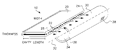
10 assembly
12 laser beam
laser diode bar
22 emitters
24 plane of emission (of each laser diode bar)
26 optical axis (of each emitter)
graded-index fiber microlens (or microlenses)
32 axis of symmetry (of each microlens)
34 graded-index core
20 36 cladding
38 antireflexion coating
mount
42 groove
laser diode array
52 array of microl~enses
DESCRIPTION
30 FIG. 1 shows a multiple emitters laser diode
assembly (10) usef~. for producing a laser beam (12)
according to a possible embodiment of the present
invention. The asse~nibly ( 10 ) comprises a single laser
diode bar (20) provided with a plurality of emitters
(22) aligned faith re~~pect to each other in a same plane
of emission (24). They laser diode bar (20) is preferably
made of GaAl~~ls but. any other suitable semiconductor
7
2162 ~2
material may lbe used, most likely the materials allowing
operation from the upper end of the visible spectrum
( about 400 nm ) to tile mid infrared ( about 5000 nm ) . A
typical wavelength is about 810 nm.
As aforesaid, in a laser diode assembly using
multiple emitters (22), the small dimension of the
emitters (22) causes a very large divergence of the beam
emitted therefrom. Typically, the divergence angle is
about 10° in the plane parallel to the diode junction
(slow axis) a:nd about 40° in the plane perpendicular to
the diode junction (fast axis). The fast axis is thus
generally collimated in priority in order to obtain an
optimum optical tran:mission of the beam emitted by all
the emitters (22). In order to collimate all the
emitters (22) at they same time, the microlens (30) is
positioned with great precision in front of the laser
diode bar (20) with its axis of symmetry (32)
(longitudinal axis) substantially intersecting the
optical axis (26) of each emitter.
The pre;~ent invention may also be used for
collimating the =slow axis by using a microlens
perpendicular to the plane of_ emission. It may further
be used to modify or control the divergence, other than
collimation, of a l~a:;er diode bar or array.
As an example, a typical laser diode bar has around
16 emitters with an even spacing between adjacent
emitters of about 550 Vim. The emitters have a width of
about 100 Vim, a th:ic;kness of about 1 um and a cavity
length (depth.) of about 500 ~,m. Of course, other
dimensions are suitable and depend on the specific
needs, like the mode of operation (pulse or continuous),
the peak power, the duty factor, etc. Some
specification; may r>e required to obtain an optimum
performance, such a~a the tolerance of the cavity length
of the laser diode bar (20) which has to be typically ~
5 ~,m. It is important to select a suitable mechanical
tolerance in t:he de;~i.gn of a laser diode bar or array,
8
otherwise a scavere degradation of the performance may be
encountered in some situations.
According to the present invention, it has been
found that the use of a fiber microlens (30) with a
graded-index core (34) (GRIN) transversely set in front
of a laser diode b<~r (20) allows a high collimation
efficiency oi.-' the i=ast axis at high NA with a low
spherical abe~rratiori on the transmitted beam (12). A
mounting means is used for positioning the microlens
(30) with respect to the laser diode bar (20).
The microlens ( :f0 ) is def fined as an elongated f ibex
since its length i;s more important than its diameter.
The GRIN microlens (?.0) is preferably a nonfull aperture
Luneberg-type lens with a homogenous cladding (36)
obtained by a suitable process. However, the present
invention is not limited to nonfull aperture Luneberg-
type lenses and could be, for instance, a full aperture
Luneberg-type lens with or without the homogenous
cladding or a nonfull aperture GRIN with a profile
different from the Luneberg-type and with or without a
homogenous cladding. The GRIN microlens (30) may also
have a non-circular ~~ross section.
The GRIN micr~o~Lens ( 30 ) with a nonfull aperture
Luneberg-type profil~a shows high collimation efficiency
at high numerical ~~perture (NA) with low spherical
aberration on the transmitted beam. Also, since the
cross section of 1=his microlens is circular, the
performance ojF the rnicrolens is invariant over rotation,
thus allowing an easier alignment.
In orde~_° to obtain the best performance, the
mechanical dejFormations of the laser diode bar ( 20 ) must
be minimized. According to a preferred embodiment of the
present invention, this is achieved by using a mount
( 40 ) issued from a '''bars in grooves" packaging technique
as shown in FIGS . °_i and 6 . The advantage of the mount
(40) is that it is possible to precisely align the
emitters of a laser diode bar or bars (20) with respect
9
2165262
to their plane of emission (24) (parallelism and period)
and, in the c:ase of a laser diode array, align the bar
facets in the same ~>lane within the depth field of the
array of mic~~olense:~. The mechanical precision of the
alignment is preferably between 1 ~m and 10 Vim. Of
course, any other suitable mount which gives an
equivalent precision may be used.
The mount (40) acts as a spacer/holder and is
preferably made of ceramic, like BeO, but other
materials are suitable. It may be machined with a groove
(42) equal to the diameter of the microlens (30). It is
further slightly longer than the corresponding laser
diode bar (20) and the groove (42) is cut entirely
through the ceramic material. This may be machined by
conventional means, such as a diamond saw or a laser
machining. In such m~~unt ( 40 ) , the microlens ( 30 ) is set
in the groove (42) and is fixed, for instance, by means
of an adhesive at :ita ends or by a mechanical pressure
therein. The mount (40) will allow a greater precision
in alignment.
It has )r~een said that all emitters (22) of a laser
diode bar (20) are cm the same plane of emission (24).
This plane of emis:~ion (24) is defined by the facet
thickness and.the width of the laser diode bar (20). All
the emitters (22) are on the same axis which is
perpendicular to th.e cavity length. Also the position of
the microlen:~ (30) with respect to the laser diode bar
(20) should be controlled with great accuracy. The
optical axis of al.l the emitters (22) should pass
through the axis of :symmetry of the GRIN microlens (30).
The separation between the GRIN microlens (30) and the
laser diode bar (20), more particularly the distance
between the emitting surface of the laser diode bar (20)
and the outside diameter of the GRIN microlens (30)
closest to the la:~E:r diode bar ( 20 ) , has to be kept
constant and equal t.o the back focal length of the GRIN
microlens (30) in order to collimate it.
216262
Preferably, th~~ microlens (30) may further comprise
an antireflexion coating (38) in order to optimize its
transmission.
As aforesaid, t:he present invention may be used
with a laser diode array (50). The laser diode array
(50) comprises a plurality of substantially parallel
rows of emiti:ers with a substantially regular period
(spacing) between them. Each row comprises multiple
emitters ( 22 ) aligned with respect to each other in a
same plane of emission (24). It should be noted at this
point that the rows of emitters may be laser diode bars
(20), as shown in the drawings, or rows of a matrix of
emitters. The rows may be vertical, horizontal, or in
any other specified direction.
An array (52) of graded-index elongated fiber
microlenses (:30), substantially parallel to each other,
is facing the rows: of emitters. Each microlens (30)
corresponds to one of the laser diode bar (20) for
collimating the corresponding beam generated thereby.
The period betwee~r,~ adjacent microlenses (30) is
substantially corres~~onding to the one of the rows.
Each microlens ( 30 ) is transversely set in front of
the corresporn~ing row and has an axis of symmetry (32)
substantially inter~;ecting the optical axis of each
emitter thereof. Mounting means are provided for
positioning each microlens with respect to the
corresponding row.
The emitters ( 22 ) of a row should be in the same
plane of emis:~ion (2~~). All rows should also be aligned
with respect to each other in order that the
corresponding emitters (22) from adjacent rows be
aligned with each other. All those mechanical alignments
should be realized ~w:lth the highest possible precision,
preferably in the order of a few microns. FIG. 4A
schematically shows. a laser diode array (50) with no
error in the alignmmnt of laser diode bars (20). FIGS.
4B to 4D show diffe:rE~nt typical errors in a laser diode
11
2~ 6262
array (50) tlhat m~~~~ affect the performances of the
collimation. =Cn part:Lcular, FIG. 4B shows a laser diode
array (50) with errors in the parallelism of the laser
diode bars (20). FIG" 4C shows a laser diode array (50)
with errors in the spacing of the laser diode bars (20).
FIG. 4D shows a la:ae~r diode array ( 50 ) with errors in
the vertical alignment of the laser diode bars (20).
EXAMPLE
An expeniment;~l_ comparison of the collimating
performances c>f different microlens has been realized in
order to evaluate the GRIN fiber microlenses with a
multiple emiiaers Laser diode assembly. The GRIN
microlens was a nonf~all aperture Luneberg-type lens of
400 ~m with a back focal length of 70 ~m and a NA of
0,50. It was compared to an ordinary fiber lens (fused
silica cylindrical fiber) with a diameter of 400 um, 100
~m of back focal length and a NA of 0,50. The third lens
used was an a~spheric:al fiber lens with AR ( BLUE SKYT'''
Hyperbolic fiber microlens) of 250 ~m x 300 Vim, a back
focal length of 110 ~m and a NA of 0,56. No
antiref lexion coating was present on the two other f fiber
microlenses and all of them were compared using the same
laser diode bar. The results were as follows:
Microlens Divergence (deg) Optical Transmission
aspherical 1,44 0,745
ordinary 1,08 0,773
GRIN 0,90 0,837
The best trans>mission and collimation were thus
obtained with the GRIN fiber microlens.
12
216 ~2 62
In another ex;pEariment, the fast axis of a laser
diode array of 64 laser diode bars was collimated with
an array of GRIrt fiber microlenses as described
hereinabove. The results is an overall divergence beam
in the fast axis of 2 degrees with a high efficiency.
Although pref~arred embodiments of the invention
have been des~~ribed .in detail herein and illustrated in
the accompanying drawings, it is to be understood that
the invention is not limited to these precise
embodiments and that various changes and modifications
may be effectE~d therein without departing from the scope
or spirit of the invention.
13