Note: Descriptions are shown in the official language in which they were submitted.
~166228
A POWER INTEGRATED CIRCUIT
BACK~ROUND OF THE INVENTION
Field of the Invention
The present invention relates to the field of semi-
conductor components, hereinafter referred to as power
components, capable of withstanding high voltages and/or
transmitting high powers. These components are vertically
disposed over the whole thickness of a semiconductive layer
from a low doped substrate so that they have high breakdown
voltages.
Discussion of the Related Art
Conventionally, such power components are thyristors,
triacs, bipolar transistors, power MOS transistors,
insulated-gate bipolar transistors (IGBTs), etc.
Components designed to control high electrical power
dissipate thermal energy. Thus, the bottom surface of these
components is metallized and mounted on a heat sink. As a
consequence, if it was desired to form several power compo-
nents on the same chip, this has only been possible when
these various components have one common terminal.
SUMMARY OF THE INVENTION
An object of the present invention is to fabricate
power integrated circuits, i.e. to group on the same sub-
strate vertical components having at least one layer
constituted by a low doped portion of this substrate, the
bottom surface of the substrate being metallized to be
welded or connected in another suitable way to a heat sink.
To achieve this and other objects, the present inven-
tion provides for monolithically assembling vertical power
semiconductor components throughout the thickness of a low
doped semiconductive wafer of a first conductivity type.
The bottom surface of the wafer is uniformly coated with a
2166228
metallization. At least some of these components, so-called
"autonomous" components, are formed in insulated sections
of the substrate. These "insulated sections" are laterally
insulated by a diffused wall of the second conductivity
type and their bottom is insulated through a dielectric
layer interposed between the bottom surface of the
substrate and the metallization of the bottom surface.
When the semiconductive region of the bottom surface of
an autonomous component is of the first conductivity type,
an overdoped region of the first conductivity type is
provided on the bottom surface and an overdoped region of
the first conductivity type, from which a contact is taken,
is provided on the upper surface above at least a portion
of the overdoped region of the bottom surface.
When the semiconductive region of the bottom surface of
an autonomous component is of the second conductivity type,
this region laterally extends up to an insulation wall, a
contact being taken again from the upper surface of the
insulation wall, the dielectric layer extending beneath the
lower foundations of the insulation wall.
In at least one insulated section, logic components can
be formed.
The present invention also applies to the fabrication
of a monolithic diode bridge including, in a substrate of a
first conductivity type, two first vertical diodes whose
common cathode corresponds to a bottom surface metalli-
zation, and, in an insulated section of the substrate (the
insulated section being separated from the rest of the
substrate by an insulation wall of the second conductivity
type), two second vertical diodes whose common anodes
correspond to a layer of the second conductivity type
formed on the bottom surface whose contact is taken from
the upper surface through the insulation wall, the bottom
surface of these two diodes being coated with an insulating
2166228
layer interposed between the semiconductive wafer and the
bottom surface metallization.
The invention also applies to a component forming a
single-phase rectifying bridge that includes first and
second pairs of head-to-tail connected diodes disposed
between a.c. supply terminals, the junctions between the
diodes of each pair of diodes constituting a d.c. supply
terminal, and two head-to-tail Shockley diodes in anti-
parallel with the diodes of the first pair of diodes. The
Shockley diodes and the first pair of diodes are vertically
disposed in a semiconductor substrate whose upper surface
includes two first metallizations forming a.c. supply
terminals, and whose bottom surface includes a third metal-
lization forming a d.c. supply terminal corresponding to
the junction of the first two diodes. The second pair of
diodes is disposed in an insulated section between a fourth
metallization forming a d.c. supply terminal and each
metallization forming an a.c. supply terminal.
According to an advantage of the invention, a plurality
of vertical components can be formed on a same semiconduc-
tive substrate, first vertical components having a common
electrode constituted by the bottom surface metallization,
and second components being autonomous, i.e., their
electrodes can be separately connected to various terminals
of other components or to external terminals, none of these
electrodes being constituted by the metallization of the
bottom surface.
In addition, since the bottom surfaces of the autono-
mous components are protected by a thin insulating layer,
such as a silicon oxide layer, in turn coated with the
bottom surface metallization, good heat dissipation is
obtained, even for the components whose bottom surface
includes this thin layer that is electrically insulating
but remains thermally conductive.
2166228
Although only some specific components that can be
assembled to form a power integrated circuit, as well as
possible associated logic circuits and some applications
thereof, are described below, the invention is not limited
to these particular cases. Those skilled in the art will
note an analogy between the autonomous components according
to the present invention and individual components of a
bipolar integrated circuit. Indeed, in bipolar integrated
circuits, most of the components of an integrated circuit
are formed in an epitaxial layer, the individual components
being mutually insulated by deep diffusions going through
the epitaxial layer and their bottom being insulated by
buried layers of either conductivity type. According to the
present invention, the whole thickness of the substrate
corresponds to the epitaxial layer and the bottom junction
insulation (buried layer) is replaced with the insulating
layer which is interposed between the bottom surface of the
substrate and the bottom surface metallization. Those
skilled in the art can use this analogy to find further
variants and applications of the present invention.
The foregoing and other objects, features, aspects and
advantages of the invention will become apparent from the
following detailed description of the present invention
when taken in conjunction with the accompanying drawings.
BRIEF DESCRIPTION OF DRAWINGS
Figs. lA and lB are a cross-sectional view and a
schematic view, respectively, of various types of diodes
that can be assembled according to the present invention;
Figs. 2A and 2B are a cross-sectional view and a
schematic view, respectively, of various types of
thyristors that can be assembled according to the present
invention;
Figs. 3A and 3B are a cross-sectional view and a
schematic view, respectively, of various types of NPN
- 2166228
transistors that can be assembled according to the present
invention;
Figs. 4A and 4B are a cross-sectional view and a
schematic view, respectively, of various types of PNP
transistors than can be assembled according to the present
invention;
Fig. 5 represents an exemplary cross-sectional view of
an autonomous IGBT transistor that can be monolithically
integrated according to the present invention;
Figs. 6, 7, 8 and 9 are generalized representations of
the various types of components that can be monolithically
assembled according to the present invention;
Fig. lOA represents a diode bridge; Figs. lOB and lOC
are a cross-sectional view and a schematic top view,
respectively, of an embodiment according to the present
invention of such a diode bridge; and
Figs. llA, llB, llC, 12A, 12B, 13A, 13B, 14A, 14B, and
14C illustrate an application of the present invention to a
rectifying bridge protected against overvoltages and over-
currents.
AS is conventional in integrated circuit represen-
tation, it will be noted that the various drawings are not
drawn to scale, and in particular, in the cross-sectional
views, the relative thicknesses of the various layers are
arbitrarily drawn. Also, in the cross-sectional views, the
various diffused regions are symbolically drawn with
squared corners. In addition, in each case, those skilled
in the art can adapt the relative surfaces of the various
regions to comply with the required power performance of
the component.
It will be clear for those skilled in the art that the
present invention describes only basic structures of compo-
nents and that, in practice, each of these components can
be improved and modified to meet specific required
functions. For example, thyristors only, and not triacs,
~ 2166~28
are represented and, in most figures, the anode or cathode
shorts of these thyristors are not shown.
DETAILED DESCRIPTION
EXEMPLARY COMPONENTS THAT CAN BE ASSEMBLED ACCORDING TO THE
INVENTION
Fig. lA represents various types of diodes 10 to 14
that can be assembled on a same N-type semiconductive
wafer. Fig. lB symbolically represents each diode of Fig.
10 lA. The structure is formed from a low doped N-type
substrate 1. P-type diffusions 2 can be formed from the
upper surface, as well as highly doped N-type diffusions 3.
From the bottom surface, highly doped N-type diffusions 4
and highly doped P-type diffusions 5 are formed. In
addition, P-type insulation walls 6 are formed from an
upper surface diffusion and from a facing bottom surface
diffusion. The whole bottom surface is coated with a
metallization M. At some places, an insulating layer 7 is
interposed between the bottom surface of the component and
metallization M. The insulating layer 7 and metallization M
can be made of any suitable material or composite material
conventionally used for the manufacturing of semiconductive
components.
Hereinafter, "insulated section" is to be construed as
designating a portion of a silicon wafer laterally
insulated by a wall of the second conductivity type and
having a bottom insulated by an insulating layer 7.
Diodes 10 and 11 are conventional diodes provided in a
power component. Diode 10 vertically includes, from top to
bottom, a P-type region, a substrate portion and a N-type
region; the upper surface metallization corresponds to its
anode lOA and its bottom surface metallization M
corresponds to its cathode lOK. Diode 11 vertically
includes, from top to bottom, a highly doped N-type region,
a portion of the substrate and a highly doped P-type
~1~622~
region; its cathode llK corresponds to an upper surface
metallization and its anode corresponds to metallization M.
This conventional implementation of diodes lO and 11
causes those diodes to have one common terminal. Further-
more, for example, it is impossible to make from suchdiodes a monolithic diode bridge, in which the diagonally
opposed diodes have no common terminal.
Diodes 12 and 13 are "autonomous" diodes, formed in
insulated sections according to the present invention,
which have the advantage of vertically operating and of
having anode and cathode electrodes which are not neces-
sarily common to the electrodes of other components of the
circuit.
Diode 12 vertically includes, from top to bottom, a P-
type region which corresponds to its anode, a substrate
portion and a highly doped N-type region which corresponds
to its cathode. Thus, diode 12 is a vertical diode. In
addition an N-type region is formed on the upper surface,
contacting a cathode metallization 12K.
Diode 13 vertically includes, from top to bottom, an N-
type region corresponding to its cathode 13K, a substrate
portion and a P-type region diffused from its bottom
surface. An anode metallization 13A is formed on the upper
surface of the insulation wall, which delineates the
insulated section in which diode 13 is formed.
The right portion of Fig. 1 also represents a lateral
diode 14 also formed in an insulated section. Diode 14
includes an N-type region contacting a cathode metalli-
zation 14K, formed in a P-type well which is diffused in
substrate 1 and contacts an anode metallization 14A. Diode
14 is not a power component since it operates laterally and
could form an element of a logic circuit associated on a
same chip with one or more power components. An aspect of
the present invention is also to dispose logic circuits in
insulated sections because it was impossible as a practical
216G22g
matter, to integrate such logic elements to power
structures when the power structures included four-layer
components because of the unavoidable occurrence of
spurious vertical thyristors.
It should be noted that the integration of four-layer
components (thyristor-type) always raises operation
problems for the components integrated in the same chip.
Indeed, through lateral coupling, an integrated diode or
thyristor forms with other layers of the structure a
spurious thyristor whereby the structure may be short-
circuited in response to triggering of this spurious
thyristor and will therefore not fulfill the required
function. In the present case, the lateral and bottom
insulations prevent these spurious thyristors, which allows
the safe integration of thyristor components with other
logic or power components.
Figs. 2A and 2B illustrate various thyristor structures
that can be used according to the present invention.
The left-hand portion of Fig. 2A illustrates conven-
tional thyristors 20 and 21 whose respective anode andcathode are connected to a bottom surface metallization.
Thyristor 20 includes a vertical N-type region corre-
sponding to its cathode 20K, a P-type region from which a
gate contact 20G is taken, a substrate portion 1 and a P-
type anode region contacting metallization M whichcorresponds to anode 20A of the thyristor. Also, Figs. 2A
and 2B show a lateral insulation wall of this thyristor;
however, this insulation wall has not in this specific case
an insulating function but is conventionally used to form a
well-type thyristor capable of withstanding high voltages.
Thyristor 21 is a complex component such as described
in US patent 5,365,086 assigned to the applicant and is
represented to clearly demonstrate that the present inven-
tion makes it possible to assemble in a single power
circuit practically any known elementary component.
- Z16fi228
The right-hand portion of Fig. 2A represents
"autonomous" thyristors 22 and 23 formed in insulated
sections.
Thyristor 22 is a vertical power thyristor which
includes, from top to bottom, an N-type region, from which
are taken the cathode metallization 22K, a P-type region,
an N-type substrate portion and a P-type region formed from
the bottom surface and contacting an insulation wall 6 on
the upper surface of which an anode metallization 22A is
taken.
Thyristor 23 is a lateral thyristor which can be part
of a logic circuit. Thyristor 23 includes an N-type cathode
region contacting a metallization 23K formed in a P-type
region from which the gate contact 23G is taken, this P-
type region being formed in the substrate. In the samesubstrate is formed a P-type region contacting the anode
metallization 23A. As mentioned above, an advantage of
disposing such a lateral thyristor in an insulated section
of the wafer is that the layers constituting this thyristor
therefore do not constitute spurious elements with other
elements of the structure.
Fig. 3A represents three exemplary NPN transistors 30,
31, 32 fabricated according to the present invention.
Transistor 30 is a conventional vertical transistor
which includes an N-type region contacting the emitter
metallization 30E, a P-type region contacting the base
metallization 30B. This P-type region is formed in a
substrate portion and a highly doped N-type region is
formed in the bottom surface and contacts the bottom
surface M which corresponds to the collector.
Transistors 30 and 31 are formed in insulated sections
of the substrate.
Transistor 31 is similar to transistor 30, but
includes, on its upper surface, an additional highly doped
N-type region facing a portion of the N-type region of the
- 2166228
lower surface; this additional N-type region is connected
to a collector metallization 31C.
Transistor 32 is a lateral transistor and includes, in
a P well, N-type regions contacting emitter metallization
32E and collector metallization 32C, respectively, with
region P contacting a base metallization 32B. Transistor 32
can constitute an element of a logic circuit associated
with one or more power components.
Similarly, Fig. 4A represents three types of PNP
transistors 40, 41, 42 which can be fabricated according to
the present invention.
The PNP transistor 40 is a conventional power transis-
tor whose bottom surface corresponds to metallization M and
which includes, on the upper surface of the substrate, a P-
type region contacting an emitter metallization 40E and an
N-type region contacting a base metallization 40B. A P-type
region contacting the substrate is formed on the bottom
surface. Preferably, this P-type region contacts the
insulation walls.
Transistor 41 is formed in an insulated section. Its
structure is generally the same as that of transistor 40,
but the collector contact 41C is taken from the upper
surface of the lateral insulation wall.
Transistor 42, also formed in an insulated section, is
a PNP lateral transistor complementary to the lateral
transistor NPN 32, described above.
Thus, the components illustrated in Figs. 1-4 represent
elements of a library of cells of power or logic components
which can be assembled on a same layer according to a
desired design.
Depending upon the desired requirements, there is
formed power components with a common electrode, or autono-
mous components formed in one or more insulated sections
with electrodes distinct from those of the other components
of the same chip.
216622~
Of course, the components of Figs. 1-4 are only
exemplary elementary components that can be used. Any
conventional power component can effectively be used in
monolithic integrated power structures according to the
invention. For example, those skilled in the art can easily
transform thyristor structures, illustrated in Fig. 2, into
triac structures, and can also use both anode-gate
thyristors and cathode-gate thyristors.
For the sake of simplification, all the alternatives
have not been represented and described. In particular,
referring to Fig. 2A, it can be seen that the middle low
doped N layer, is not fully used; in fact, an additional
so-called "anode gate" electrode can be connected thereto.
The manufacturing process is not more complex since this
layer is anyhow apparent on the upper surface. Then, each
thyristor can be controlled through its cathode gate (not
shown) or this anode gate (not shown).
The above description is purposely simplified. In some
cases, it is possible and desirable to dispose various
components in a same well (with or without insulation of
the bottom surface). By way of example, diode 11 can be
disposed in the same well as thyristor 21.
With the same rules, passive elements, such as
resistors and capacitors can also be added to an integrated
circuit according to the present invention.
Moreover, the bottom surface metallization of the
component, mainly designed to provide good thermal connec-
tion with a heat sink, is not necessarily connected to an
external terminal and can merely constitute an internal
junction of elementary components of the power integrated
circuit. The metallization can also be electrically
insulated from a heat sink structure.
By way of example only, to clearly show the wide range
of applications of the present invention, Fig. 5 represents
an IGBT transistor fabricated according to the present
`- ~166228
invention in the form of an autonomous component in an
insulated section of a semiconductive wafer.
Fig. 5 shows again the conventional structure of an
IGBT transistor, including, on the upper surface of a
substrate 1, a P-type region in which are formed N-type
regions extending near the periphery of the P-type region
so as to define areas where a channel may be formed, the
upper surface of these areas being insulated and covered
with a gate metallization G. A collector metallization C
contacts N-type regions and a central overdoped portion of
the P-type region. A P-type region 5 is also formed from
the bottom surface of the substrate. In a conventional
structure, P-type region 5 contacts the metallization M of
the bottom surface substrate which constitutes its emitter.
Here, to render the component autonomous, an insulating
layer 7 is formed between the P-type region and metalli-
zation M, and the component is surrounded by a P-type
insulation wall 6. Emitter contacts E are taken from the
upper surface of this wall.
Thus, it should be noted that, with the present inven-
tion, components of the MOS-type and of the bipolar-type
can be associated in a same power integrated circuit.
GENERALIZED DISCLOSURE OF THE INVENTION
Figs. 6-9 illustrate, in a generalized conceptual way,
the various types of components that can be monolithically
fabricated and assembled according to the present
invention.
As represented in Fig. 6, conventional vertical compo-
nents can be directly formed in an N--type substrate 1
whose bottom surface is coated with a metallization which
corresponds to a common electrode of these various vertical
components.
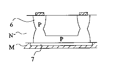
As represented in Fig. 7, a first category of autono-
mous components can be formed in an insulated section of
622~
the substrate, these components having on their bottomsurface an active layer 4 of the same conductivity type as
the substrate, but more highly doped. This layer is sepa-
rated from the bottom surface metallization M by an
insulating layer 7, and the contact with this layer is
established through an additional highly doped region 3
formed on the upper surface of the substrate, which is of
the same conductivity type as the substrate and faces at
least a portion of layer 4. Of course, in this case, there
will exist a resistance because of the substrate thickness
between regions 3 and 4; so, this type of structure is
preferably used for components liable to withstand high
voltages but not designed to withstand high current
densities.
As represented in Fig. 8A, a second category of autono-
mous components can be formed in an insulated section of
the substrate. These components have on the bottom surface
an active layer of the conductivity type opposite to the
conductivity type of the substrate. In this case, contact
is taken through the insulation walls 6. Since these
insulation walls can be relatively highly doped, such
components can be used as high power components. In this
case, the insulating layer 7 should lie beneath the bottom
surface of the component and extend up to the external
limits of the insulation walls.
Fig. 8B represents an alternative embodiment wherein
the P region of the lower surface is a relatively thick
region substantially occupying one half of the thickness of
the substrate and joining an insulation wall 6 formed from
the upper surface.
As represented in Fig. 9, a third category of autono-
mous components can be formed in an insulated section of
the substrate. These components are designed to constitute
logic circuits elements formed in a well 10 having a
conductivity type opposite to that of the substrate.
- 2166228
14
DIODE BRIDGE
An exemplary application of the monolithic assembly
mode of power components according to the present invention
is described hereinafter in relation to a diode bridge. A
diode bridge, represented in Fig. lOA, includes four diodes
Dl-D4. The common anode of diodes D2 and D4 constitutes the
negative bridge terminal T-; the common cathode of diodes
D1 and D3 constitutes the positive bridge terminal T+; the
junction of diodes D1-D2 and D3-D4 constitutes the a.c.
supply terminals T1 and T2, respectively, of the bridge.
Fig. 10B is a cross-sectional view of an embodiment
according to the present invention of the diode bridge of
Fig. lOA. Fig. lOC is a top view of the diode bridge. Fig.
lOB is a cross-sectional view along lines B-B of Fig. lOC.
As illustrated in Figs. lOB and lOC, cathode-connected
diodes D1 and D3 are conventional vertical diodes and
include, on the upper surface of a low doped N-type
substrate 1, a P-type region P1, and include, on the bottom
surface, an N+-type region N2 contacting a lower metalliza-
tion M which is metallization T+ of Fig. lOA. Diodes D2 and
D4 are formed in insulated sections of substrate separated
from the rest of the substrate by a P-type wall P3 obtained
from deep diffusions achieved from the upper and bottom
surfaces using conventional techniques. The bottom surface
of these insulated regions and the bottom surface of wall
P3 are protected by a dielectric material layer 7, such as
silicon oxide. Each diode D2 and D4 includes, on its upper
surface, an N+-type cathode region N4 formed in substrate
N. These regions N4 are distinct for each diode D2 and D4.
On the bottom surface, a P-type region P5 constitutes the
common anode of diodes D2 and D4. The anode contact is
taken from a metallization T-. A metallization T1 connects
region P1 with region N4 whereas a metallization T2 (refer
~166228
to Fig. lOC) connects the corresponding region of diode D3
to the corresponding region of diode D4.
In the top view, areas where metallizations T1 and T2
are contacting the semiconductive underlying areas are
represented by crosses, the remaining portions of these
metallizations being formed on an oxide layer.
PROTECTED RECTIFYING BRIDGE
Fig. llA illustrates a rectifying bridge including four
diodes Dl-D4 connected as in Fig. lOA.
To protect the diodes of the bridge and especially the
components that can be connected to terminals T+ and T-, a
bidirectional protection component S is usually used, such
as a double Shockley diode disposed between terminals Tl
and T2. This protection component allows, for example,
protection against lightning that may strike a telephone
line, or overvoltages caused by the contact between a
telephone line and a mains line.
The circuit, represented in Fig. llA, using a double
Shockley diode as a protection element operates correctly,
but needs the association of several discrete elements: a
double Shockley diode, and a rectifying bridge. The bridge
is also frequently fabricated in the form of two silicon
components, each integrating a branch of the bridge, and
which are mounted in the same casing.
It will be shown that the present invention allows the
fabrication of such a bridge protected against overvoltages
or overcurrents in the form of a monolithic component.
The present invention is based on an analysis of the
circuit of Fig. llA. The applicant has modified this
circuit in order to fabricate it in a monolithic form. In
particular, the applicant proposes alternative embodiments
of the circuit of Fig. llA such as depicted in Figs. llB
and llC.
-~ 21~6228
16
In the circuit of Fig. llB, diode S is replaced by two
head-to-tail unidirectional Shockley diodes, Sl and S3,
connected between terminals T1 and T2, and whose common
anode is connected to the common cathode of diodes D1 and
D3.
In the circuit of Fig. llC, diode S is replaced by two
head-to-tail unidirectional Shockley diodes, S2 and S4,
connected between terminals T1 and T2, and whose common
cathode is connected to the common anode of diodes D2 and
D4.
In Figs. llB and llC, diodes Dl-Sl, D3-S3, and D2-S2,
D4-S4, respectively, have been disposed closer together be-
cause, as will be seen hereinafter, the proposed embodiment
in the form of a monolithic component more particularly
combines these diodes that have common terminals.
The component illustrated in Figs. 12A and 12B, that
implements the circuit of Fig. llB, is fabricated using a
low doped N-type silicon wafer 1. As shown in Figs. 12A and
12B, the Shockley diodes S1 and S3, as well as diodes D1
and D3 connected in anti-parallel, are disposed vertically
in the left-hand portion of the component, and diodes D2
and D4 are disposed in an insulated section in the right-
hand portion of the component.
The left-hand portion of the component includes two P-
type wells 10 and 11 formed from the upper surface ofsubstrate 1. In substantially one half of the surface of
each well 10 and 11 is formed an N-type region, 12 and 13,
respectively, which constitutes the cathode of a Shockley
diode S1, S3. Regions 12 and 13 are conventionally
discontinuous so that portions of the material of wells 10,
11 extend upwardly through apertures provided in regions
12, 13 to form so-called emitter shorts. Substantially
beneath each region 12 and 13, are formed from the bottom
surface of the substrate P-type regions; in Fig. 12A, only
region 14 disposed beneath region 12 is visible. These P-
~166228
type regions constitute the anodes of the Shockley diodes.Beneath the portion of wells 10 and 11 that does not
include the N-type regions 12 and 13, is formed from the
bottom surface of the substrate an N+-type region, of which
only region 16 corresponding to the cathode of diode Dl is
visible. Preferably, beneath region 12 (and symmetrically
beneath region 13), at the interface between region 10 and
substrate 1, an N-type region 17, that is more highly doped
than the substrate, sets the breakover voltage of the
Shockley diodes.
Diodes D2 and D4 are formed in the right-hand portion
of Figs. 12A and 12B. These diodes are disposed in insu-
lated sections. In the embodiment of Fig. 12, the insulated
sections are formed from a deep P-diffusion 18 extending
from the upper surface and joining a deep P-diffusion 20
that is formed from the bottom surface. These P-type diffu-
sions 18 and 20 delineate in the substrate two N-type wells
22 and 23 inside which are formed overdoped N+-type areas,
24 and 25, respectively. The junction between the N-type
well 22 and the P-type diffusions 18, 20 corresponds to
diode D2, and the junction between the N-type well 23 and
the P-type diffusions 18, 20 corresponds to diode D4.
The bottom surface of the P-type deep diffusion 20 is
coated with an insulation layer, usually a silicon oxide
layer, 26. Similarly, the upper surface of the component is
coated with a silicon oxide layer, 27, etched at the places
where it is desired to establish contacts between areas of
the component and metallizations.
The bottom surface of the component is uniformly coated
with a metallization that corresponds to terminal T+ of the
circuit of Fig. llB. Referring to the top view, the metal-
lization outline is drawn in dotted lines in Fig. 12B. A
- first metallization, corresponding to the a.c. supply
terminal T1, contacts the upper surface of the N-type
region 12, of well 10 and of the N+-type region 24. A
2166228
18
second metallization T2, corresponding to the second a.c.
supply terminal T2, is symmetrically laid upon layer 13,
well 11, and the upper surface of the N+-type region 25.
The upper surface of the P-type deep diffused region 18 is
coated with a metallization corresponding to terminal T-.
To fabricate a monolithic component corresponding to
the circuit of Fig. llC, the drawing of Figs. 12A and 12B
could be used by inverting all the conductivity types of
the various layers. In practice, however, for technological
reasons, it is often preferable to fabricate a monolithic
component from an N-type semiconductor substrate.
Figs. 13A and 13B are a cross-sectional view and a top
view, respectively, of an embodiment of a monolithic compo-
nent according to the invention corresponding to the
circuit of Fig. llC. The component is formed from an N-type
substrate, labeled 1 as previously. Diodes S2, D2, S4, S4
are disposed in the right-hand portion of the figure, and
diodes Dl, D3 are disposed in the left-hand portion.
The whole component is surrounded with a P-type wall 30
formed by the junction of an ascending diffusion and a
descending diffusion that are realized from the bottom and
upper surfaces. Simultaneously, a central wall 31,
partitioning the wafer into two portions, is formed.
Additionally, a wall 32 (refer to Fig. 13B) separates the
regions where diodes D2-S2 and D4-S4 are formed.
The Shockley diode S2, visible in the cross-sectional
view of Fig. 13A, includes, from the upper surface of the
substrate, a P-type anode region 40, the N-type substrate
1, a P-type region 42 formed from the bottom surface and in
which is formed an N-type region 44 provided, as the region
12 of Fig. 12, with emitter shorts. An N+-type region 46 is
formed at the interface of the P-type region 42 and of the
N-type substrate to set the triggering threshold of the
Shockley diode.
~1 66228
19
Diode D2 includes, from the upper surface to the bottom
surface, an N+-type region 50 that is adjacent to region
40, and that constitutes the cathode of diode D2. It also
includes the N-type substrate, and an extension of the P-
type region 42 that corresponds to the anode.
Diodes S4 and D4 are identical to diodes S2 and D2;
they are represented as a top view in Fig. 13B that also
shows regions 41 and 51 which correspond to regions 40 and
50, respectively.
Diodes Dl and D3 are formed in the left-hand portion of
Fig. 13B, that is delineated by the insulation wall 30, 31.
In the upper surface of the substrate are formed P-type
regions 52 and 53 corresponding to the anodes of diodes D1
and D3, respectively, and an N+-type region 54 correspond-
ing to the common cathodes of diodes Dl and D3. The bottom
surface of the well that is delineated by the insulation
walls 30, 31 is coated with an insulation layer 55.
A metallization is formed on the bottom surface and
corresponds to terminal T- of Fig. llC. A metallization is
formed on the N+-type region 54 and corresponds to terminal
T+. A metallization corresponding to terminal Tl coats the
P-type region 52, the N+-type region 50 and the P-type
region 40. A metallization corresponding to electrode T2
coats regions 53, 51 and 41.
It will clearly appear to those skilled in the art that
the top views of Figs. 12B and 13B are illustrative only.
These top views are schematic and various shapes can be
chosen by those skilled in the art, more particularly for
the choice of the active areas of the various elements of
the component, to provide desired conduction performance.
According to an alternative aspect, the present inven-
tion provides a component, also realized in a monolithic
form, capable of constituting a rectifying bridge protected
both against overvoltages and against overcurrents.
- 2166228
Fig. 14A is a diagram of a circuit providing such func-
tion. The Shockley diodes correspond to thyristors having
their gates connected to terminal T-, which is connected
through a resistor R to the junction of the cathodes of
these thyristors and to the junction of the anodes of
diodes D2 and D4. Thus, components S2 and S4 can operate
either as Shockley diodes, as above described, in case of
an overvoltage, or as thyristors when the current in
resistor R, i.e., the current in the rectifying bridge,
exceeds a predetermined threshold.
Figs. 14B and 14C are a cross-sectional view and a top
view, respectively, of a monolithic component, developed
from the component of Figs. 13A and 13B, allowing for the
formation of the circuit of Fig. 14A. This component, on
the left of a line a-a, is identical to the component
illustrated in Figs. 13A and 13B except that the bottom
surface metallization is not connected. Same elements are
designated with same reference characters, and the left-
hand portion of Figs. 14B and 14C will not be described
again.
In the right-hand portion of the component of Fiys. 14B
and 14C, on the bottom side, layer 42 is prolonged, as is
the bottom surface metallization. On the upper side, addi-
tional P-type regions 60 and 61, not contacting the P-type
region 40, extend to the P-type wall 30. N-type regions 62
and 63 are diffused in regions 60 and 61, respectively.
A metallization connected to terminal T- contacts the
P-type regions 60 and 61 on the side of these regions oppo-
site to wall 30, the N-type diffusions 62 and 63 being
disposed between this metallization and wall 30. Thus, the
component bottom surface that previously formed terminal T-
is in this case connected to terminal T- through wall 30
and the pinched off resistors, with respective values 2R,
disposed beneath the N-type diffusions 62 and 63. An
additional metallization 64, not connected to an external
~166228
terminal, is formed on the upper surface of wall 30 and of
regions 62 and 63. Under normal operation, the parallel
resistors 2R are connected between an input terminal of the
bridge and the output terminal T- of the bridge.
Should an overvoltage occur and render, for example,
the Shockley diode S2 conductive, this overvoltage is
drained off through diode S2 and diode D4 following the
path including metallization Tl, the P-type region 40, the
N-type substrate, the P-type region 42, the N-type region
44, the bottom surface metallization, the P-type region 42,
substrate 1 and the anode region 51 of the diode D4
connected to metallization T2. This path is not shown in
the cross-sectional view of Fig. 14B drawn along line B-B
of Fig. 14C since it involves the lower portion of the top
view of Fig. 14C.
Now, assume that, during normal operation of the recti-
fying bridge Dl-D4, an overcurrent occurs while a current
flows between terminal Tl and terminal T- through diode D2,
that is, the current follows the path from metallization
Tl, region 50, substrate 1, region 42, the bottom metalli-
zation, wall 30, towards metallization T-. Between wall 30
and metallization T-, the current is split in two
fractions; one fraction passes through layer 60 beneath
region 62, the second fraction passes through layer 61
beneath region 63. Each path has a resistance equal to 2R.
Hence, the equivalent resistance is equal to R. When the
current in the resistor pinched off beneath the diffused
region 62 or 63 exceeds a predetermined value and the
voltage drop across this resistor exceeds 0.7 volt, the PN
junctions 60-62, and 61-63 become conductive. Junction 61-
63 is part of a thyristor in which the N-type region 63
constitutes the cathode, the P-type region 61 constitutes
the cathode gate region, the substrate constitutes the
base, and the P-type region 40 or 41 constitutes the anode.
Hence, this thyristor becomes conductive, and charges are
21G6 228
injected into the substrate 1, which triggers the vertical
Shockley diode S4. Then, the overcurrent is drained off
through the Shockley diode S4 and diode D2 through a path
not visible in the cross-sectional view of Fig. 14B.
The above described case corresponds to the case when
the overcurrent occurs while terminal T2 is more positive
than terminal Tl. In this case, shorting occurs while
diodes S4 and D2 are forward conducting, as indicated
above. When terminal T1 is more positive than terminal T2,
the same mechanisms trigger the Shockley diode S2 and
shorting occurs through diodes D4 and S2.
Additionally, in the case above described, resistor R
(formed by two resistors 2R connected in parallel) is
integrated. It is possible to provide a resistor R external
to the casing and having an adjustable value, which allows
for the selection of the protection current threshold.
As is apparent to those skilled in the art, various
modifications can be made to the above disclosed preferred
embodiments. For example, the junction of diodes S2, S4,
D2, D4 (Fig. llC), or the junction of diodes Sl, S3, Dl, D3
(Fig. llB) can be connected to an external terminal through
an additional diode connected in anti-parallel with an
additional Shockley diode to provide protection with
respect to a reference voltage, such as ground. Then, it is
preferable, in the case of the circuit of Fig. 12B, to
duplicate the vertical structure including the assembly Sl-
Dl or the assembly S3-D3 and, in the embodiment of Fig.
13B, to duplicate the vertical pattern including the
assembly S2-D2 or S4-D4.
These exemplary applications are illustrative only of
the numerous possibilities existing in the design of high
voltage power integrated circuit according to the invention
allowing to fabricate autonomous power components in
"insulated sections" of a substrate.
21 662~8
Having thus described at least one illustrative embodi-
ment of the invention, various alterations, modifications,
and improvements will readily occur to those skilled in the
art. Such alterations, modifications, and improvements are
intended to be within the spirit and scope of the
invention. Accordingly, the foregoing description is by way
of example only and is not intended to be limiting. The
invention is limited only as defined in the following
claims and the equivalents thereto.