Note: Descriptions are shown in the official language in which they were submitted.
6~ o
2166376
OUTPUT CONTROL CIRCUIT FOR TRANSMISSION POWER
AMPLIFYING CIRCUIT
BACKGROUND OF THE INVENTION
The present invention relates to an
transmission power amplifying circuit and, more
particularly, to an output control circuit for
amplifying the digital signals such as a digital
radio transmitter.
In a radio transmitter of a TDMA system using a
modulation system in which FM or other modulation
carrier signals have certain envelope in general,
the intermitted transmission of the power signal
having sharp rise and fall waveform edges such as a
burst signal causes a spread of the transmission
power spectrum due to the abrupt change of the
carrier wave amplitude at the rising and falling
edges. This results in undesirable influence to the
adjacent channels such as inter modulation.
Attempts have been made to mollify such sharp
rising and falling edges by controlling the signal
waveform. For example, Japanese Patent Laid-Open
No. 59-226519 proposes a circuit as illustrated in
Fig. 5 of the accompanying drawings for such
purpose. Referring to the circuit diagram, a
rectangular burst signal is applied to a burst
signal input terminal BIN in response to a burst
carrier signal. Upon receiving the burst signal, a
control waveform with a gentle change in time is
-. 216G376
~,
produced by a waveform generating circuit 14 to
control a control circuit 12.
On the other hand, the burst carrier signal
from the input terminal IN is amplified by the
preamplifier 11 and supplied to a power amplifying
circuit 13 as an input signal having an envelope
similar to that of the control waveform. The
envelope of the input signal is modified to make the
gentle rising and falling slope waveform around the
operation range of the power amplifying circuit,
thereby suppressing the spread of spectrum.
Japanese Patent Laid-Open Publication No.
5-316012 discloses another method of suppressing the
spectrum spread by using a control voltage having a
trapezoidal waveform to produce the envelope of the
transmission output signal having the trapezoidal
waveform with rising and falling edges of desired
slopes.
While a number of methods including the above
cited methods have been proposed to suppress the
spectrum spread by using gentle rising and falling
edges. However, these methods merely try to make
the rising and falling edges gentle, causing the
following problems. It is true that the gentle
rising-and falling edges suppresses the spread of
the power spectrum. More gentle rising and falling
edges necessitates a considerably longer time to
obtain a predetermined level of the transmission
- 2166371~
power signal, degrading the output response time
characteristic. It is therefore determine the slope
degree of rising and falling edges on the basis of
the relationship between the spread of the power
spectrum and the output response time characteristic
in the prior methods. As a result, it is very
difficult to set a sufficient gentleness of the
rising and falling edges to suppress the spectrum
spread within a desired level.
SUMMARY OF THE INVENTION
It is therefore an object of the present
invention to provide an output control circuit for a
transmission power amplifying circuit capable of
sufficiently suppressing the spread of the power
spectrum and improving the output response time
characteristic.
According to the present invention, a control
voltage signal for controlling the transmission
power amplifying circuit is formed by combining a
trapezoidal wave signal and a pulse wave signal.
The pulse wave signal having sharp rising and
falling edges is used as the control signal to
control the transmission power amplifying circuit in
a voltage range below a predetermined power level,
whereas a trapezoidal wave signal having gentle
rising and falling edges is used as the control
signal to control the transmission power amplifying
circuit in a range above the predetermined level,
` 2166376
thereby effectively suppressing the spread of the
power spectrum at a high power output level and
improving the output response time characteristic or
reducing the output response time.
According to an aspect of the present
invention, there is provided an output control
circuit for a transmission power amplifying circuit
designed to amplify the power of an input signal in
response to a control signal waveform comprising: a
trapezoidal wave generating circuit for generating a
trapezoidal wave signal having rising and falling
edges gentler than those of a burst signal; a pulse
generating circuit for generating a pulse signal
having a sharp rising edge in synchronization with
corresponding rising edge of the burst signal and a
sharp falling edge slightly delayed from
corresponding falling edge of the burst signal; and
an adder for producing either the trapezoidal wave
signal or the pulse signal, whichever having a
higher level, as the control signal.
According to another aspect of the present
invention, there is provided an output control
circuit for a transmission power amplifying circuit
designed to amplify the power of an input burst
signal in response to a control signal comprising:
a first circuit for producing a trapezoidal waveform
signal waveform which rises in response to the
rising of the input burst signal; a second circuit
2166376
-
for producing a pulse signal waveform which rises in
response to the rising of the input burst signal; a
third circuit for selectively outputting a higher
level output of the outputs from the first and
second circuits; a fourth circuit for detecting an
output level of the transmission power amplifying
circuit; and a fifth circuit for producing a
difference between the outputs of the third and
fourth circuits as the control signal.
Other objects and features will clarified from
the following description with reference to attached
drawings.
PREFERRED EMBODIMENTS OF THE INVENTION
Now, the present invention will be described by
referring to the accompanying drawings that
illustrate a preferred embodiment of the present
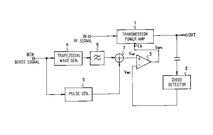
invention. Fig. 1 is a block diagram of an
embodiment to be suitably used for a transmission
power amplifying circuit having an automatic output
control function. Referring to Fig. 1, a modulated
transmission signal is supplied to a transmission
power amplifying circuit 1 through a high frequency
signal input terminal IN and amplified therein. The
amplified signal is then outputted from an output
terminal OUT. The amplification degree of the
transmission power amplifying circuit 1 is
controlled by a control voltage V~c supplied to an
output control terminal lA provided in the circuit
` 2166376
~,
1. Note that the degree of amplification or the
output level of the transmission power amplifying
circuit 1 is automatically controlled as will be
described below. More specifically, part of the
output signal outputted from the output terminal OUT
is extracted and detected by a diode detector
circuit 2 as a voltage corresponding to the output
power level. Thus detected voltage is then supplied
to one of a pair of input terminals of a comparator
3 as a detection voltage Vdet. The voltage produced
by the comparator 3 is used as a control voltage VAPC
for the transmission power amplifying circuit 1.
On the other hand, a burst signal input
terminal BIN for receiving a burst signal is
connected to a trapezoidal wave generating circuit 4
and a pulse generating circuit 5. In response to
the rising and falling edges of the burst signal,
the trapezoidal wave generating circuit 4 generates
a trapezoidal wave having gently inclined rising and
falling edges of a required voltage level. While
any circuit configuration adapted to generate the
trapezoidal wave may be used for the purpose of the
present invention, an integration circuit may be
used to generate a wave substantially equivalent to
the trapezoidal wave in this embodiment. The
trapezoidal wave generating circuit 4 can generate a
trapezoidal wave having desired gentle slope by
controlling certain parameters.
2166376
The pulse generating circuit 5 generates a
pulse signal which rises in synchronization with the
corresponding rising edge of the burst signal and
falls with slightly delayed time from the
corresponding falling edge thereof. Thus, the pulse
signal having a pulse width longer than that of the
burst signal is obtainable. The pulse generating
circuit 5 is capable of arbitrarily setting the
signal voltage level to a level lower than that of
the trapezoidal wave generated by the trapezoidal
wave generating circuit 4. A low-pass filter 6 is
connected to the output of the trapezoidal wave
generating circuit 4 to remove high frequency
components from the trapezoidal wave generated by
the circuit. The outputs of the low-pass filter 6
and the pulse generating circuit 5 are supplied to
an adder 7. The output of the adder 7 is then
supplied to the other input terminal of the
comparator 3 as the reference voltage Vref.
As seen from Fig. 2, the adder 7 comprises
operational amplifiers OPl and OP2 for receiving
respectively the trapezoidal wave signal and the
pulse signal, resistors R1 through R5 and diodes D1
and D2. The input voltages of the trapezoidal wave
signal and the pulse signal are compared by feeding
back the outputs of the operational amplifiers OP1
and OP2 and produces a higher voltage of the two
input voltages, as the output of the adder 7.
216637~
More specifically, assuming that a 3V
trapezoidal wave signal as shown in Fig. 3(a) and a
1.5V pulse signal as shown in Fig. 3(b) are supplied
to the adder 7, the higher voltage is produced so
that the pulse signal having a sharp rising edge is
produced as the output signal of the adder in the
initial stage of the rising edge until time t1, when
the rising edge exceeds the 1.5V level the output
signal of the adder is switched to the trapezoidal
wave signal. From then on, the adder 7 continues to
produce the trapezoidal wave signal as its output
until its voltage falls below the 1.5V level at time
t2, when it is switched back to the pulse signal
having the sharp falling edge.
The circuit having a configuration as
illustrated in Fig. 1 operates in a m~nn~r as
described below. As the burst signal illustrated in
Fig. 4(a) is supplied to the input terminal BIN, the
trapezoidal wave generating circuit 4 generates the
trapezoidal wave signal having a predetermined
voltage level as shown in Fig. 4(b) as its output.
The trapezoidal wave signal is then supplied to the
low-pass filter 6, where high frequency components
are removed to produce the trapezoidal wave signal
having gentler slopes.
On the other hand, as the burst signal shown in
Fig. 4(a) is supplied to the pulse generating
circuit 5, a pulse signal having a pulse width wider
2166376
~,
than that of the burst signal and a voltage level
lower than that of the trapezoidal wave signal is
produced. Supplied with the trapezoidal wave signal
and the pulse signal, the adder 7 produces a
trapezoidal wave signal having a desired profile as
- shown in Fig. 4(e). This trapezoidal wave signal is
thereafter supplied to the comparator 3 as the
reference voltage Vref. The comparator 3 produces a
difference between the reference voltage Vref and the
detection voltage Vdet obtained by the diode detector
circuit 2. This difference is supplied to a control
terminal lA of the transmission power amplifying
circuit 1 as the control voltage V~c to control the
output of the circuit 1.
Thus, the transmission power amplifying circuit
1 amplifies the high frequency signal to an extent
of amplification that corresponds to the trapezoidal
wave signal having the desired profile. Note that
the control voltage has a sharp rising edge
corresponding to that of the pulse signal in the
initial stage of rising and then shifts to gentler
rising edge corresponding to that of the trapezoidal
wave signal in the latter stage of rising as
typically illustrated in Fig. 4(e). Accordingly,
while the transmission power spectrum is spread in
the initial stage of rising, such spread of spectrum
may not be caused in any significance because of its
low output level. When the output level is
2166376
-
increased, the spectrum spread can be effectively
suppressed as the control voltage is switched to the
gentler rising edge of the trapezoidal wave signal.
The above description may also be applied to
the case of falling edge of the control voltage. In
the initial stage of falling edge of the control
voltage, the gentler inclination of the trapezoidal
wave signal is selected for the falling edge to
effectively suppress the spread of the spectrum
until the voltage level goes below a given level,
and the sharp falling inclination of the pulse
signal is selected thereafter. Consequently, the
operation of the transmission power amplifying
circuit 1 is dominated by the sharp rising and
falling edges of the pulse signal in a voltage range
below the predetermined voltage level, and by the
gentle rising and falling edges of the trapezoidal
wave signal in a voltage range higher than that the
predetermined voltage level, the response time
characteristic of the transmission power signal is
improved and the spectrum spread is effectively
suppressed.
In practice, priority may be given to either
the suppression of the spread of transmission power
spectrum or the improvement of output power response
time characteristic, or to the both, taking their
balance into account by appropriately controlling
the inclination of rising and falling edges of the
2166 376
-
trapezoidal wave signal generated by the trapezoidal
wave generating circuit 4 and the pulse wave signal
generated by the pulse generating circuit 5 on the
basis of the operating conditions of the
transmitter, and the extent of amplification and the
output level of the transmission power amplifying
circuit 1. While the transmission power amplifying
circuit 1 of the above embodiment has an automatic
output control function, it may alternatively be so
arranged that the output of the adder is directly
applied to the control terminal of the transmission
power amplifying circuit.
As described above, the control voltage signal
for controlling the transmission power amplifying
circuit is formed by combining the trapezoidal wave
signal and the pulse signal. The pulse signal is
selected for the control voltage signal in the
initial stage of rising edge and then the
trapezoidal wave signal is selected in the latter
stage of rising edges, whereas the trapezoidal wave
signal is selected in the initial stage of falling
edge and then the pulse signal is selected in the
latter stage of falling edge. Any possible spread
of the transmission power spectrum can be
effectively suppressed by the trapezoidal wave
signal while the output response time can be reduced
by the pulse signal.
Particularly, by selecting the voltage level of
11
216~37~
the pulse signal to a value smaller than that of the
trapezoidal wave signal, sharp rising and falling
edges of the pulse signal can be used for the
control voltage in a voltage range below a
predetermined level, whereas gentle rising and
falling edges of the trapezoidal wave signal can be
used therefor, suppressing the wide spread of the
transmission power spectrum in the case of high
output and reducing the output response time. The
inclination of rising and falling edges can be
further mollified and hence the possible spread of
the transmission power spectrum can be more
effectively suppressed by connecting a low-pass
filter to the output of the trapezoidal wave
generating circuit in order to remove high frequency
components of the trapezoidal wave signal.
Furthermore, the operation of the transmission power
amplifying circuit can be stabilized by adding a
detector for detecting the output of the
transmission power amplifying circuit and a
comparator for producing the difference between the
output of the adder, which is used as a reference
voltage, and that of the detector and by using the
output of the comparator as the control voltage for
the transmission power amplifying circuit.
Changes in construction will occur to those
skilled in the art and various apparently different
modifications and embodiments may be made without
12
2166378
~,
departing from the scope of the invention. The
matter set forth in the foregoing description and
accompanying drawings is offered by way of
illustration only. It is therefore intended that
the foregoing description be regarded as
illustrative rather than limiting.
13