Note: Descriptions are shown in the official language in which they were submitted.
wo g~/02920 ;~ ~ 6 6 8 6 2 PCTIUS94/07894
EFFICIENT CONTROL SYSTEM FOR ELECTRIC MOTORS
FIELD OF THE INVENTION
The field of this invention is electric ~;UllGll~ control for motors. More
S specifically, this invention provides an i~ ro~/ed efficient control system for
alLe~"~t;"g ~;Ul~ t (AC) intlllction motors with automatic control of electric
~;UllGlll, whereby the mi,-i"~ll", amount of electric ;UllGlll required for
mech:~nir~l power is provided. ~ntom~tic adjustment is made by the controller
of the invention to assure that provided electric ~;ull~llLS are at Illil~ levels
10 required for motors to function without damage.
BACKGROUND OF THE INVENTION
AC induction motors are well known in the prior art and generally,
unless otherwise controlled, operate at approximately con~t~nt speeds wit_in
15 certain performance envelopes. Such operation is independent of both the
m~gnit~ of supplied voltages and mech~nic~l loads that may be coupled to the
motors. Furthermore, without a controller this type of motor in general uses
about the s~me amount of electric ~;ullGllL whether loaded or unloaded.
TherGrore, in actual applications, these motors have certain inherent
20 inefficiencies. Bec~llse supplied line voltages normally fl~lctll~te, AC intlllction
motors must be selected so as to gellelaLe ~-le~l~te meçh~nir~l power over the
entire range of anticipated voltage flnctll~tion. If a motor is selected that
generates adequate mech~nir~l power at the IlI;I~illllllll expected voltage, then
excess mech~nic~l power is generated as the line voltage increases, and under
25 such conditions electric power is wasted. Likewise in situations requiring
variable mech~nic~l power from AC induction motors the selection must be
made so that motors will generate adequate power to match maximum loads
even at ",i";"""" line voltage. ThelGfole, when less than m~ximllm power is
WO 95/02920 PCTIUS94/07894
2t66862
required, such selected motors will be generating excess power, which
unavoidably wastes electric ~;ullcllL.
In si~ tinns with both variable loads and voltages these two dyn~mic
parameters can combine to increase wasted electric ~;UllCllt. Prior art has
5 ~ cl-~se-l various control systems for electric motors that aLIclll~t to reduce the
amount of electric ~;ullcnt that is llnnPcess~rily used by motors. For example,
see U.S. Patent No. 4,052,648 to Nola, issued October 4, 1977. The Nola
patent shows a controller alleged to be usable with a single-phase motor. Nola
discloses that if, e.g., a three-phase motor is to be used one of the disclosed
10 control systems must be conn~cte~l to each phase input to the motor.
AC induction motors, if operated at i~loper ~;ullellL levels, can be
damaged. Safe ~e,~Lhlg ~;ullcllL levels are a function of both provided line
voltage and coupled meçh~nir~l loads. Thercrolc, practical and errc~ e
control ~y~Lcllls must not only reduce ;ullcnL~ to more efficient and econ-mir~l
15 levels but must also provide safe operating ~;ullcllL levels to avoid motor
damage.
Power factor is a quantity used to describe operation of AC electric
motors. It is a function of the phase relationship between supplied electric
voltage and ~;UllCnt. To quantify the power factor, in a percentage format a
20 ratio must be taken of the cosine of the angle zero which equals one over thecosine of the phase angle between the voltage and ~;ulle,-L. This phase angle
is often symbolized by the Greek letter theta. Under ideal conditions, ~;ulrenL
and voltage are "in phase," i.e., theta equals zero, and the power factor is 100percent. In most practical applications, culrelll and voltage are out of phase;
25 theta is thus greater than zero and power factors of less than 100 percent occur.
Electric motors known in the art, fully loaded, typically have power factors of
80 percent or better. Such motors, lightly lo~e~, may have power factors of
only 40 percent or less. These low power factors increase ~;ullenl flows, and
also inefficiently increase electricity costs for motor operation.
wo 95/02920 ~ l 6 6 8 ~ ~ PCT/US94/07894
SUMMARY OF THE INVENTION
The motor controller of the present invention controls the amount of AC
~;u~relLl~ supplied to in~ cti~n motors within every single cycle so that AC
power can be minimi7e~1 according to operating conditions. This circ~lm~t~nre
5 m~int~in~ increased motor power factors so the phase angle between ~;ulle
and voltage, i.e., theta, closely approxim~t~s zero. Glllell~ n~e-le-l to operate
motors thelefore are re-ll-re~, and accordingly so are costs for electricity to
operate motors. The present invention co~ e~ a fully ~ iti7e-l power
controller for AC induction motors of one, two or three phases. The controller
10 unit is desi~n~l to control the AC power co"xl~",~l by the motor through a
progr~mme~l microprocessor which regulates each power phase by ch~n~in~: the
firing angle (i.e., the delay between the transition of ~;ullelll and voltage which
is the phase angle, theta) of silicon control rectifiers (SCR's) to compensate for
less-t~an-fully-loaded conditions. Regulation is effected from a single signal
15 ~imlll~n~ously provided to a SCR for each power phase. This controller
effectively reduces to ~ levels the electric ~;ullent fed to motors, whilestill providing adequate required mech~nic~l power, at any given moment, for
imposed workloads and available line voltage.
The controller also acts to turn motors off when any of the following
20 fault conditions occur: excessive operating tempel~lules; SCR failure; power
phase loss; or power phase reversal.
To activate the controller a full load power factor for the motor to be
operated must be delelllluled and that value must be input to a microprocessor
in the controller. Inputting of the m~ lred value is accomplished through a
25 digital switch. The microprocessor using this value, which is the core of thecontroller, can then calculate with lefelcllce to a look-up table the required
~;ullenl firing delay value. This value is used to regulate motor operation
through firing of SCR's or other devices, known in the art, to accomplish the
same result such as thyristors. The microprocessor continuously conkols the
WO 95/02920 PCT/US94/07894
2t~6862
phase of input voltages, and eulle~ and also monitors SCR heat sink
temperatures. Based on these measurements the controller directs changes in
firing angles for the SCR's to ensure operation at o~ n efficiency.
Coulllel~ are used for monilo~ g operating voltage and ~;ullelll phase angles
5 by Le~erence to zero crossin~.c for these parameters. In the prerelled
embo-liment, the controller co~ ules l)eLcelllage of energy savings which are
continuously displayed on a readout. In case of a fault, the readout signals
~pl~liately to alert operators.
The controller is designed for industrial use and is intended to be
10 installed by a knowledgeable electrician who first operates a motor, without the
controller, at full load to m~ lre the power factor for the motor to be
operated. It is this determin~l power factor that is inputted through digital
switches and lltili7e-1 by the microprocessor for continuous control of the
electrical eullGlll provided to the motor.
BRIEF DESCRIPTION OF THE DRAWINGS
The drawings depict a ~refelled embodiment of the controller of this
invention for a three-phase AC intl~lction motor as follows:
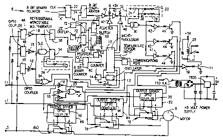
Figure 1 is a block circuit schem~tic drawing of the electrical circuit for
20 the controller of the invention;
Figure 2 is a block circuit schematic for a prefelred embodiment of the
controller conn~cted to an e~ al m~gn~tic contactor and motor;
Figure 3 is a circuit schem~tic for the output driver shown in Fig. 1; and
Figure 4 is a logic flow chart for software according to the invention for
25 the microprocessor shown in Fig. 1.
DESC}~TPTION OF THE PREFERRED EMBODIMENT
The present invention comprises a controller, generally design~te l by
reft;lence number 8, having a microprocessor 10 for operating motors 9 at
WO 95/02920 PCT/US94/07894
~ 8 ~ ~
more energy-efficient and hence more economical rates. The controller 8
embodiment described here is for a three-phase AC induction motor 9 that is
to be used with an external contactor.
While the controller 8 is described here by refelellce to the ~lcfelled
S embodiment, it will be readily understood that numerous mo~ e~tions and
subs~itutions could be made without departing from the invention. For
example, the components could be hardwiled in.~te~(l of using printed circuit
boards (PCB's). Similarly, components and their relative arrangements may
be varied.
The microprocessor 10 may take any of the various known forms, so
long as it contains an internal program that monitors the phase relationship of
voltage and ~;ulr~llL inputs and retards or advances trigger impulses used to
control SCR's that in turn make n~cess~ry phase rel~tion~hir adjustments.
Voltage and ~;ullelll phase relationships can continuously change and hence to
provnde power for efficient operation this phase relationship needs to be
readjusted ~uLo~ tir~lly as applied merh~nic~l loads and line voltages vary.
While the controller 8 embodiment described here is for a three-phase
motor, those skilled in the art will readily understand the design of a
comparable controller for one or two-phase motor operation.
The internal program may be devised in numerous dirrerellL forms and
modes so long as it contains the logic steps set forth in Figure 4, in the order
giverl.
Shown in Figure 1 is the microprocessor 10 that is co~n~cte~l to an
oscillator 12 cont~ining a 12-megaHertz clock used for the central processor
unit (CPU) clock. A counter 14 serves to enable the clock cont~in~-l in
oscillator 12 to function as a clock for other coulllers as described below.
Current signals from each of the three phases, L1, L2 and L3 (see
Figure 1), for the motor 9 are input to AC input opto couplers 96 that are
conn~cteA across output SCR modules, 76, 78, and 80. The AC input opto
wo gs/02920 2 t 6 ~ 2 PCTIUS94/07894
couplers 96 are used to detect the zero crossing of each of three phases. The
three ;UllC;llt signals are each shaped by Schmitt trigger Cil~;UilS 18 and then
sent to NOR gate 20. The output of NOR gate 20 is sent to an 8 bit binary
counter 22, for which the clock in oscillator 12, as divided by 2048 in counter
5 14, serves as a clock signal. As soon as the phase ~;ulrenl output from NOR
gate 20 drops to zero, counter 22 begins to count and send its outpu~ to digital8 bit colll~alator 24.
So long as the phase cuilen~ are not zero, the output of NOR gate 20
will be at the high level and the counter 22 will be brought into a reset state.Once the NOR gate 20 output becomes zero and the output of the
counter 22 passes to the comparator 24, it acts to co~ ale this information withthe motor's ~iullelll fire delay value obtained from register 28. This register
28 stores the ~;ullelll fire delay value which the microprocessor 10 calc~ te-l
based on the mr~llred motor power factor input when operation of the
15 controller 8 was initi~trtl, as ~ cll~se-l in detail below. The microprocessor 10,
using mr~llrements of zero cros~ing~ for the voltage and ~ullenl, refers to a
look-up table in an intPrn~l read only memory (ROM) to detell~ ,e the amount
of time delay required to effectively retard gating signals. Data stored in the
internal ROM is so determinP~l as to identify actual llltim~te full load power
20 factors for the motor 9 being controlled. Such ~etçrmin~ti-~ns are made usingtechni-lues known to those skilled in the art. The col.l~a,alor 24 thelefole
co~ aLes the output of running cuulllel 22 with the fixed value of the
CalClll~te~l ~;Ull`elll fire delay value stored in register 28. When the output of
counter 22 is less than the output of register 28, the signal from comparator 2425 is zero. After the outputs of counter 22 and register 28 equalize the digitalcolll~arator 24 uul~uls a positive signal that is applied to a pulse generator 32
implemente~l by a Schmitt NAND gate 30. The pulse generator 32 includes an
oscillator circuit having a capacitor 34, two i~lentir~l but oppositely connrcte-l
signal rectifier diodes 36 and two resistors 38 and 39, resistor 38 being of
WO 95/02920 PCT/US94/07894
4 ;~
approximately four times the value of resistor 39. Open drain il~ el~ 40 are
used as a wire OR circuit to handle "picket fencing" of motor 9 operation and
allow the microprocessor to control the motor 9 by gating SCR pulses. The
output of the pulse generator 32 is split and ~imlllt~neously passed through
S three drivers 42. The identical signals from the drivers 42 then each pass to
Darlington transistors 44 used to .simlllt~n~ously fire gates of co..es~onding
SCR's through the output drivers 82, 84 and 86.
Zero voltage crossing values for the three power phases are ~letecte(1
using three AC input opto couplers 48 conn~cte~l in a wye configuration. The
10 opto couplers 48 isolate the controller 8, for safety reasons, from e~lt;lllal
voltages. After passage through Schmitt triggers 18 where the signals are
shaped, the ~ul~uLs of Schmitt triggers 18 are passed to AND gate 52. The
output of AND gate 52 is three times the AC input frequency and is applied to
the input of a retriggerable monostable multi-vibrator 54 having a time co~l
15 determinP!-l by resistor and capacitor 56. The retriggerable monostable multi-
vibrator 54 is chosen to catch any power phase loss into the controller 8 input.In combination with resistor and capacitor 56 the monostable multi-vibrator 54
acts to effect illl~llu~Lion when any one or more of the power phases is not
opera~ing. A second retriggerable monostable multi-vibrator 58 is conn~cte~l
20 directly to the output of one of the ~chmitt triggers 18 from its opto coupler 48
and serves to indicate the exact time when the phase of the voltage input, in
this case power phase 1, crosses the zero level. At that time a short pulse fromdual retriggerable monostable multi-vibrator 58 resets counter 60 to
immediately commence counting from 0. The clock of oscillator 12, being
25 divided by 2048 through counter 14, acts as the clock for counter 60. If the
ullellL for the power phase conn~ctecl to the phase 1 input drops to zero, the
signal from the output of AND gate 52 write the counter 60 value into register
62 and an external inlell~L from NOR gate 64 is issued. This value is used
wo 95,02g20 ~ 1 ~ 6 8 6 2 PCT/US94/07894
as il~lmation data by the progr~rnme(l microprocessor 10 and is read from
register 62 through a common data bus 63.
When the controller 8 is set or reset, the required power factor for the
connected motor is input using dual inline package (DIP) digital switches 66
5 that are then read through buffer 68. The first of eight switches for digital
switch 66 is conn~cte~l to a selecte~l soft start operation; the next three are used
to set the soft-start ramp time; and the rem~inin~ switches are connPctç~l to
input the m~ lred power factor for a fully loaded motor. This power factor
must be dete. ~ 1 by the operator using a power factor meter, as are hlown
10 in the art, and input before i~ g operation of the conkoller 8.
In operation the controller calculates the percen~ge of energy savings
and displays these values on multi-segment LED displays 72 that are driven by
decoder-drivers 74. When a fault is ~etçctç~l, the LED displays 72 flash, e.g.,
all "8"'s, to alert the operator.
Turning to Figure 2, it shows the controller 8 in a typical in.ct~ tion
with an in~llr,tion motor 9, e~Lelnal m~netic contactor 118, and the control
circuit for the contactor 120. The contacts of relay 29 of the controller 8 are
intended to be wired to the control circuit 120 of the e~ ~l m~netic
contactor 118. When the controller 8 is functioning properly and no faults are
~letectecl, the microprocessor 10 oul~u~ a signal to driver 19 eller~ lg relay
29, closing its contacts allowing the motor 9 to be turned on. If a fault is
~letçcte~l, the contacts of relay 19 will open and the motor will be turned off.If power is detçcte~l on input ~ al Ll, L2 or L3 before relay 29 is
energized, the controller 8 will not turn on.
The SCR modules are generally l~Çelcllced by numbers 76, 78 and 80,
for each of the three power phases. Each SCR module 76, 78 and 80 is
respectively connected to one of the output drivers 82, 84 and 86 which are
i~le.ntir.~l and are detailed in figure 3.
WO 95/02920 2 ~ , PCT/US94/07894
.
Figure 3 shows the electrical circuit schematic for each of the three SCR
driver cil~iuiL~ 82, 84 and 86, which are all identical. In this circuit a pulsetransformer 90 is provided a signal through resistor 92 from its Darlington
drive ll~sislor 44. Rectifier diode 94 is provided for su~,ession.
S As also shown in Figure 3, the output from one of the pulse ll~r~"ller
90's secondaries passes through serially connecte(l resistor 98 and rectifier
diode 100 into the gate of the SCR. The negative gate voltage is clamped by
the diode 102, across the secondary winding. Terminal 1 is conn~cte~l to the
gate of the SCR and terminal 2 is conn~cte~l to the cathode of the SCR. The
output of the other pulse l~ xro~ller 90 secondary passes through serially
conn~ctç~l rectifier diode 106 and resistor 104 into the gate of the other SCR
of the pair. The negative gate voltage is clamped by the diode 108 across the
secondary winding. Terminal 4 is col-l~kcle(l to the gate of the SCR and
~al 3 is connPct~l to the cathode of the SCR. Con~ ctiQn between the
cathode and gate is n~etl~l to trigger SCR firing. A metal oxide varistor 110
is conn~cte~l across the power le~ of the SCR's, which can be Thyristors,
for surge su~ression and a resistor 112 and capacitor 114 are also connected
across the SCR's in a conventional manner to stabilize their operation (Dv/Dt
S~ ,ession).
The light emit~in diode (LED) side of AC input opto coupler 96 is
conn~cte l across the power l~""i..~l~ of the SCR's in series with resistor 97.
When the SCR's are on, there is no cu~ l flowing through the LEDs and the
output tran~istor of the opto coupler 96 is off. When the SCR's are off, cullellL
flows through resistor 97 and the LEDs of the opto coupler 96 turn the output
25 transistor on.
Figure 4, is self explanatory to those knowledgeable in the art. It sets
forth logic of the algo,ill~,l, used for microprocessor 10.
As can be seen, the controller 8 of this invention is ~lesign~l so that its
microprocessor 10 ~erates without e~le~lal memory in an essentially four-port
WO 95/02920 PCT/US94107894
2 7 66862
configuration. One port operates as a data bus for input-output peripherals.
Another port is a control bus to access peripheral integrated cir~;uiL~. Anotherport serves as the input for phase voltage and ~;ullelll me~llrements, and
temperature data from a controller heat sink, while the last of the ports has the
S ~llxili~ry function of providing input to external hltell~Ls and a serial link.
In the described plef~lled embo-liment the microprocessor 10 is an
INTEL 8051.
As will be readily a~parellL, many mo(life~tions of this invention can be
made by those skilled in the art without departing from its spirit and scope. It10 is intended therefore that the invention should be limite~l only by the appended
claims.