Note: Descriptions are shown in the official language in which they were submitted.
~1~7~27
METHOD AND APPARATUS FOR INCREASING ANTENNA EFFICIENCY
FOR HAND-HELD MOBILE SATELLITE COMMUNICATIONS TERMINAL
FIELD OF THE Ihv~NllON:
This invention relates generally to ant~n~A~ and, in
particular, to four arm helical spiral antPnn~.
BACKGROUND OF THE INVENTION:
One conventional antenna type is known as a four arm
helical spiral, wherein transmit and receive antenna
~ elements may be interleaved with one another. This type of
antenna provides a generally hemispherical coverage region.
As a result, and if such an antenna type were to be
employed as an antenna for a user terminal in a satellite
communication system, in particular a non-geosynchronous
orbit satellite communication system, the gain for low
satellite elevation angles is greater than for a satellite
that is directly overhead, thus compensating to some degree
~or the greater path loss to a satellite near the horizon.
However, one disadvantage of conventional four arm helical
spiral antennas is that they tend to be physically larger
than is customary for hand-held user terminals, such as
cellular telephones. A second disadvantage is that loss
between the active elements and the ant~n~s tends to be
greater than desirable. A further disadvantage is an
undesirable loss that can result from mutual coupling
between interleaved transmit and receive antenna elements.
- ~ 2~67~2~
Docket No.:LQ-95026 2
OBJECTS OF THE INVENTION:
It is a first object of this invention to provide an
improved antenna structure that overcomes the foregoing and
other disadvantages.
A second object of this invention is to provide a four arm
helical spiral antenna structure having a reduced size and
a reduced loss, rela~ive to conventional antenna
structures.
A third object of this invention is to provide an
interleaved helical spiral antenna structure wherein the
transmit and receive antenna elements or radiators are
width and thus impedance modulated, and wherein the line
widths of transmit radiators are aligned with the line
widths of adjacent receive radiators so as to m;n;m;ze
coupling therebetween.
A further object of this invention is to provide a helical
spiral antenna structure having a construction that
provides an optimum placement of radiators, amplifiers,
filters, and hybrid couplers, that maximizes thermal and
electrical isolation between high power transmit amplifiers
and lower power receive amplifiers, and that furthermore
places all of these components above a rotary antenna
joint, thereby reducing losses.
SUMMARY OF THE INVENTION
The foregoing and other problems are overcome and the
objects of the invention are realized by an antenna
structure that includes a plurality of transmit linear
elements arranged parallel to one another and a plurality
of receive linear elements arranged parallel to one
another. Individual ones of the plurality of transmit
~ 7 ~ 2 ~
Docket No.:LQ-95026 3
linear elements are spaced apart from one another and have
one of the plurality of receive linear elements disposed
therebetween. In accordance with this invention a width of
each of the plurality of transmit linear elements and the
plurality of receive linear elements varies periodically
along a length of the linear element, thereby also
periodically impedance modulating each element.
Furthermore, a narrowest width portion of a transmit linear
element is disposed adjacent to a widest width portion of
lo an adjacently disposed receive linear element, and vice
versa, thereby minimizing coupling between the elements.
In accordance with a further aspect of this invention the
transmit amplifiers and associated componen~s, and the
receive amplifiers and associated components, are located
at opposite ends of an antenna stalk such that transmit
amplifiers and receive amplifiers are intimately associated
with their respective antenna elements, thereby further
~;";m; zing losses. Also, because the transmit amplifiers
may generate considerable heat, the construction technique
thermally isolates the lower power receive amplifiers from
the higher power transmit amplifiers. Also, the transmit
amplifiers are preferably located at the end of the antenna
stalk that is nearest to the user transceiver, thereby
providing improved heat sinking.
A further aspect of this invention employs active impedance
matching between the antenna elements and their respective
amplifiers to maximize the coupling of energy from the
radiating elements to and from their associated amplifiers.
Impedance matching also occurs in bandpass filters which
are preferably embodied as multi-disk resonators. Also, the
radiating line width is selected to minimize the need for
impedance transformation between the amplifiers and free
space.
~ ~67427
Docket No.:LQ-95026 4
BRIEF DESCRIPTION OF THE DRAWINGS
The above set forth and other features of the invention are
made more apparent in the ensuing Detailed Description of
the Invention when read in conjunction with the attached
Drawings, wherein:
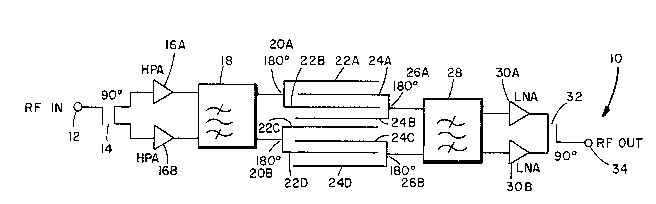
Fig. 1 is a block diagram of an antenna system in
accordance with this invention;
Fig. 2A is a representative diagram of the antenna system
of Fig. l;
Fig. 2B is a simplified illustration of a user terminal
antenna structure in accordance with this invention;
Fig. 3 shows an enlarged portion of the interleaved
transmit and receive antenna elements of Figs. 2A and 2B
and illustrates the width modulation, and consequent
impedance modulation, in accordance with an aspect of this
invention; and
Fig. 4 is a block diagram of a satellite communication
system of a type within which the antenna system of this
invention finds utility.
DETAILED DESCRIPTION OF THE INVENTION
Reference is made to Figs. 1, 2A, 2B and 3 for the ensuing
description of a presently preferred embodiment of this
invention.
In Fig. 1 an RF input signal is applied ~o an input node 12
of an antenna system 10. The input node 12 is connected to
a 90~ hybrid 14 which provides a first input to a first
high power amplifier (HPA) 16a and a quadrature input to a
~16~27
.
Docket No.:LQ-95026 5
second HPA 16b. The HPA 16a and 16b are poWer amplifiers
suitable for amplifying the RF input signal to a level
sufficient for driving the transmit antenna. In a preferred
embodiment of this invention the HPAs 16a and 16b are
embodied within monolithic microwave integra~ed circuits
(MMICs) of small size. The outputs of the HPAs 16a and 16b
(offset by 90~ from one another) are applied to a bandpass
filter 18 and thence to 180C hybrids 2Oa and 2Ob. The
hybrids 20a and 20b have outputs (offset by 180~ from one
a~other) connected to individual ones of the ~our arms or
radiators, also referred to herein as elements 22a-22d, of
the transmit antenna. Due the operation of the hybrids 14,
20a ~nd 20b the RF signals in each arm are o~fset by 90~
from one another (i.e., in quadrature).
The receiving portion of the antenna 10 includes a four arm
receive antenna having elements 24a-24d which are
interleaved with the transmit elements 22a-22d as shown
most clearly in Fig. 2A. The interleaved transmit and
receive elements are spiral wound about a dielectric
circular cylindrical form or tube 36 which forms the body
of the antenna 10 (Fig. 2B). The transmit and receive
elements are also width modulated as shown in Fig. 3 so as
to reduce losses due to mutual coupling. This aspect of
the invention is described in further detail below.
Continuing with the description of the bloc~ diagram in
Fig. 1, the quadrature outputs of the receive elements 24a-
24d are coupled via 180~ hybrids 26a and 26b to a bandpass
filter 28. The output of the bandpass filter 28 feeds the
inputs of a first low noise amplifier (LNA) 30a and a
second LNA 3Ob. The LNAs 3Oa and 3Ob are also preferably
embodied within MMICs. The outputs of the LNAs 3Oa and 3Ob
are coupled, via a go~ hybrid 32, to an RF output node 34.
In a presently preferred embodiment of the invention the
-
2~67~2~
.
Doc~et No.:LQ-95026 6
antenna system lo of Fig. 1 forms a portion of a hand held
user terminal 9a as depicted in Fig. 4. As such, it should
be realized that the RF input signal that is applied to the
input node 12 is derived at least in part from a user's
voice input signal. In like manner, the RF output signal
from the node 34 is applied to mixers and a demodulator for
extracting signalling information and for also deriving an
audio signal for the user. The various circuits within the
hand held user terminal sa that perform these f~nctions are
lo not germane to an understanding of this invention and are
not described in further detail. It should be realized
that the hand held user terminal sa is but one suitable
application for the antenna 10 of this invention, and is
not to be construed in a limiting sense upon the
application of, and uses for, the antenna 10 of this
invention.
As shown in Fig. 3, the antenna elements are width
modulated along substantially their entire length. For
those regions where the width is the widest the impedance
is the lowest, while conversely where the width is the
narrowest the impedance is the highest. The elements are
thus width modulated to periodically transform their
impedance. When the elements are at higher impedance
(narrower~ the voltage is higher, and when the elements are
wider, the impedance is lower and the voltage is also
lower. By aligning the element widths on ~he transmit
radia~ors 22a-22d to be wide adjacent to the element widths
on the receive radiators 24a-24d which are narrow the
coupling is minimized.
Also, in a preferred embodiment of this invention pairs of
radiators are formed as electrically conductive layers on
opposite sides of a flexible printed circuit board which
forms the dielectric circular cylindrical form or tube 36
of Fig. 2B. This tends to further reduce coupling, while
,
~ 6742~
Docket No.:LQ-95026 7
facilitating the interconnections as shown. Alternate
radiators are connected by the 180~ hybrids 20a, 20b, 26a,
26b which are coupled, preferably, to disc-type resonators
which form the filters 18 and 28 in quadrature, thereby
providing the desired circular polarizations.
To reiterate, and as is illustrated most clearly in Figs.
2A and 3, the transmit and receive antenna radiators or
elements 22a-22d and 24a-24d, respectively, are interleaved
lo with one another and are offset such that the high
impedance portion of a transmit element is adjacent to the
low impedance portion of receive element, and vice versa.
A first aspect of this invention thus inter-weaves transmit
and receive ant~nn~, and also shapes the radiating lines
to m;n;r;ze losses due to mutual coupling, while also
shortening the length required for efficient reception.
In a presently preferred em~odiment of this invention,
wherein the transmit frequencies are in the L-~and and the
receive frequencies are in the S-band, the elements are
width modulated so as to provide approximately an
approximately 10 ohm minimum impedance and a maximum
impedance in the range of approximately 200 ohms to
approximately 300 ohms. The number of periods of width
modulation is at least one, while a preferred number is a
function of length (e.g., eight to ten inches). A most
desired period is sized to one-half wavelength so that in
an established standing wave the current ~;mllm is
achieved where the impedance is lowest and the voltage
maximum is achieved where the impedance is highest.
However, in the general case the transmit and receive
frequencies are different and thus have different
wavelengths. As such, it can be realized that some
compromise may be necessary in order to adjust the antenna
modulation period as a function of the difference between
2t 6'7427
Docket No.:LQ-sso26 8
the transmit and receive wavelengths.
A second aspect of this inventiOn, shown in Fig. 2B, feeds
the transmit antenna and the receive antenna from opposite
ends of the antenna stalk so that the transmit HPAs 16a and
16b, and the recei~e LNAs 3Oa and 3Ob, are intimately
associated with their respective antenna elements, thereby
further m;n;m;zing losses. Also, because the HPAs 16a and
16b may generate considerable heat, the construction
t~hnique illustrated in Fig. 2B thermally isolates the
LNAs 30a and 30b from the HPAs 16a and 16b.
A further aspect of this invention employs active impedance
matching between the antenna elements and their respective
amplifiers to r~x;mi ze the coupling of energy from the
radiating elements ~o and from their associated amplifiers.
Impedance matching also occurs in the filters 18 and 28.
Also, the radiating line width is selected to minimize the
need for impedance transformation between the amplifiers
and free space.
For example, power FETs (a component of the transmitter
HPAs 16a and 16b) have a characteristically low output
impedance. As a result, line widths connected to the
outputs of the HPAs 16a and 16b are preferably made wide
- (for example, 10 ohms or less). Conversely, the input
impedance of the LNAs 3Oa and 3Ob is characteristically
high. As a result, the line widths connected to the inputs
of LNAs 30a and 30b is made wider (for example, up to 200
ohms) at the input junction point.
As is best seen in Figs. 2A and 2B, two four arm helical
spirals are formed by wrapping the width modulated lines
around the low loss dielectric tube 36. The tube 36 is
preferably formed from a flexible printed circuit board
substrate on which the antenna element conductors are
2~g7~2~
Docket No.:LQ-95026 9
- disposed, and which also mounts certain other of the
components, such as the hybrids 2Oa, 2Ob, 26a and 26b. A
suitable thickness for the wall of the tube 36 is 0.0625",
and a suitable diameter is 0.6". In the example described
herein, the transmit frequency (L-band) is lower than the
receive frequency (S-band) and the transmit elements 22a-
22d are therefore physically larger than the receive
elements 24a-24d.
The HPAs 16a and 16b are located at the base of the tube 36
which is adjacent to the body of the hand-held user
terminal 9a (Fig. 4). This arrangement provides the thermal
mass and radiator surface required to dissipate heat
generated by the HPAs 16a and 16b.
The LNAs 3Oa and 3Ob are located at the top of the tube 36,
and are thus thermally isolated from the HPAs 16a and 16b.
Both the HPAs and the LNAs are preferably embodied within
M~ICs, and as a result have a very small size, thereby
facilitating their incorporation within the antenna stalk
itself.
It should further be noted that the HPAs, LNAs, filters and
hybrids of the antenna system 10 are preferably all located
above a conventional rotary joint 38 that connects the
antenna stalk to the user terminal 9a. As a result, it is
not necessary to feed the HPA-amplified RF signals through
the rotary joint 38, nor is it necessary to feed a received
but unamplified signal through the joint. Placing all major
components of the antenna system 10 above the rotary joint
38, within the antenna stalk itself, thus improves the
overall operation of the user terminal and significantly
reduces losses.
The two LNAs 3Oa, 3Ob and the two HPAs 16a, 16b are used to
both couple and to provide a low loss active match to the
~ 2~67~2~
Docket No.:LQ-95026 10
antenna impedances. The impedance of the 180~llybrid 18 is
preferably selected to ma~ch to the output ;~r~nce of the
HPAs 16a and 16b and the antenna radiator ;m~ nce.
A cable 40 is used to bring the output from the LNAs 3Oa,
3Ob to the receiver electronics and to provide bias
potentials to the LNAs. The cables 40 also brings the
transmitter signal to the HPAs for final amplification and
the received signals to subsequent receiver stages. The
cable passes through aper~ures 36a and 36b in the center of
the disc resonators forming the filters 18 and 28. The
center of the disc resonators have no field and, as a
result, the proximity of the cable 40 does not
significantly affect their microwave performance.
Having described in detail the presently preferred
lS embodiment of this invention, reference is now ~ade to Fig.
4 for illustrating a block diagram of a satellite
communications system of a type to which the antenna 10 of
this invention can be applied. In the satellite
~o~ml~nications system a constellation of low earth orbit
satellites la enables users to make phone calls anywhere in
the world.
More particularly, Fig. 4 illustrates a satellite
transponder lb configured for full duplex communication.
The communications payload includes one or more such
transponders having a plurality of an~nn~ 2 to receive
signals from the earth~s surface, low noise amplifiers 3,
frequency shifters or converters 4 comprised of a local
oscillator and a mixer, followed by amplifiers 5, high
power amplifiers 6 and transmitting antennas 7. Filters 8
are also included to pass desired in-band signals and
reject unwanted out-of-band noise signals. One transponder
receives signals from the antenna 10 of a user terminal 9a,
frequency shifts the received user signals, and transmits
~, 2~67~27
Docket No.:LQ-95026 11
the frequency shifted signals to a ground station, such as
a gateway sb that is connected to the pu~lic switched
telephone network (PSTN). A second transponder receives
signals from one or more of the gateways 9b, frequency
shifts the received signals, and transmits the frequency
shifted signals to the antenna 10 of the user terminal gb.
In this manner a full duplex communication path (voice
and/or data) can be established between user terminals 9a
and terminals connected ~o the PSTN.
In a presently preferred embodiment of this i~lvention the
user terminals 9a (fixed or mobile) are capable of
operating in a full duplex mode and communicate via, by
example, L-band RF links (uplink) and S-band RF links
(downlink) through the return and forward satellite
transponders, respectively. Uplink L-band RF links may
operate within a frequency range of 1.61 GHz to 1.626 GHz,
bandwidth 16.5 MHz, and are pre~erably modulated with voice
signals and/or digital signals in accordance with a spread
spectrum technique. Downlink S-band RF links may operate
within a frequency range of 2.4835 GHz to 2.5 G~z,
bandwidth 16.5 MHz. The gateway sb may communicate with the
satellite la via receive antenna 2b and transmit antenna 7a
with, by example, a full duplex C-band RF link that may
operate within a range of frequencies centered on 5 G~z.
The C-band RF links bi-directionally convey communication
feeder links, and also convey satellite commands (forward
link) and receive telemetry information (return link). The
L-~and and the S-band satellite antennas 2a and 7b,
respectively, are multiple beam (preferably 16 beam)
antennas that provide earth coverage within an associated
service region. Two or more satellites la may each convey
the same communication ~etween a given user terminal 9a and
one of the gateways sb by the use of spread spectrum
techniques. This mode of operation thus provides for
diversity combining at the respective receivers, leading to
.
~ 2~7427
Docket No.:LQ-95026 12
an increased resistance to fading and facilitating the
implementation of a soft handoff procedure.
It is pointed out that all of the frequencies, bandwidths
and the like that are described above are representative of
but one particular system. Other frequencies and bands of
frequencies may be used with no change in the principles
being discussed. Furthermore, the various antenna-related
dimensions, numbers of elements, couplers, filters and
amplifiers, radiator impedances and the like that have been
described above are illustrative, and are not to be
cons~rued in a limiting sense upon the practice of this
invention.
Thus, while the invention has been particularly shown and
described with respect to preferred embodiments thereof, it
will be understood by those s~illed in the art that changes
in form and details may be made therein without departing
from the scope and spirit of the invention.
-