Note: Descriptions are shown in the official language in which they were submitted.
2 ~ ~ l'~46
dv/dt LIMITING OF INVERTER OUTPUT VOLTAGE
BACKGROUND AND SUMMARY OF THE INVENTION
This invention relates generally to inverter-driven induction motor
systems and, more particularly, to a dv/dt limiting circuit for controlling
the rate
of rise of inverter output voltage.
Adjustable frequency drives for controlling the speed of an
induction motor are well known. Such drives often comprise a static inverter
for converting a direct current (dc) input signal into an alternating current
(ac)
output signal having a frequency controllable by the user. These inverters may
be of several types, one common type including power switching elements
such as insulated gate bipolar transistors (IGBTs) gated by firing signals
from
a pulse width modulator.
However, such IGBT-based inverters generate rise rates in output
voltage reaching up to 15,000 volts/N sec. This shows up at the motor input
as a high peak voltage, due in part to impedance mismatch between the motor
and cable, combined with long cables connecting the motor and drive. While
this may have a negligible effect at very short cable lengths, on relatively
long
cables the PWM pulses can act as impulse waves on the motor cable resulting
in reflection phenomena. This can cause the peak voltage at the motor, to
approach a theoretical limit of two times. Such high peak voltages and the
associated currents caused by high rise rates can have detrimental effects on
the motor such as causing bearing failure or a failure in the motor windings.
Large peak voltages occurring repeatedly over the cycle of the PWM waveform
create stresses on the insulation of the motor stator winding. Also, a high
frequency "ringing" waveform appears at the front and rear of each pulse,
contributing to transient voltage amplitudes.
The dv/dt limiting circuit of the present invention addresses this
problem by controlling inverter output to limit voltage rise rates to between
500
and 1500 volts/N sec. This rise rate is low enough to allow reasonably long
cabling between the inverter and motor without introducing the high peak
voltages that would otherwise be introduced by the distributed inductance and
capacitance inherent in the cable.
216754b
-2-
The present circuit is coupled between the inverter and motor and
includes three capacitors connected in a delta configuration with each node
connected between an inductor and a diode bridge rectifier input. Outputs
from the bridge rectifier are passed through a resistor/capacitor circuit to
return
trapped energy to the inverter do bus and to control peak output voltage. A
large do capacitor stores trapped inductor energy when an output contactor is
opened.
These and other features and advantages of the present
invention will become apparent upon review of the following specification
taken
in conjunction with the accompanying drawings.
BRIEF DESCRIPTION OF THE DRAWINGS
Figure 1 is a schematic illustration of the limiting circuit of the
present invention, as implemented in a typical application.
Figure 2 is a more detailed view of a portion of the present
limiting circuit.
Figure 3 graphically illustrates the voltage prior to the motor cable
with and without the circuit of the present invention.
Figure 4 is a graph similar to Figure 3 showing the voltage
applied to the controlled motor.
DETAILED DESCRIPTION OF THE PREFERRED EMBODIMENT
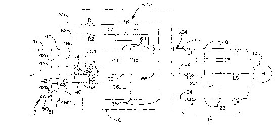
Turning now to the drawings and in particular to Figure 1, the
limiting circuit of the present invention is indicated generally at 10.
Circuit 10
is connected between an inverter 12 and an ac induction motor 14 adapted to
operate on a load (not shown). Circuit 10 is electrically connected to motor
14
by a conductive cable 16. The distributed capacitances and inductances of
cable 16 are modeled as capacitors C1, C2 and C3 connected in a delta
configuration between series connected inductors L1 and L4 at node 18,
between L2 and L5 at node 20 and between L3 and L6 at node 22. Cable 16
is connected to circuit 10 output contactor 24 via modeled lines 30, 32, 34.
216546
-3-
The inputs to limiting circuit 10 are provided from output lines 36,
38 and 40 of inverter 12. These inverter output lines are connected to
limiting
circuit input lines 54, 56 and 58, respectively. Inverter output line 36 is
connected to inverter line 42 intermediate a pair of switches 42a and 42b.
Inverter outputs 38 and 40 are connected in a similar fashion to inverter
lines
44 and 46, respectively. Switches 42a, 44a, 46a, 42b, 44b, 46b are preferably
power switching elements such as insulated gate bipolar transistors (IGBTs)
which are alternately switched on and off by firing signals from a separately
connected element such as a micro-processor based pulse width modulator
(not shown). A do voltage is supplied across bus lines 48 and 50 via a voltage
source 52. Inverter 12 is thus adapted to convert do power applied by power
supply 52 to polyphase alternating current necessary to power motor 14.
If limiting circuit 10 were not included, inverter output lines 36, 38,
40 would be directly coupled to cable lines 30, 32, 34. However, this
conventional configuration has several inherent disadvantages, the most
notable of which is a high voltage rise rate and peak voltage to the
distributed
capacitances and inductances of cable 16, as modeled in Figure 1. This not
only adversely affects motor 14 but also limits the length of cable 16.
Limiting circuit 10 counteracts such effects and raises cable
length limits by limiting the rate of rise of voltage at the cable input and
clamping positive voltage levels and returning trapped energy back onto do
bus lines 48 and 50. Circuit 10 receives inputs on lines 54, 56 and 58 from
inverter outputs 36, 38 and 40. Circuit 10 also includes output lines 60 and
62
connected to inverter 12 at nodes 44a and 44b, or the junctions at which line
44 joins bus lines 48 and 50, respectively. Input signals received on input
lines 54, 56, 58 are passed in series through a corresponding inductor L7, L8,
L9. Inductor L7 is connected at node 64 to parallel capacitors C4 and C5.
Inductor L8 is connected at node 66 to parallel capacitors C4 and C6 and L9
at node 68 to C6 and C5, capacitors C4, C5 and C6 being connected in a
delta configuration.
Each of nodes 64, 66, 68 is electrically connected to an output
of a fast recovery three-phase diode bridge rectifier 70. Rectifier 70
produces
2 ~ ~~'~46
-4-
do output signals to lines 60 and 62 and therefore connected nodes 49 and 51.
Lines 60 and 62 each include a resistor, R1 and R2 respectively, having a
capacitor C7 connected therebetween. Figure 2 illustrates limiting circuit 10,
and in particular rectifier 70, in additional detail. As shown therein the
input
to rectifier 70 comes from nodes 64, 66 and 68 with capacitors C4, C5 and C6
connected therebetween. Node 64 is electrically coupled to line 72 through
diode D1 and to line 74 through diode D2. Similarly, node 66 connects to line
72 through diode D3 and to line 74 through diode D4. Finally, node 68 is
coupled to line 72 through diode D5 and to line 74 through diode D6. Lines
72 and 74 provide do current to resistors R1 and R2 with capacitor C7
connected therebetween.
Capacitor C7 preferably includes a set of three capacitors C7,,
C72, and C73 interconnected as shown in Figure 2. Capacitor C7,, in this
exemplary embodiment, preferably having a capacitance of about 0.1
microfarads provides a path for high frequency currents, thus controlling the
peak voltage which is clamped by the capacitors and rectifier bridge.
Capacitors C72 and C73 are electrolytic capacitors which do not have the high
frequency characteristics necessary to allow operation absent C7, but which,
in series, have a voltage rating higher than can be normally attained with a
single commercially available capacitor. The capacitances of C72 and C73,
about 120 microfarads in this exemplary embodiment, are preferably chosen
so as to allow motor current flowing through inductors L7, L8 and L9 to be
absorbed when output contactor 24 is suddenly opened. If these capacitors
are not properly sized, the voltage at the output of rectifier 70 would
increase
to a point wherein diodes D1-D6 may fail.
Referring now to Figure 3, the voltage at cable 16 is plotted with
respect to time. Curve 80 represents the voltage which would be seen directly
from inverter 12, without the benefit of limiting circuit 10. Curve 82
conversely
shows the voltage output from limiting circuit 10. Curve 80 includes three
main
segments, an increasing segment 80a, a peak 80b and a leveled off portion
80c. As illustrated in the figure, curve segment 80a has a fairly steep slope,
indicative of a sharp voltage rise rate, up to and exceeding 15,000 volts/N
sec.
21 ~~'~46
-5-
It is apparent, however, that the slope of segment 82a
corresponding to the signal as conditioned by limiting circuit 10, is much
more
gradual, reduced to only 500 to 1500 voIts/N sec. Curve 82, though, has a
peak voltage 82b slightly above that of 80b, due to the voltage drop in R1 and
R2 causing the voltage on C7 to exceed the do bus voltage 52, but then levels
off after a brief oscillation at 82c to voltage 82d.
Figure 4 plots the voltage applied to motor 14, further taking into
consideration the distributed capacitances and inductances inherent in cable
16. Curve 84 illustrates this voltage without benefit of limiting circuit 10
and
curve 86 with circuit 10. As shown therein curve 86 substantially mirrors
curve
84 but on a more gradual and narrower scale. While voltage peaks at point
84b, after a sharp increase along curve portion 84a, at up to twice the
inverter
voltage, the peak voltage at 86b is only slightly more than one times the
inverter voltage. In addition, the applied voltage is more stable.
Thus, the present limiting circuit reduces the risk of detrimental
high voltage peaks and rise rates to an inverter-driven induction motor. The
circuit is simple, inexpensive and readily implemented in existing motor/drive
systems.
For the sake of clarity, the values of the electrical components
used in one exemplary embodiment of the present invention were omitted from
Figure 1. For completeness, they are included herebelow for limiting voltage
rise rated to 500 voIts/N sec in a 20 horsepower motor, the values of
capacitors C1-C3 and inductors L1-L6 being dependent upon the length and
electrical characteristics of cable 16. However, it should be readily apparent
to one of skill in the art that these component values will change with
horsepower and the desired voltage rise rate limit.
21~15~6
-6-
Resistors Capacitors fncluctors Diodes
R1 20iZ C4 10,OOOpFL7 130~crH D1 BY329-1200
R2 2012 C5 10,OOOpFL8 130~uH D2 BY329-1200
(R1 and C6 10,OOOpFL9 130NH D3 BY329-1200
R2 are C7, .1NF D4 BY329-1200
100 Watt) C7z 120NF D5 BY329-1200
C73 120~uF D6 BY329-1200
The foregoing discussion discloses and describes an exemplary
embodiment of the present invention. One skilled in the art will readily
recognize from such discussion, and from the accompanying drawings and
appended claims, that certain changes, modifications and variations can be
made therein without departing from the spirit and scope of the present
invention as defined in the following claims.