Note: Descriptions are shown in the official language in which they were submitted.
~O 9~I10084 216 8 3 3 5 pCT~s94/11273
--
-1-
VIRTUAL ADDRESSING BUFFER CIRCUIT
Background of the Invention
Field of the Invention
The present invention relates to the field of
translation look-a-side buffers, and, more particularly,
it relates to the ability to translate a given input
address to a user specified address location.
Description of the Related Art
A standard translation look-a-side buffer of the
prior art enables a user to transfer an address request
from a central processing unit (CPU) to an alternative
address location in the system memory. The basic
operation of a translation look-a-side buffer entails
comparing an input address to a stored address to verify
if the two addresses match each other. If no match has
occurred, the input address is transferred through the
buffer and is output to the system bus without
modification. If a match occurs, the input address is
replaced with a stored output address which is
transferred to the system bus to replace the input
address.
The operation of translation look-a-side buffers of
the prior art is limited to a direct translation of an
input memory location to a specified output memory
location. The translation look-a-side buffer must
compare the entire input address with the entire stored
address in order to determine if an address translation
is to occur. In addition, the translation look-a-side
buffer must replace the entire input address with a new
output address. These two requirements have greatly
limited the number of possible applications of the
translation look-a-side buffer. The look-a-side buffer,
is only useful in .those applications where it is
desirable to directly translate one address location to
a new address location.
~16~335
'CVO 95!10084 PCT/US94111273
-2-
In order to provide improved memory system
optimization, a need exists for a more flexible memory
translation circuit that masks out certain bits from the
input address which may be irrelevant to the comparison
with the stored address before determining if the address '
translation is to occur. In addition, it is desirable to
isolate certain portions of the input address that remain
unchanged when the address translation occurs.
Summary of the Invention
The present invention is a virtual addressing buffer
circuit which provides improved address mapping
flexibility over the traditional translation look-a-side
buffers of the prior art . The preferred embodiment of
the virtual addressing buffer circuit comprises a
filtering and verification portion, a formatting portion,
a translation portion and a command portion. The
filtering and verification portion compares the input
address to a stored match address, after filtering out
any address bits which are not relevant to the
determination of whether the two addresses match. The
formatting portion generates an output address as a
combination of bits from a translated address and from
the original input address as determined by a user
specified format. The translation portion determines if
the formatted address or if the input address is output
from the virtual addressing buffer. The ability to
format the output address enables the user to replace
certain bits of the input address with the corresponding
bits from the translated address without requiring that
the entire input address be replaced.
A preferred embodiment of the filtering and
verification portion of the virtual addressing buffer
comprises a 32-bit filtering and comparison circuit; a
match register which stores a match address; and a
filtering register which stores,a filtering address that
indicates the bit positions of the input address which
WO 95!10084 2 ~ 6 g 3 3 5 PCT/US94/11273
-3-
are not to be considered in the comparison of the input
address to the stored match address. The bit pattern in
the filtering register is not fixed, so any bit location
in the input address can be masked out of the comparison
before the address is verified. In a preferred
embodiment of the virtual addressing buffer, each bit of
the match address is compared with each bit of the input
address. The output of the comparison is logically ORed
with a corresponding bit of the filtering address to
enable certain bits which have a don't care condition to
be masked out of the address comparison. The output of
the 32-bit filtering comparison circuit includes a_ HIT
signal, an active high signal, which indicates if the
filtered input address matches the stored match address.
If the filtered input address matches the stored match
address, the HIT signal is active. If the filtered input
address does not match the address stored in the match
register, the HIT signal is inactive.
The format portion of the virtual addressing buffer
circuit operates in parallel with the filtering portion.
In a preferred embodiment, the format portion comprises
thirty-two 2x1 multiplexers; a translate register which
stores a translated address; and a format register which
indicates which bits of an output address are to be from
the translated address and which bits are to remain the
same as the input address. In a preferred embodiment of
the virtual addressing buffer circuit, each bit of the
input address is connected to a first input of one of the
2x1 multiplexers, and a corresponding bit of the
translate register is connected to a second input of one
of the thirty-two 2x1 multiplexers. The select line of
each of the 2x1 multiplexers is connected to the
corresponding bit of the format register which selects .
between an input address bit and a translated address bit
for output from the virtual addressing buffer circuit .
If the corresponding format bit at the select line is at
- VO 95/10084 ~ PCT/US9411127, 3 ,
-4-
a logic low level, the translated address bit is output
from the multiplexes. If the corresponding format bit is
at an inactive level, the input address is output from
the multiplexes. The outputs of each of the thirty-two
2x1 multiplexers are combined to form a formatted output
address.
The translation portion of the virtual addressing
buffer selects between the input address and the
formatted output address for output from the virtual
addressing buffer circuit depending on the condition of
the HIT signal. In a preferred embodiment, the
translation portion comprises a 32-bit 2x1 multiplexes.
A first input of the multiplexes is connected to the
input address and a second input is connected to the
formatted output address. The select line of the
multiplexes is connected to the HIT signal which
determines which address is output from the virtual
addressing buffer. If the HIT signal is at an active
level, indicating that the filtered input address matches
the stored match address, the formatted output address is
selected for output from the virtual addressing buffer.
If the HIT signal is at an inactive level, indicating
that the filtered input address does not match the stored
match address, the original input address is selected for
output from the virtual addressing buffer circuit without
alteration.
In addition to the address manipulation features
described above, the command portion of the virtual
addressing buffer circuit controls the output of several
command signals to external circuits to indicate how the
circuitry external to the virtual addressing buffer
should respond to the address output from the virtual
addressing buffer. The command signals, all of which are
active high signals are an ignore signal, a terminate
signal, and a bypass signal. A preset condition of each
of these signals are stored in a command register. The
_ WO 9/10084 ~ 16 ~ 3 3 5 PCT~S94/11273 I
-5-
preset conditions of the command signals are ANDed with
the HIT signal and are therefore output from the virtual
addressing buffer at an active level only when the HIT
signal is active. The ignore signal is used to inform a
slow downstream bus to ignore the address from the
virtual addressing buffer circuit and enables a device on
a faster local bus to respond to the address request.
The bypass signal is used to block the faster local bus
from responding to the address from the virtual
'addressing buffer circuit and lets the slower downstream
bus respond to the address request. The terminate signal .
is used for more complex responses to address requests,
such as the emulation of devices that are not physically
present. The detection of the terminate command by a bus
controller causes the controller to send an end of cycle
command back to the CPU that requested the address of the
emulated device and enables an emulation routine to
respond to the address request.
In a preferred embodiment of a dual comparison.
virtual addressing buffer, two virtual addressing buffers
are formed in one integrated circuit whereby two address
comparisons and redirections are performed
contemporaneously. In a preferred embodiment, a first
32-bit filtering comparison circuit is connected to an
input address, a first match address and a first
filtering address. The first filtering address masks out
those address bits which are not important to the first
address comparison. A second 32-bit filtering comparison
circuit is connected to the same input address, a second
match address and a second filtering address. The second
filtering address masks out a different set of address
bits which are not important to the second address
comparison. An output of the first 32-bit comparison .
circuit is a HITO signal which is an active high signal.
The HITO signal indicates when the first filtered input
address is equivalent to the first match address. An
O 95/10084 216 8 3 3 5 pCT~S94111273
T
-6-
output of the second 32-bit filtering comparison circuit
is a HIT1 signal which is an active high signal. The
HIT1 signal indicates when the second filtered input '
address is equivalent to the second match address.
Contemporaneously with the address comparisons, two
formatted output addresses are generated. A first set of
thirty-two single-bit multiplexers is used to create a
first formatted output address from the bits of the input
address and from a first lookup address. A select input
of each multiplexes is connected to a bit from a first
format address which determines if a bit from the input
address or from the first lookup address should be used
to form the f first formatted output address . A second set
of thirty-two single-bit multiplexers is used to create
a second formatted output address from the bits of the
input address and from a second lookup address. A select
input of each multiplexes is connected to a bit from a
second format address which determines if a bit from the
input address or from the second lookup address should be
used to form the second formatted output address. Outputs
of the first thirty-two multiplexers are combined to form
a first formatted output address. Outputs of the second
thirty-two multiplexers are combined to form a second
formatted output address.
The first formatted output address and the second
formatted output address are connected to a first 32-bit
2x1 multiplexes. The HITO signal is connected to a
select line of the first multiplexes and is used to
select between the first formatted output address and the
second formatted output address for output as a final
formatted output address. If the HITO signal is at an
active level, the first formatted output address is
selected for output as the final formatted output
address. If the HITO.signal is at an inactive level, the
second formatted output address is selected for output.
The use of the HITO signal as the select signal for the
216 8 3 3 5 pCT~S941i 1273
first 32-bit multiplexer indicates that the first
formatted output address has priority over the second
formatted output address. Thus, if the HITl signal and
the HITO signal are both active, indicating that a match
was made with both filtered input addresses, then the
first formatted output address is selected for output
over the second formatted output address.
In a preferred embodiment, the HITO signal and the
HIT1 signal are each connected to a two-input OR gate to
determine if a match occurred between either of the
stored input addresses and the filtered input address to
determine the translated address which is output from the
dual comparison virtual addressing buffer circuit. The
input address and the final formatted output address are
connected to a second 32-bit 2x1 multiplexer. An output
of the OR gate is inverted by an inverter and then
connected to a select line of the second 32-bit 2x1
multiplexer. If neither the HITO signal nor the HITl
signal are active, then the filtered input address did
not match either of the stored match addresses and the
input address is selected for output as the translated
memory address without alteration. If either the HITO
signal or the HITl signal is active, then a match
occurred between one of the filtered input addresses and
one or more of the stored match addresses, and the final
formatted output address is selected for output as the
translated memory address. Thus, the dual comparison
virtual addressing buffer completes the two address
comparisons and redirections in approximately the same
time that it took to complete the single comparison
virtual addressing buffer circuit to complete a single
comparison.
Several common programming procedures can be .
improved using either the single or double comparison
embodiments of the virtual addressing buffer. First,
"paged system BIOS shadowing" can be improved by enabling
CA 02168335 1999-08-25
_8_
the most frequently accessed code from the system BIOS to be
copied from the relatively slow access ROM storage to the local
memory of the high-speed processor. After the BIOS is copied to
the local memory, the virtual addressing buffer is used to
redirect the data requests from the slow downstream BIOS to the
faster local memory where the BIOS commands are now stored.
Second, to better utilize the existing physical of memory
blocks which are reserved by the CPU for applications which are
not in use.
Third, program debugging, I/O trapping and device emulation
can be enhanced using the terminate features of the virtual
addressing buffer circuit.
Therefore, various aspects of the invention are provided as
follows
A virtual addressing buffer circuit wherein an input
address is translated into an output address, said virtual
addressing buffer circuit comprises:
a filtering and verification portion for comparing a
stored match address to an input address and for filtering
out any bits of the input address which are not relevant to
a determination of whether the input address matches the
stored match address;
a formatting portion for generating a formatted output
address from a translated address and from said input
address; and
a translation portion for selecting between said input
address and said formatted output address for output as said
output address.
A method of translating an input address to a
translated output address comprising the steps of:
comparing a stored match address to said input address;
filtering out any bits of said address comparison which
are not relevant to a determination of whether the input
CA 02168335 2001-10-10
8a
address is to be translated;
generating a formatted output address from the
bits of a translated address and said input address;
and
selecting between said input address and said
formatted output address for output as said
translated output address depending on the result of
the address comparison between said stored match
address and said input address.
A method of utilizing a physical memory of a
computer system which is larger than the logical memory
space of a CPU by enabling the use of memory blocks which
are above the logical memory space of a CPU, comprising
the steps of:
configuring the system memory map to include a
memory space above the logic memory space of the
CPU;
filtering out any bits of a CPU requested address
which are not relevant to a determination of whether
the CPU requested address matches the stored match
address;
comparing the resultant filtered CPU requested
address to a stored match address to determine
whether the CPU requested address is located above
the logical memory space on the CPU;
formatting an output: address from a translated
address and from said CPtT requested address; and
selecting between said CPU requested address
and said formatted output address for output as said
output address based upon the results of the
comparison of said resultant filtered CPU requested
address to a stored match address.
These and other features and advantages of the
CA 02168335 2001-10-10
8b
present invention are set forth more completely in the
accompanying drawings and the following description.
Brief Description of the Drawings
Figure 1 is a schematic diagram of a preferred
embodiment of the virtual addressing buffer circuit of
the present invention.
Figure 2 is a more detailed block diagram of
the virtual addressing buffer circuit in combination with
a central processing unit and with a local bus controller
of a host computer system.
WO 95,/10084 ~ ~ PCT/US94I11273
_g_
Detailed Description of the Preferred Embodiments
The present invention is a virtual addressing buffer
circuit which provides improved address mapping
flexibility for memory system optimization. Figure 1
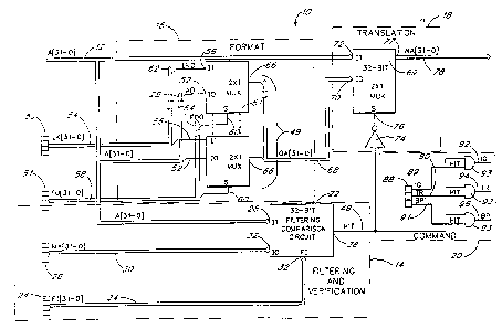
illustrates a preferred embodiment of a 32-bit virtual
addressing buffer circuit 10. The virtual addressing
buffer circuit 10 performs a number of operations on an
input address A[31-0] on a bus 12 to determine if the
input address A[31-0] is to be translated to a new
address, if at all.
The preferred embodiment of the virtual addressing
buffer circuit 10 comprises a filtering and verification
portion 14, a format portion 16, a translation portion 18
and a command portion 20. A brief description of each of
these portions follows, while a more detailed description
is provided below. The filtering and verification
portion 14 compares an input address to a stored match
address and determines if the corresponding bits (i.e.,
the bits in the same bit position) of the two addresses
are equivalent. Next, the filtering and verification
portion 14 filters out some of the bits from the address
comparison whose values do not matter in the
determination of whether the input address is to be
translated or not. Lastly, the filtering and
verification portion 14 outputs a signal to indicate if
a match of the relevant bits has occurred. The format
portion 16 creates a formatted output address which is a
combination of bits from the input address A [31-O] and
from a stored translation address. The translation
portion 18 selects which address is to be output from the
virtual addressing buffer circuit 10 depending upon
whether the filtering and verification portion 14 detects
a match or not . If a match is detected, the formatted
output address is output from the virtual addressing
buffer circuit 10. If a match is not detected, the
original input address A[31-O] is output from the virtual
w
WO 95/10084 ~ ~ 6 8 3 3 5 PCT/US94/112,73
-10-
addressing buffer circuit 10 without alteration. The
command portion 20 outputs a series of command signals
which indicate the manner in which the external logic -
should respond to the translated address which is output
from the virtual addressing buffer circuit 10 of the
present invention.
As indicated in Figure 1, the filtering and
verification portion 14 of the virtual addressing buffer
circuit comprises a 32-bit filtering comparison circuit
.22; a filtering register 24 which stores a filtering
address FI[31-0]; and a match register 26 which stores a
match address MA[31-0]. The input address A[31-0] on the .
bus 12 is connected to an I1 input 28 of the filtering
comparison circuit 22. The match address MA[31-0] on a
bus 30 is connected to an IO input 32 of the filtering
comparison circuit 22. The filtering address FI [31-0] on
a bus 34 is connected to an FI input 36 of the filtering
comparison circuit 22. In a preferred embodiment, each
address bit of the input address A[31-0] on the bus 12 is
compared to a respective address bit of the stored match
address MA[31-0] on the bus 30 to determine whether the
address bits match. The match output for each bit will
be a logical one if a match occurs. This bit comparison
has the effect of an exclusive-NOR function represented
by a XNOR gate 40 in Figure 5 for bit 0. As illustrated
in Figure 5, the inputs of the representative XOR gate 40
are an AO bit on a line 41 and a MAO bit on a line 42,
and the output of the XOR gate 40 is a match output
signal, MATCHO, on a line 43, which is active high when
the inputs match. The match output is logically ORed
with a respective bit of the filtering address FI[31-0]
to mask out the unimportant address bits from effecting
the output of the address verification. This function is
illustrated in Figure 5 by an OR gate 44 whose inputs are
the MATCHO signal on the line 43 and the FIO bit on line
45. An output of the OR gate 44 is a BITOHIT signal on
WO 95110084 ~ ~ ~ PCT/US94/11273
-11-
a line 46, which indicates that bit 0 of the input
address matches bit 0 of the match address, or bit 0 has
been filtered out of the address data comparison. The
address bits of the input address A[31-0] whose values
must match the stored match address MA[31-0] for an
address translation to occur are indicated by storing a
logic low value (i.e., a zero), at the corresponding bit .
location in the filtering register 24. The address bits
of the input address A[31-0] whose values do not need to
match the stored match address for an address translation
to occur (i.e., those address bits that have a don't care
condition), are indicated by storing a logic high value
(i.e., a one), at the corresponding bit location in the
filtering register 24. Each OR gate 44 with an address
comparison input of a don't care bit will be forced to a
logic high value at the output by the logic high value of
the filtering address bit regardless of the result of the
address comparison. On the other hand, if the respective
address bit compare (i.e., both are a logic one or both
are a logic zero), then the output of the OR gate 44 will
be a logic one irrespective of the filter bit. The
outputs of all the OR functions, such as the BITOHIT
signal on the line 46 of the exemplary circuit of Figure
5, are logically ANDed together to determine if all of
the relevant address bits of the input address A [31-0]
match the respective bits of the stored match address
MA[31-0] . If a match has occurred, an output 38 of the
filtering comparison circuit 22 is at a logic high level.
If a match did not occur, the output 38 of the filtering
comparison circuit 22 is at a logic low level. The
output 38 of the 32-bit filtering comparison circuit 22
is connected to a HIT signal on the line 48 which is an
active high signal (i.e., if the comparison is true, the
HIT signal 48 is at a logic high level). The HIT signal
on the line. 48 conveys the result of the address
comparison from the filtering and verification portion 14
WO 95/10084 216 ~ 3 3 5 P~~S94/1127,3
-12-
to the translation portion 18 and the command portion 20
of the virtual addressing buffer circuit 10.
As indicated in Figure 1, the format portion 16 of
the virtual addressing buffer circuit 10 operates in
parallel with the filtering and verification portion 14
to create a formatted output address OA[31-0]. In a
preferred embodiment, the format portion 16 comprises 32
single-bit 2x1 multiplexers 49, a translate or lookup
register 50 and a format register 51. The translate
register 50 stores a lookup address LK[31-0] which
indicates the desired translated address location. The
format register 51 stores a format address FO [31-0] which
comprises a series of bits that indicate which bits from
the original input address A[31-O] on the bus 12 are to
remain unchanged and which bits are replaced with the
corresponding bits from the lookup address LK[31-0]. If
an address bit is to be taken from the input address on
the bus 12, a logic high value, i.e, a one, is placed in
the corresponding bit location in the format register 51.
If an address bit is to be taken from the lookup address
LK[31-0], a logic low value (i.e., a zero), is placed in
the corresponding bit location in the format register 51.
The thirty-two single-bit 2x1 multiplexers 49 are
used to select each of the bits which form the formatted
output address OA[31-O] from the corresponding bits of
the, lookup address LK[31-0] and the input address A[31-
0]. Each bit of the input address A[31-0] on the bus 12
is connected to an IO input 52 of one of the thirty-two
single-bit 2x1 multiplexers 49. A corresponding bit of
the lookup address LK[31-O] on a bus 54 is connected to
an I1 input 56, of the corresponding single-bit 2x1
multiplexes 49. A corresponding bit of the format
address FO [31-O] on a bus 58 is connected to a select
input 60 of the corresponding single-bit 2x1 multiplexes
49. For example, the first input address bit AO 28 is
connected to the IO input 52 of a first 2x1 multiplexes
~'VO 95/10084 g ~ ~ ~ PCT'/US94/11273
-13-
61. A first lookup address bit LKO 62 is connected to
the I1 input 56 of the first 2x1 multiplexes 61. A first
format bit FOO 64 is connected to the select input 60 of
the first 2x1 multiplexes 61. This configuration is
repeated for the remaining bits of the input address
A [31-0] on the bus 12, the lookup address LK [31-0] on the
bus 54 and the format address FO[31-0] on the bus 58 for
each of the remaining multiplexers 49. If a given bit of
the format address FO [31-0] is at a logic low value ( i . a .
a logic zero), the address bit at the IO input 52 of the
single-bit 2x1 multiplexes 49, in this case the
corresponding bit from the input address A(31-0], are
sent to an output 66 of the multiplexes 49. If a given
bit of the format address FO [31-0] is at a logic high
value (i.e., a logic one), the address bit at the I1
input 56, in this case the corresponding bit of the
lookup address LK[31-0], will be sent to the output 66 of
the multiplexes 49. The outputs 66 of each of the
thirty-two single-bit multiplexers 49 are combined to
form a formatted output address OA[31-0] on a bus 68
which is delivered to the filtering and translation
portion 14 of the virtual addressing buffer circuit 10.
The translation portion 18 selects between the
input address A[31-O] on the bus 12 and the formatted
address output address OA[31-0] on the bus 68 for output
from the virtual addressing buffer circuit 10. The
translation portion 18 comprises a 32-bit 2x1 multiplexes
69. The 32-bit formatted output address OA [31-O] on the
bus 68 is routed.to an IO input 70 of the 32-bit 2x1
multiplexes 69. The original 32-bit input address A[31-
0] on the bus 12 is connected to an I1 input 72 of the
32-bit 2x1 multiplexes 69. The HIT signal 48, which is
generated by the filtering and verification portion 14 of
the virtual addressing buffer 10, is sent through an
inverter 74 to a select input 76 of the 2x1 multiplexes
69 to select which of the two 32-bit address are sent to
WO 95/10084 ~ ~ ~ PC1'/US94111273 I
-14-
an output 77 of the 2x1 multiplexer 69. The output 77 of
the 2x1 multiplexer 69 is connected to a translated
memory address NA[31-0] on a bus 78 which is output from .
the virtual addressing buffer circuit 10. If the HIT
signal on the line 48, is at an active level (i.e., the
relevant bits of the input address A[31-0] on the bus 12
are equivalent .to the corresponding bit of the match
address MA[31-0] on the bus 42), the signal at the select
input 76 of the multiplexer 69 is at a low logic level.
If the signal at the select input 76 of the multiplexer
is at a logic low level, the address at the IO input 70,
which in this case is the formatted output address OA [31-
0] on the bus 68, will be selected to be output as the
translated memory address NA [31-0] on the bus 78 . If~ the
HIT signal on the line 48 is inactive, the signal at the
select input 76 of the 32-bit multiplexer 69 will be at
a high logic level. If the signal at the select input 76
of the multiplexer 69 is at a high logic level, the
address at the I1 input 72, which in this case is the
original address A[31-0] on the bus 12, will be selected
to be output as the translated memory address NA[31-0] on
the bus 78 without alteration.
The command portion 20 outputs a series of command
signals which indicate the manner in which the external
logic should respond to the translated memory address
NA[31-O] on the bus 78 which is output from the virtual
addressing buffer circuit 10. The individual functions
of the command signals will be described in more detail
later; however, their communication with the circuitry of
the virtual addressing buffer circuit 10 is described
hereinafter. The preset values of the command signals
are stored in a command register 88. The preset command
signals are a preset ignore signal (IG~), a preset bypass
signal (BP~), and a preset terminate signal (TR~). The
preset command signals which are stored in the command
resister 88 are active high signals and are set to a
WO 95/10084 ~ 3 3 ~ PCT/US94/11273
-15-
predetermined value by the user. The command signals are
only output when the virtual addressing buffer circuit 10
has translated the input address A[31-0] to a new
translated address value and the external circuitry needs
to operate in a different manner in response to the
translated address. Therefore, the preset command
signals that are stored in the command register 88 are
ANDed with the HIT signal on the line 48 before they are
output from the virtual addressing buffer circuit 10 to
ensure that the command signals are only output at an
active level when the HIT signal on the line 48 is at an
active level. The IG~ signal on a line 89, the TRH
signal on a line 90, and the BP~ signal on a line 91 are
each connected to'a first input of a two input AND gate
93. A second input of each of the two input AND gates 93
is connected to the HIT signal on the line 48. The
outputs of each of the AND gates 45 are an ignore signal
(IG) on the line 92, a terminate signal (TR) on the line
94 and a bypass signal (BP) on the line 96. Each of the
command signals which are output from the virtual
addressing buffer circuit 10 are active high signals and
can only be output at an active level when the input
address A[31-0] on the bus 12, after filtering, matches
the stored match address MA[31-0] on the bus 30.
The virtual addressing buffer 10 is advantageous
over conventional translation look-a-side buffers, as
conventional translation look-a-side buffers only connect
a series of address bits to the translation look-a-side
buffer (i.e., the upper eight bits or the lower sixteen
bits of a 32-bit address), and do not enable any
filtering of the address beyond the selection of bits
which are connected to the buffer. The filtering and
verification portion 14 of the virtual addressing buffer
10 enables the masking of any of the thirty-two bits of
the input address 12, all thirty-two of which are
connected as inputs of the virtual addressing buffer
PCT'/US94/1127, 3
WO 95/10084 216 8 :~ ~ 5
-16-
circuit 10. Further, the virtual addressing buffer
circuit 10 enables each bit of .the translated memory
address NA [31-0] on the bus 78 to be selected from either
the input address A[31-0] on the bus 12 or from the look-
s up address LK[31-0] on the bus 52. The conventional
translation look-a-side buffers only enable the direct
mapping of an input address to an output address and do
not enable the advantageous selection of the bits of the
output address from both a translated address and from
the original input address.
Referring also to Figure 2, in a preferred
embodiment, the virtual addressing buffer circuit (VAB)
10 is used in combination with a CPU 80, a local CPU bus
82, a local memory bus 84 and a local bus controller 86
of an exemplary computer system. In this embodiment, the
virtual addressing buffer circuit 10 is used as a buffer
between the CPU 80 and the memory bus 84 to more
efficiently reroute CPU address requests within the host
computer system. The control of the virtual addressing
buffer 10 is not fixed, so the operation of the virtual
addressing buffer 10 can be altered by the CPU 80 at
anytime during the operation of the host computer system.
The virtual addressing buffer 10 intercepts a CPU
requested address on the local CPU bus 82. The CPU
requested address, also referred to as the input address
A[31-0], on the bus 12 is sent to the virtual addressing
buffer circuit 10 where the filtering and verification
portion 14, formatting portion 16, translation portion
18, and command portion 20 of the virtual addressing
buffer circuit 10, which have been described above,
determine whether the input address A[31-0] from the CPU
80 is to be redirected to a different memory location
before the address is sent to a downstream bus, such as
the local memory bus 84.
In addition, Figure 2 illustrates the communication
between the virtual addressing buffer 10 and a
WO 9S/10084 ~ ~ ~ PCT/US94/11273
-17-
configuration register, or CONFIG REG, 87 which stores
all of the operating parameters of the virtual addressing
buffer circuit 10. The configuration register 87 is a
contiguous block of data in local I/O memory which stores
~ the filtering register 24, the match register 26, the
lookup register 50, the format register 51 and the
command register 88.
In use, the virtual addressing buffer circuit 10
must be initialized before it becomes operable. During
the system boot and memory mapping operations, the host
computer system reserves a block of its local I/O memory
for the configuration register 87 and writes the starting
address of the I/O memory block into an index register to
which the CPU 80 has access. The CPU 80 does not need to
know ultimately where the configuration register 87 is
located in the local I/O memory; however, it must know
the location of the indexing register which holds the
starting address of the configuration register 87. In
order to initialize the virtual addressing buffer circuit
. 10, the CPU 80 must write the desired values for the
filtering register 24, the match register 26, the lookup
register 50, the format register 51 and the command
register 88 into the configuration register 87. Once the
values of the configuration register 87 have been
initialized, the virtual addressing buffer 10 becomes
operable.
After the virtual addressing buffer circuit l0 has
been initialized, the CPU 80 can alter any of the
register values stored in the configuration register 87
to modify the memory locations to which the CPU 80
requested addresses are mapped at any time during the
operation of the host system. For example, if a portion
of the system memory is only utilized during an '
initialization routine of the system software, the CPU 80
can alter the data stored in the command register 87 of
a virtual addressing buffer circuit 10 after the system
WO 95/10084
216 8 3 3 5 p~~S94/11273 I
-18-
initialization routine is complete to redirect certain
address requests to this now unused block of physical
memory. The ability of the virtual addressing buffer
circuit 10 to redirect address requests during the
operation of the system is advantageous over the
translation look-a-side buffers of the prior art. The
known translation look-a-side buffers are hardwired to
the system bus to articulate a specific type of address
translation which is unchangeable and is often defined
before the ultimate use of the computer is known. Thus,
the virtual addressing buffer circuit 10 is more flexible
than translation look-aside buffers of the prior art~and
provides for a more optimized use of the system's
physical'memory.
In a preferred embodiment as illustrated in Figure
2, the command signals (the ignore signal IG on the line
92 , the terminate signal on the line 94 and the bypass
signal BP on the line 96) are connected to the local bus
controller 86. The local bus controller 86 reads the
status of the command signals and generates the
appropriate signals to be delivered to the downstream bus
controllers. Each of the command signals are
necessitated by different system configurations and by
different applications of the virtual addressing buffers
10. As described above, the HIT signal on the line 48 is
output at an active level every time an input address
matches a stored address. When the HIT signal on the
line 88 is at an active level, it indicates that the
original input address on the bus 12 has been redirected
to a new address location somewhere within the system.
The ignore signal IG on the line 92, the terminate signal
TR on the line 94, and the bypass signal BP on the line
96 are preferably issued at an active level only when the
HIT signal on the line 48 is at an active level and the
values of the preset command signals (the IG~ signal on
the line 89, the TRH signal on the line 90 and the BPS
WO 95110084 PCT/US94/11273
~ 16~:~~5
-19-
signal on the line 91) are set to an active level. The
IG signal and the BP signal are advantageously used when
a computer system is simultaneously operating two similar
devices or is storing the same data at two different
locations on two different busses and one of the devices
must be prevented from responding to the address request .
Usually one of the devices is located on a local fast
bus, such as the local CPU bus 82 or the memory bus 84,
and the other device is located on a slower downstream
bus. The ignore signal IG is used to enable the device
on the local fast bus to respond to the memory request
and blocks the slower downstream bus from responding.
The bypass signal BP is used to enable the device on the
slower downstream bus to respond to the memory request
and blocks the device on the local fast bus from
responding. The terminate signal TR is active when the
virtual addressing buffer 10 is being used for device
emulation. In the device emulation case, the terminate
signal is sent back to the CPU 80 to end the current bus
cycle.
When the command signals are received by the bus
controller 86, the bus controller 86 re-routes the CPU
defined bus control and bus definition signals in
accordance with the status of the command signals. The
bus control and definition signals which are redirected
depending upon the status of the command signals at the
bus controller 86 are an address status output signal
(ADS*) on a line 98 which indicates that a valid address
request has been sent to the CPU bus 82, a memory I/O
signal (M/IO*) on a line 100 which indicates when the
requested address is located on memory or an I/O device,
a read/write signal (W/R*) on a line 102 which indicates
when the bus cycle is a read or write cycle, and a
data/code signal (D/C*) on a line 104 which indicates
when the information that is to be retrieved is data or
an operation code.
WO 95/10084 PCT/US94/11273
2168:35
-20-
For example, in a typical use of the virtual
addressing buffer circuit 10, the CPU requested address
A[31-0] on the bus 12 is input to the virtual addressing
buffer circuit 10 after the completion of operations of
the filtering and verification portion 14 (Figure 1), the
formatting portion 16 (Figure 1), the translation portion
18 (Figure 1), and the command portion 20 (Figure 1), the
HIT signal 48 is issued at an active level to indicate
that the original input address A[31-0] is being
redirected to a translated memory address NA[31-0] on the
' bus 78. If the translated memory address NA[31-O] on the
bus 78 is located on a downstream bus, the bus control
and bus definition signals are modified by the local bus
controller 86 as needed and are passed to the downstream
bus along the following signal lines. The ADS* signal is
passed downstream as the MADS* signal on the line 106.
The M/IO* signal is passed downstream as the MM/IO*
signal on the line 108. The W/R* signal is passed
downstream as the MW/R* signal on the line 110. The D/C*
signal is passed downstream as the MD/C* signal on the
line 112. If the translated address NA[31-0] is located
on the local CPU bus 82, the ADS* signal on the line 98,
the M/IO* signal on the line 100, the W/R* signal on the
line 102 and the D/C* signal on the line 104 are
maintained on the local CPU bus 82 without alteration and
the requested device responds to the CPU 80 using
standard handshaking and termination procedures.
In a particularly preferred application of the
present system, addresses signals A[0] and A[1] are not
typical address signals, rather they are used to
differentiate the four bytes in a 32-bit word.
Typically, the four bytes are controlled by four byte
select lines BE [0] , BE [1] , BE [2] and BE [3] (not shown)
which are communicated to the device being accessed in
place of A[0] and A[1] . Thus, A[O] and A[1] are
available for other uses. The present invention takes
.- JVO 95/10084 ~ ~ ~ PCT/US94111273
-21-
advantage of the availability of the A [1] and A [0] lines
to enable the user to manipulate the W/R* and M/IO*
signals. Preferably, the W/R* and M/IO* signals are
delivered to the virtual addressing buffer circuit via
the A[1] signal line 102 and A[0] signal line 100,
respectively. The W/R* signal on the line 102 and M/IO*
signal on the line 100 are manipulated by the virtual
addressing buffer circuit 10 in the same manner as the
address signals and are output on the signal lines NA[1]
110 and NA[O] 108, respectively. In other embodiments,
if it is desirous to enable all thirty-two address signal
lines to carry 32-bits of addressing information,
additional lines can be added to the virtual addressing
buffer to enable the buffer to manipulate both the 32-
bits of addressing information, as well as the bus
definition signals such as the W/R* and M/IO* signals.
In another use of the virtual addressing buffer 10,
when the CPU requests an address A[31-O] on the bus 12,
the virtual addressing buffer circuit 10 reroutes the
input address A[31-0] to a translated memory address
NA[31-0] and outputs an ignore signal IG on the line 92
at an active level. When the ignore signal 92 is
received by the bus controller 86 at an active level, the
bus controller 86 generates a disable signal which
prevents the MADS* signal on the line 106, the MM/IO*
signal on the line 108, the MW/R* signal on the line 110
and the MD/C* signal on the line 112 from being
transmitted to a device on the slower downstream bus.
Instead, the ADS* signal on the line 98, the M/IO* signal
on the line 100, the W/R* signal on the line 102 and the
D/C* signal on the line 104 return to the local CPU bus
82 and enable a device on the faster CPU bus 82 to
respond to the translated memory address NA[31-0] on the
bus 78. Once~the translated memory address NA[31-0] is
received by the device on the local CPU bus 82, the
device on the local CPU bus 82 is responsible for
.- - WO 95/10084 ~ 16 ~ 3 3 ~ p~~s94/11273
-22-
responding to all of the bus handshaking requests and
issuing a RDY* signal on a line 114.to terminate the bus _
cycle, once it has delivered the requested data to a
local data bus 105.
~ In yet another example, when the CPU 80 requests an
address A[31-O] on the bus 12, the virtual addressing
buffer circuit 10 reroutes the input address A[31-0] to
a translated memory address NA[31-0] and outputs the
bypass signal BP on the line 92 at an active level. When
the bypass signal 92 is received by the bus controller 86
at an active level, the bus controller 86 generates a
disable signal and prevents the ADS* signal on the line
98, the M/IO* signal on the line 100, the W/R* signal on
the line 102, and the D/C* signal on the line 104 from
being delivered to the device on the local CPU bus 82.
Instead, the bus controller 86 modifies the bus control
and definition signals as needed and passes them onto the
downstream memory bus 84 along the following signal
lines. The ADS* signal is passed downstream as the MADS*
. signal on the line 106. The M/IO* signal is passed
downstream as the MM/IO* signal on the line 108. The
W/R* signal is passed downstream as the MW/R* signal on
the line 110. The D/C* signal is passed downstream as
the MD/C* signal on the line 112. The translated address
NA[31-0] on the bus 78 is passed onto the downstream bus
to address the desired device.
In a final example of the virtual addressing buffer
10, the terminate signal TR on the line 94 is issued when
the virtual addressing buffer 10 is used to emulate a
non-existent device. In a simple emulation example, the
virtual addressing buffer 10 translates the CPU requested
address A[31-OJ on the bus 12 to a translated address
NA[31-0] on the bus 78. The virtual addressing buffer 10
in turn outputs the terminate signal TR on the line 94 at
an active level which is sent to the local bus controller
86. The translated address NA[31-O] addresses a memory
WO 95/10084 ~ PCT/US94/11273
X168335
-23-
location that contains artificial data values which
emulate the data requested from the non-existent device.
The data stored at the translated memory location NA[31-
0] is placed on the local CPU bus 82 and is sent to the
CPU 80 in response to the data request. Upon receipt of
the terminate signal on the line 94, the local bus
controller 86 generates the RDY* signal on the line 114
which is sent to the CPU 80 indicating that valid data is
located on the local data bus 105. In a more complex
emulation example, the terminate signal TR on the line 94
causes the local bus controller 86 to generate a CPU
interrupt on a line 116 which causes an emulation routine
to be initiated, as will be described in more detail
below.
A single virtual addressing buffer 10 is only able
to detect and execute one address relocation at a given
time. Therefore, if multiple addresses need to be
relocated, more than one virtual addressing buffer 10
must be used. When multiple virtual addressing buffers
10 are used, it is preferable that the address
comparisons by the virtual addressing buffers 10 be
performed in parallel to prevent a long delay between the
local CPU bus 82 and the downstream busses. When
multiple virtual addressing buffers are used in parallel
as described above, the HIT signals of the individual
buffers 10 are used to select one of the multiple output
addresses and one set of the multiple command signals
from the outputs of the virtual addressing buffers which
is to be ultimately output to the downstream bus.
In a preferred embodiment of a dual comparison
virtual addressing buffer 200 illustrated in Figure 3,
two virtual addressing buffers 10 are formed in one
integrated circuit whereby two addresses comparisons and
redirections are performed contemporaneously. In a
preferred embodiment, a first 32-bit filtering comparison
circuit 202 is connected at an I1 input 204 to an input
r
i
WO 95/10084 ~ PCT/US94I11273
X168335
-24-
address A[31-O] on a bus 206 and at an IO input 208 to a
first mask address MAO [31-0] on a bus 210. A first FI
input 212 of the first 32-bit filtering comparison
circuit 202 is connected to a first filtering address
FIO[31-0] on a bus 214 to mask out those address bits
which are not important to the address comparison. In a
preferred embodiment, each address bit of the input
address A[31-0] on the bus 206 is compared to a
respective address bit of the first match address MAO [31-
O] on the bus 210 to determine whether the address bits
match. The match output for each bit will be a logical
one if a match occurs. As discussed above, this bit
comparison has the effect of an exclusive-NOR function
represented by a XNOR gate 40 in Figure 5 for bit 0. The
address bits of the input address A[31-0] on the bus 206
whose values must match the first match address MAO [31-0]
on the bus 210 for an address translation to occur are
indicated by a logic low value (i.e., a zero), at the
corresponding bit location in the first filtering address
FIO[31-O] on the bus 214. The address bits of the input
address A[31-0] on the bus 206 whose values do not need
to match the first match address MAO [31-0] on the bus 210
for an address translation to occur (i.e., those address
bits that have a don't care condition), are indicated by
2 5 a logic high value ( i . a . , a one ) , at the corresponding
bit location in the first filtering address FIO [31-0] .
Each OR gate 44 with an address comparison input of a
don't care bit will be forced to a logic high value at
the output by the logic high value of the filtering
address bit regardless of the address comparison. On the
other hand, if the respective address bit compare (i.e.,
both are a logic one or both are a logic zero), then the
output of the OR gate 44 will be a logic one irrespective ,
of the filter bit. 'The outputs of all of the OR
functions are logically ANDed together to determine if
all of the relevant address bits of the input address
'~O 95!10084
PCT/US94I11273
1 ~~:~3~
-25-
A[31-O] on the bus 206 match the respective bits of the
first match address MAO[31-0] on the bus 210. If a match
has occurred, an output 224 of the filtering comparison
circuit 202 is at a logic high level. If a match did not
occur, the output 224 of the filtering comparison circuit
202 is at a logic low level. The output 224 of the first
32-bit filtering comparison circuit 202 is connected to
a HITO signal on a line 226 which is an active high
signal. The HITO signal indicates when the relevant bits
of an input address A[31-0] on the bus 206 are equivalent
' to the corresponding bit of the first match address
MAO[31-0] on the bus 210. If the two addresses are
equivalent, the HITO signal on the line 226 is set to an
active level. If the two addresses are not equivalent,
the HITO on the line 226 is set to an inactive level.
In a preferred embodiment, a second 32-bit filtering
comparison circuit 230 is connected at an I1 input 232 to
the input address A[31-0] on the bus 206 and at an IO
input 234 to a second mask address MA1[31-0] on a bus
236. A FI input 238 of the second 32-bit filtering
comparison circuit 230 is connected to a second filtering
address FI1[31-0] on a bus 240 to mask out those address
bits which are not important to the address comparison.
The operation of the second filtering address comparison
circuit is 230 identical to the operation of the first
filtering comparison circuit 202 described above. An
output 250 of the second filtering comparison circuit 230
is connected to a HIT1 signal on a line 252 which is an
active high signal. The HIT1 signal indicates when the
relevant bits of an input address A[31-O] on the bus 206
are equivalent to the corresponding bit of the second
match address MA1[31-0] on the bus 236. If the two
addresses are equivalent, the HIT1 signal on the line 252
is set to an active level. If the two addresses are not
equivalent, the HIT1 signal on the line 252 is set to an
inactive level.
WO 95/10084 PCT/US94/11273
-26-
Contemporaneously with the address comparisons, two
formatted output addresses are prepared. A first set of
thirty-two single-bit multiplexers 254 are used to create
a first formatted output address OAO[31-0] from the bits
of the input address A[31-0] on the bus 206 and from the
first lookup address LKO[31-0] on the bus 256 depending
on the state of a select input 258 of the single-bit
multiplexers 254. The select input 258 of each
multiplexes 254 are connected to a respective bit from a
first format address FOO[31-O] on a bus 260. Respective
outputs 262 of the first thirty-two multiplexers 254 are
combined to form a first formatted output address OAO [31-
0] on a bus 264 which is a combination of address bits
from the input address A [31-0] on the bus 206 and the
first lookup address LKO[31-0] on the bus 256. A second
set of thirty-two single-bit multiplexers 266 are used to
select between a bit from the input address A [31-0] on
the bus 206 and a bit from a second lookup address
LK1[31-0] on a bus 268 depending on the state of a select
input 270 of each multiplexes 266. The select input 270
is connected to a bit from a second format address
FO1[31-0] on a bus 272. Each output 274 of the second
set of thirty-two multiplexers 266 are combined to form
a second formatted output address OA1[31-0] on a bus 276
which is a combination of the address bits from the input
address A[31-0] on the bus 206 and the second lookup
address LK1[31-0] on the bus 268.
The first output address OAO [31-0] on the bus 264 is
connected to an I1 input 278 of a first 32-bit 2x1
multiplexes 279 . A second output address OA1 [31-O] on
the bus 276 is connected to respective IO inputs 280 of
the first 32-bit 2x1 multiplexes 279. The HITO signal on
the line 226 is connected to a select line 281 of the
multiplexes 279 and is used to select between the first
formatted output address OAO [31-0] on the bus 264 and the
second formatted output address OAl[31-O] on the bus 276
'CVO 95110084 PCT/US94/11273
216335
-27-
for output as a final formatted output address OAF[31-0]
on a bus 282. If the HITO signal on the line 226 is at
an active level, indicating that the relevant bits of the
input address on the bus A[31-O] are equivalent to a
first match address MAO [31-0] on the bus 210, then the
first formatted output address OAO[31-0] on the bus 264
is selected for output as the final formatted output
address OAF[31-O] on the bus 282. If the HITO signal on
the line 226 is at an inactive level, two conditions
could have caused this to occur. Either, the relevant
bits of the input address A[31-0] on the bus 206 are
equivalent to the second match address MA1[31-Ol on the
bus 236 or neither of the match addresses MAO [31-O] or
MAl[31-O] matched the respective relevant bits of the
input addresses A[31-0]. In either case, the second
formatted output address OA1[31-0] on the bus 276 is
always selected for output because, in the case that
neither input address matches the stored match register,
it does not matter which formatted output address is
advanced as ultimately the original input address A[31-0]
on the bus 206 will be selected for the final output.
Using the configuration described in association with
Figure 1, the use of the HITO signal on the line 226 as
the select signal for the first 32-bit multiplexer 279
indicates that the first formatted output address OAO [31-
0] on the bus 264 has priority over the second formatted
output address OA1[31-0] on the bus 276. Thus, if the
HIT1 signal on the line 252 and the HITO signal on the
line 226 are both active, indicating that a match was
made with both filtered input addresses, then the first
formatted output address OAO [31-0] on the bus 264 will be
selected for output over the second formatted output
address OA1[31-0] on the bus 276, since the HITO signal
on the line 226 is chosen to control the select line 281
of the first 32-bit 2x1 multiplexer 279. The output of
WO 95/10084 216 8 3 3 5 p~~S94/11273
-28-
the first 32-bit 2x1 multiplexer 279 is advanced as the
final formatted output address OAF[.31-0] on the bus 282.
The HITO signal on the line 226 and the HIT1 signal
on the line 252, are each connected to an input of a two
s input NOR gate 286. An output 288 of the OR gate 286 is
inverted utilizing an inverter 289 before it is.sent to
a select line 290 of a second 32-bit 2x1 multiplexer 284.
An I1 input 292 of the second 32-bit 2x1 multiplexer 284
is connected to the input address A[31-0] on the bus 206.
An IO input 294 of the second 32-bit 2x1 multiplexes 284
is connected to the final formatted output address
OAF[31-0] on the bus 282. The select line 290 of the
second 32-bit multiplexes 284 selects between the final
formatted output address OAF [31-0] on the bus 282 and the
original input address A[31-0] on the bus 206. If
neither the HITO signal on the line 226 nor the HIT1
signal on the line 252 are active, then the filtered
input address did not match either of the stored match
addresses and the output of the OR gate 288 is a logic
low signal. The logic low signal is inverted by the
inverter 289, thus connecting a logic high signal to the
select line 290 of the second 32-bit 2x1 multiplexes 284,
causing the input address A [31-0] on the bus 206 which is
connected to the I1 input 292 of the multiplexes 284 to
be output as the translated memory address NA[31-0] on a
bus 296 without alteration. If either the HITO on the
line 226 or the HIT1 signal on the line 252 are active,
then a match occurred between one of the filtered input
address and one or more of the stored match addresses,
therefore the output of the OR gate 288 is an logic high
signal. The logic high signal is inverted by the
inverter 289 and therefore connects a logic low signal to
the select line 290 of the second 32-bit 2x1 multiplexes ,
284, causing the final formatted output address OAF [31-0]
294 which is connected to the IO input 294 of the second
WO 95/10084 PCT/US94/11273
16835
-29-
32-bit multiplexes 284 to be output as the translated
memory address NA[31-0] on the bus.296.
In addition to controlling the address output, the
dual comparison virtual addressing buffer circuit 200
also controls the output of the command signals for each
comparison. A first command register CMDO 298 stores a
first set of preset command signal values IGO~, TRO~ and
BPO ~ . A second command register CMD1 300 stores a second
set of preset command signal values IG1~, TR1~ and BP1~.
The first set of preset command signals is connected to
an Il input 302 of a 4-bit 2x1 multiplexes 304. The
second set of preset command signals is connected to'an
IO input 306 of the 4-bit 2x1 multiplexes 304. The
select input 308 of the multiplexes is connected to the
HITO signal on the line 226. If the HITO signal on the
line 226 is at an active level, indicating that the
relevant bits of the input address on the bus A[31-O] on
the bus 206 are equivalent to a first match address
MAO [31-0] on the bus 210; then the first set of preset
command signal values IGO~, TRO~ and BPO~ are output from
the multiplexes 304 to a bus 310. If the HITO signal on
the line 226 is at an inactive level, two conditions
could have caused this to occur. Either, the relevant
bits of the input address A[31-0] on the bus 206 are
equivalent to the second match address MA1[31-0] on the
bus 236 or neither of the match addresses MAO[31-0] or
MA1[31-O] matched the respective relevant bits of the
input addresses A[31-0]. In either case, the second set
of preset command signal values IG1~, TR1~ and BP1~ are
output from the multiplexes 304 to the bus 310. The use
of the HITO signal on the line 226 as the select signal
for the first 4-bit multiplexes 304 indicates that the
first set of preset command signals has priority over the
second set of preset command signals. Thus, if the HIT1
signal on the line 252 and the HITO signal on the line
226 are both active, indicating that a match was made
WO 95/10084 PCT/US94I11213
X168335
-30-
with the relevant bits of both match addresses, then the
first set of preset command signals will be selected for
output over the second set of preset command signals,
since the HITO signal on the line 226 is chosen to
control the select line of the first 4-bit 2x1
multiplexer 279.
In order to prevent the command signals from being
output at a logic high level from the dual comparison
virtual addressing buffer circuit 20 when an address
match did not occur, each of the preset command signals
is gated before it is output. Each of the preset command
signals which is an output of the first 4-bit 2x1
multiplexer 304 is connected to a first input 312 of a
respective two-input AND gate 314. A second input 316 of
the two-input AND gate 314 is connected to the output 288
of the of the OR gate 286. If neither the HITO signal on
the line 226 nor the HIT1 signal on the line 252 is
active, then the filtered input address did not match
either of the stored match addresses and the output of
the OR gate 288 is an logic low signal. A logic low
signal connected to the inputs 316 of the two-input AND
gates 314 will mask the preset values of the command
signals, and the outputs of the AND gates 314 will be
forced to logic low values regardless of the preset input
values. If either the HITO on the line 226 or the HIT1
signal on the line 252 is active, then a match occurred
between one of the filtered input address and one or more
of the stored match addresses. Therefore, the output of
the OR gate 288 is a logic high signal. A logic high
signal connected to the inputs 316 of the two-input AND
gates 314 will enable the preset values of the command
signals IG~, TRH and BP~ to pass through the AND gate 314
without alteration. Utilizing the dual comparison ,
virtual addressing buffer 200, the two address
comparisons, redirections and the control of the command
signals of the dual comparison embodiment are completed
WO9~/10084 216 (~ J 3'J p~~s94/11273
-31-
in approximately the same time period that it took to
complete the single comparison, redirection and control
of the command signals in the single comparison virtual
addressing buffer circuit embodiment 10.
Figure 4 illustrates the dual comparison virtual
addressing buffer circuit (DVAB) 200, as illustrated in
Figure 3, in communication with a CPU 400 in a host
computer system 401. The CPU 400 is also in
communication with an upgrade processor or a co-processor
(COP) 404 and a cache controller (CCH) 406 along a local
CPU BUS 402: In addition, the CPU 400 is in
communication with local memory 408, local video memory
410 and a local status buffer 411 along a local memory
bus, MEM~BUS, 412. The dual comparison virtual
addressing buffer 200 and a local bus arbitrator 414 are
located between the CPU BUS 402 and the MEM BUS 412 to
manage the address requests from the CPU 400. Further,
the MEM BUS 412 is in communication with a system bus,
SYSTEM-BUS, 416 via an axillary bus bridge 418. Lastly,
the system bus 416 is in communication with an internal
bus, INT BUS, 420 via an internal bus bridge 422 and an
external bus, EXT BUS 424, via a system bus bridge 426.
The external bus 424 is in communication with system
expansion cards 427 such as, external memory cards 428,
external network controller cards 430, and external video
controller cards 432. Typically, the external bus 424
utilizes a standard bus control format such as EISA or
ISA to control the communications with the expansion
cards 427. The internal bus 420 communicates with
integrated system elements such as BIOS ROM 434, an
internal video controller 436, an internal disk
controller 438 and a keyboard controller 440. The
internal bus 420 can use any system defined bus control
protocol known to one of skill in the art.
The dual comparison virtual addressing buffer 200
can be used to optimize the physical address space of the
WO 95/10084
PCT/US9-1/112?3
....
-32-
host a computer system 401 in a number of ways. Notably,
the dual comparison virtual addressing buffer 200 can be
used to implement "paged system BIOS shadowing" a
technique which is commonly used to increase processing
speeds. The BIOS shadowing feature enables the
frequently accessed code from the system BIOS to be
copied from the relatively slow access ROM storage 434 to
the local memory 408 of the high-speed CPU 400 in order
to increase the speed of BIOS address requests.
Typically, the BIOS addresses that are stored in the ROM
are compressed to enable all of the BIOS commands to be
stored in the small storage area of the ROM 434.
Therefore, in order to copy the BIOS commands, the paged
addresses are decompressed and stored in the local memory
408. In addition, the locations in the local memory 408
where the BIOS commands are stored are write protected to
prevent the BIOS commands from being corrupted.
In one example, the entire contents of the system
BIOS ROM 434 is decoded and copied from the ROM 434 on
the INT BUS 420 to local memory 408 on the local memory
bus 410.. As is well known in the art, the ROM addresses
are advantageously stored in a paged format to reduce the
address space required to access each of the BIOS
commands. In use, as the CPU 80 requests one of the
paged BIOS addresses, a first portion of the dual
comparison virtual addressing buffer 200 will redirect
the requested address to the correct page location in the
local memory 408. A first match address MAO[31-0] is
used to redirect a first BIOS paged access request from
the slow downstream BIOS 434 to the appropriate page
location in the local memory 408 where the BIOS commands
are now stored. A second match address MA1[31-0] is used
to terminate all write accesses to the addresses in local ,
memory 408 where the BIOS commands are stored. When a
write request is received by the dual comparison virtual
addressing buffer 200 which matches the write protected
WO 95110084
PCT/US94/11273
."".,. .
-33-
addresses of the second match address MA1[31-0], the dual
comparison virtual addressing buffer 200 will issue an
ignore command which will indicate to the local bus
controller 414 to ignore the write request (W/R*) to
prevent access to the protected local memory area 408.
As described above, the W/R* and M/IO* signals are
altered by the virtual addressing buffer circuit via the
A [1J and A [0] input lines, respectively.
In order to implement paged BIOS shadowing using
conventional translation look-a-side buffers, an
individual translation look-a-side buffer would have to
be provided for each page of addresses of the BIOS ROM
434 that are redirected to the local memory 408. In the
case of a 128KB BIOS ROM 434 which is paged in 16KB
pages, eight conventional translation look-a-side buffers
would be required to redirect the addresses of the eight
pages of commands which are stored in the ROM 434 and
additional control logic would be required to block the
write lines from being transmitted to the ROM locations
434 in the local memory 408. A similar sized BIOS ROM
434 can be converted to local memory 408 using the dual
comparison virtual addressing buffer 200 as described
above.
Secondly, to better utilize the existing physical
memory, "memory ranged blanking" can be overcome to
reclaim physical memory addresses which are blanked out
by the CPU in order to address external devices.
Typically, in a DOS compatible system certain logical
address locations are reserved for accessing memory
mapped external devices. The corresponding physical
memory locations to these memory mapped addresses are
unused as their address must be reserved to access the
external devices. Therefore, blocks of the physical
memory are wasted because their addresses are reserved
for the access of memory mapped external devices. To
enable the use of the wasted physical memory space which
WO 95110084 PCT/US94111273
- 2168335
-34-
is reserved to access external devices, a first portion
of the dual comparison virtual addressing buffer 200 can
be used to direct address requests for the reserved
memory mapped space to the downstream bus where the
requested external device is located. In addition, the
system memory is configured at start-up such that the CPU
400 is informed that a block of memory the size of the
blanked out memory mapped space exists over and above the
physical memory space. A second portion of the virtual
addressing buffer 200 redirects the memory requests for
memory locations above the physical address space to the
physical memory space which was blocked from direct
access by the first portion of the dual virtual
addressing buffer 200.
For example, in a DOS compatible system, a 1MB
address space between 15MB and 16MB is reserved for an
external network controller card 430. If a 32MB physical
memory space is available, the CPU 400 is informed that
a 33MB memory is available for access. A first portion
of the dual virtual addressing buffer 200, is used to
send any address requests in the 15MB to 16MB range to
the slower downstream external bus 424 where the network
controller card 430 is located. The first portion of the
dual virtual addressing buffer 200 generates a bypass
signal BP when the CPU requested address matches any of
the addresses in the 15MB to 16MB address range to inform
the local CPU BUS 402 to bypass the local memory bus 412
and to pass the addresses along with the bus definition
and control signals onto the slower downstream EXT BUS
424 where the network controller card 430 is located. A
second portion of the dual virtual addressing buffer 200
is used to translate the CPU addresses requests in the
32MB to 33MB range to the physical address space in the
15MB to 16MB range which is being unused. The second
portion of the dual virtual addressing buffer 200 will
generate an ignore signal to inform the downstream
WO 95/10084 216 ~ ~ ~ ~ P~~s94111273
-35-
EXT BUS 428 to ignore the redirected address requesting
the 15MB to 16MB range to prevent~the external network
controller card 430 at the 15MB to 16MB memory-mapped
address location from answering the request and thereby
~ enabling the local memory 408 at the 15MB to 16MB range
to respond.
Advantageously, by utilizing the dual virtual
addressing buffer embodiment 200 for each block of
physical memory space which is blocked from use by memory
mapped external device such as video devices 436, disk
drive devices 438, network devices 430, etc., the memory
space can be remapped for use by the CPU 400 thus
optimizing the use of the physical memory space of the
computer system without requiring the addition of
excessive circuitry.
In addition, if the physical memory is larger than
the logical memory space of the CPU, a memory mapping
scheme known as "windowing" is used to access the larger
physical memory space within the smaller logical memory
window. The virtual addressing buffer will enable the
host system to dynamically slide the window to view the
entire physical memory space by first configuring the
system memory map to include a memory space above the
logic memory space of the CPU. Next, the virtual
addressing buffer circuit filters out any bits of a CPU
requested address which are not relevant to a
determination of whether the CPU requested address
matches the stored match address. After filtering out
the irrelevant bits, the virtual addressing buffer
compares the resultant filtered CPU requested address to
a stored match address to determine whether the CPU
requested address is located above the logical memory
space of the CPU. Simultaneously, the virtual addressing
buffer circuit formats an output address utilizing bits
from a translated address and from the CPU requested
address to re-route the CPU address request to the
WO 95/10084 PCT/US94/11273
2168335
-36-
appropriate location above the logical address space.
Finally, the virtual addressing buffer selects either the
original CPU requested address or the formatted output
address to output as the output address depending upon
the results of the comparison of the resultant filtered
CPU requested address to a stored match address . In a
preferred embodiment, if the CPU requested address is~to
be directed to a physical address above the logical
address space, then the virtual addressing buffer circuit
outputs the formatted output address. If the CPU
requested address is to be directed to a physical address
within the logical address space, then the virtual
addressing buffer circuit outputs the original CPU
address request without alteration. For example, this
would enable a 16-bit CPU to access a 32-bit memory bus
system with the addition of a virtual addressing buffer
circuit to the existing circuitry.
Thirdly, program debugging, I/O trapping and device
emulation can be enhanced using the terminate signal TR
of the virtual addressing buffer circuit. A simple
emulation scheme was described above. However, using the
embodiment described below, a more complex device
emulation can be implemented in association with the dual
comparison virtual addressing buffer 200. A first
portion of the dual comparison virtual addressing buffer
200 intercepts an address request for the address
location of the device which is physically not present
("non-existent device") and redirects the address to an
emulation location in the local memory 408. A second
portion of the dual comparison virtual addressing buffer
200 reads the emulated data stored in the local memory
status buffer 411 and provides the emulated data to the
CPU 400. If the address of the non-existent device is ,
requested by the CPU 400, the first portion of the dual
comparison virtual addressing buffer 200 redirects the
address request to a translated address location and
WO 95110084 ,-
PCT/US94/11273
-37-
issues the terminate signal at an active level. The
terminate signal is sent to the local bus controller 414
which generates an interrupt to the CPU 200 upon the
receipt of the terminate command. The receipt of the
interrupt by the CPU 200 begins the operation of an
interrupt routine. The interrupt routine accesses the
redirected emulation memory location in the local memory
408 which stores the emulated data. The CPU 400 will
write the emulated data from the redirected emulation
memory location to the local memory status buffer 411.
The type of emulated data that is supplied to the local
memory status buffer 411 is based on the device which~was
originally requested by the CPU 400. The second portion
of the dual comparison virtual addressing buffer 200 is
accessed at the termination of the interrupt routine.
The second portion of the dual comparison virtual
addressing buffer 200 reads the emulated data stored in
the local memory status buffer 411 and provides the
emulated data to the CPU 400 as if the emulated device
itself responded.
Advantageously, this type of device emulation can be
used to debug both hardware and software by supplying the
CPU with known responses to information requests. The
reaction of the hardware and/or the software to these
known responses can be monitored and debugged
accordingly. The virtual addressing buffer provides the
user with full control of the emulated responses to the
CPU requests thus providing the user with the type of
flexibility required to properly debug hardware or
software for all possible parameters. Further, the
virtual addressing buffer is considerably less expensive
than the expensive processor analyzer systems which are
typically used to debug hardware and software systems.
These processor analyzers are expensive and cumbersome
and do not provide the user with as much flexibility as
the virtual addressing buffer circuit.
WO 95/10084 ~ ~ ~ PCT/US94/11273
-38-
Additionally, the virtual addressing buffer can be
used to intercept the commands from a CPU intended for
one device and to redirect the commands to a second
device which will respond to the CPU. This will enable
a newer, improved, or previously incompatible device to
replace the old device which is hard coded within an
existing application software. The virtual addressing
buffer circuit enables the new device to appear
compatible with the old system by intercepting the
commands from the older applications software and re-
routing the commands to a memory location where an
equivalent command which is compatible with the new
device is stored. This compatible command replaces the
original CPU request and enables the new device to
respond with the requested information. In other words,
a new system with improved peripherals can be made to run
with old software by making the new system appear
compatible with the old system.
More specifically, the dual virtual addressing
buffer comparison circuit is able to intercept an address
request from the CPU for an address location of a first
device and re-route it to a second device as follows. A
first portion of the dual virtual addressing buffer
intercepts an address request from the CPU for an address
location of a first device and generates an interrupt
signal which is sent to the CPU. The CPU is interrupted
in response to the receipt of the interrupt signal and an
interrupt routine is triggered by the receipt of the
interrupt signal. The interrupt routine copies a command
compatible with a second device stored in local memory to
a memory status buffer. A second portion of the dual
virtual addressing buffer copies the compatible command
stored in the local memory status buffer to the system .
bus, thereby enabling access to the second device with a
compatible command. It should be understood that the
virtual addressing buffer can be used to make new
WO 95!10084 PCT/LTS94111273
2~~~~~5
-39-
application software operate with old physical devices in
a similar manner.
A virtual addressing buffer constructed in
accordance with the present invention offers several
advantages. First, the virtual addressing buffer
provides improved flexibility in all aspects of address
comparison and redirection to enable the relocation of
the logical address space of a computer system. Further,
the virtual addressing buffer can improve many computer
optimization applications, such as implementing "paged
system BIOS shadowing", overcoming "memory range
blanking" and improving device emulation configurations.
Finally, the virtual addressing buffer enables the
operation of newer and/or improved devices within a
system in which such devices. were previously
incompatible.
The present invention may be embodied in other
specific forms without departing from its spirit or
essential characteristics. The described embodiments are
to be considered in all respects only as illustrative and
not restrictive. The scope of the invention is,
therefore, indicated by the appended claims rather than
the foregoing description. All changes which come within
the meaning and range of equivalency of the claims are to
be embraced within their scope.