Note: Descriptions are shown in the official language in which they were submitted.
_ WO95/07566 PCT/SE94/00803
-- 2 1 69442
Title:
SURFACE EMITTING LASER DEVICE WITH A VERTICAL CAVITY
TECHNICAL FIELD
The present invention relates to a surface emitting laser device
with at least two active regions in one and the same optical
cavity, the cavity being vertical and vertically substantially
surrounded by dielectrical reflecting means. Such devices may find
their application within a number of different fields, such as for
example optical communication systems etc. It is general for so
called surface emitting vertical cavity-lasers (Surface Emitting
Vertical Cavity Lasers) that the losses in electrical power due to
resistance in the optical reflectors give rise to difficulties when
such devices are to be fabricated in practice.
In most applications with diode lasers it is tried to obtain a
threshold current, i.e. the lowest electrical feeding current for
which lasering occurs, which is as low as possible. This is very
hard to achieve. Normally diode lasers also have a very low
electrical input impedance and therefore the construction of broad-
band feeding circuits while still maintAin;ng a high efficiency isvery difficult.
STATE OF THE ART
A number of different laser devices with two or more active regions
are known, e.g. so called strip-lasers. Moreover, these devices
have several active regions in order to provide a higher power,
furthermore such lasers are not surface emitting. A so called large
optical cavity laser is known e.g. from US-A-4 602 370. This device
W095/07566 PCT/SE94/00803
2 ~ ~q44~ --
has a number of active layers in the optical cavity. These active
layers are however not electrically connected in series and the
optical losses will be high. They arise since the contact layers
are located in regions which have an electrical field strength as
high as that of the active layer.
In "Integrated Multilayer GaAs Lasers Separated by Tunnel
Junctions" of J P van der Ziel and W T Tsang, Appl Phys Lett 41(6),
15 September 1982, three so called double-hetero-structure GaAs-
laser diodes are electrically connected in series through reversedtunnel junctions. This device does however not describe a surface
emitting laser device and it also does not form a vertical optical
cavity since it does not comprise any dielectric reflecting
devices. Since the active layers in such a device are arranged at
a comparatively large distance from each other, which as such is
necessary in this case, the optical output signals from the
different lasers will be incoherent since the lasers are not
connected to each other.
General for all vertical surface emitting lasers, i.e. lasers with
a vertical cavity, is that the electrical reflector losses, i.e.
due to resistance in the reflectors, are very important and it is
extremely difficult to obtain an impedance which is sufficiently
high across the active region. This is very problematical since a
high impedance across the active region can be a great advantage
in a number of applications.
The reflectors in such devices have essentially two different
functions, namely, on one hand two really act as reflectors or
mirrors which put requirements on the material such that it has to
have good optical properties, among others low optical losses etc.
and on the other hand that they should conduct current to the next
active region. The last function requires good conductive
properties of the device, preferably the should be highly doped and
~ woss/o7566 PCT/SE94/00803
2 1 69~42
have a low resistance. The requirements romi~g from the different
functions are conflicting and ;ncQmratible which in turn leads to
solutions in the form of compromises which leads to large voltage
drops in the reflectors.
In the copen~;ng swedish patent application filed at the same time
by the same applicant "Laser device with laser structures connected
in series in an optical cavity" a laser device is described which
comprises at least two in one and the same optical cavity arranged
laser structures which are electrically connected in series. The
laser structures are in this case substantially parallelly arranged
in relation to each other.
Furthermore is in another copending, also at the same time by the
same applicant filed swedish patent application, "Optical
amplifying device" an amplifying device described which uses laser
structures or active regions which are electrically connected in
series for example in a vertical cavity.
Normally so called diode lasers comprise one or sometimes more
active regions electrically connected in parallel. Then each
electron that is injected into the active region generates one
photon. See Fig 1 which illustrates a normal, conventional laser
with the feeding current 4I.
SUMMARY OF THE INVENTION
It is an object with the present invention to provide a surface
emitting laser device as initially referred to through which the
resistive, electrical losses which are introduced through the
dielectrical reflecting devices are reduced, i.e. the voltage drop
across the reflectors. The invention then among others seeks to
reduce the relative importance of the electrical reflector losses.
Another object of the invention is to reduce the threshold current
W095/07566 PCT/SE94/00803
~16q442
for a given power. It is also an object with the invention to be
able to increase the electrical fe~;ng imp~Anc~ and at the same
time lower the threshold current. It is also a general ob;ect with
the invention to be able to adapt the impe~ncP upwards. Another
object with the invention is to provide a device which gives a good
and even better amplification without the voltage drop across the
reflectors increasing. A further object with the invention is to
provide a device which is quite simple and easy to fabricate as
well as it is easy to use and which has a great field of
applicability, i.e. that it is applicable in a number of different
areas, for example within optical transmission technology, optical
interconnection technology, for example between two semi-conductor-
chips ("Optical Interconnect"), etc.
Those as well as other objects are achieved through a device as
initially referred to wherein the active regions are electrically
connected in series.
According to an advantageous embodiment the active regions as well
as between those arranged contact regions or layers are parallel
with the standing wave planes or wave fronts produced by the
optical field, i.e. perpendicular to the direction of propagation
of the waves. Particularly the active regions are arranged in
horizontal planes corresponding to maximum electric-optical field
and the electrical contact regions or the contact layers are
arranged in horizontal planes correspon~;ng to m;n; ~ in the
optical electrical field. The electrical reflection devices
comprise particularly first and second dielectrical Bragg devices.
Among those dielectrical Bragg devices the first one is arranged
on the top where it substantially delimits the vertical cavity and
it is also somewhat transparent. The other Bragg device is arranged
at the bottom and according to an advantageous embodiment r~;m~lly
reflecting. The first and second Bragg devices are surrounded by
upper and lower contact layers respectively wherein the upper
~ W095/07566 PCT/SE94/00803
-- 216944~
contact layer is substantially transparent. According to a
particular embodiment the laser device comprises four active
regions or layers. According to a particular embodiment may
furthermore the active regions or layers have a so called quantum
well structure. Furthermore the electrical contact layers or the
layers may particularly be of tunnel-diode-type with thin, highly
doped layers. The device particularly forms a laser device and
emits laser light. According to an alternative embodiment the
device emits light of LED-character, i.e. when the currents are
lower than the threshold current.
BRIEF DESCRIPTION OF THE DRAWINGS
The invention will in the following be further described in a non-
limiting way under reference to the accompanying drawings wherein,
Fig 2 schematically illustrates a vertical cavity laser of the
surface emitting kind,
Fig 2a illustrates an active region according to Fig 2,
Fig 2b illustrates a contact region or a contact layer according
to Fig 2,
Fig 3 illustrates a device according to the invention with a
curve illustrating the optical intensity,
Fig 4 schematically illustrates an example of a device
according to the invention.
W095/07566 PCT/SE94/00803
2 1 6q442
DETAILED DESCRIPTION OF THE INVENTION
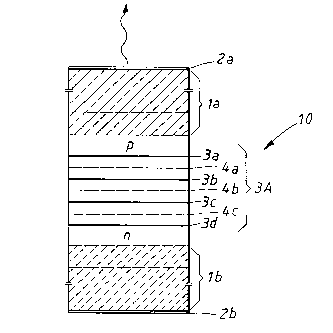
In Fig 2 a device lO is illustrated wherein an optical, verticalcavity is formed by a first and a second dielectric Bragg
reflection device la, lb. The first Bragg reflection device la is
arranged in the upper part of the vertical device and it is
advantageously somewhat transparent. On top of this first
reflecting device an upper contact layer 2a is arranged. In the
shown embodiment this is translucent or transparent. Still further,
in the illustrated emboA;mpnt the lower Bragg reflection device lb
is as reflective as possible and under this a lower contact layer
2b is arranged. Between the two Bragg reflection devices la, lb
four active regions or layers 3a, 3b, 3c, 3d are arranged between
which contact regions or contact layers 4a, 4b, 4c are arranged.
The active regions or the layers 3a, 3b, 3c, 3d are more clearly
illustrated in Fig 2a. In this case the active region is slightly
n-doped (n~). Other alternatives are of course also possible, for
example it could be slightly p-doped (p~), but this constitutes a
technic which as such is known per se. The active regions or the
layers 3a, 3b, 3c, 3d may according to a particular embodiment
form a quantum well structure. The contact regions or the contact
layers 4a, 4b, 4c are more clearly illustrated in Fig lb. The
contact layers 4a, 4b, 4c may according to a particular embodiment
be of the kind of tunnel diodes with thin highly doped layers which
can be seen from the figure. In the illustrated embodiment is shown
how the light is emitted. This can be in form of laser light or of
LED-character, i.e. corresponding to a case as if it is above or
below the threshold current level. In Fig 3 the device according
to Fig 2 is illustrated with a curve illustrating the optical
intensity and it can be seen that each contact layer or contact
region 4a, 4b, 4c is located in a plane corresponding to a minimum r
in optical intensity Iopt whereas each active region 3a, 3b, 3c, 3d
is located in a region corresponding to a maximum in optical
intensity Iopt. An optical standing wave pattern is for example
~ WO9S/07566 PCT/SE94/00803
2 1 6q44;~
introduced through an electrical f~;ng signal I1n, i.e. when I
Px~ the threshold current an optical standing wave pattern is
formed with four (four since according to the embodiment there are
four active regions) intensity peaks. The stAn~;ng wave pattern
declines in the Bragg reflection devices la, lb. The optical losses
are reduced since a maximum only occurs precisely in the active
region. With four active regions 3a, 3b, 3c, 3d four voltage drops
of for example each 1 V is obt~;ne~. (1 V of course merely gives
an example for an illustrative purpose). This would give a total
voltage drop of 4 V. With four active regions 3a, 3b, 3c, 3d the
amplification will be higher without the voltage drop across the
reflectors getting any larger, which voltage drop actually is a
parasitic voltage drop (c.f. Fig l). In the illustrated embodiment
light is emitted upwards (Fig 2). According to alternative
embodiments this could of course be upwards as well as downwards
or in both directions (Fig 3) in which cases the device is adapted
thereto. Through the invention the relative significance of the
reflection losses is reduced at the same time as it gets possible
to reduce the current for a given power, i.e. the impedance is
increased. Then the adaption to cables which normally for example
have an impP~nce of 50 ohm is simplified on even enabled. It has
up to now been very difficult to fabricate transmission cables
which deviate considerably from 50 ohm, c.f. coaxial cables and ~-
strip-cables respectively. Through the invention it will be
possible to vary (increase) the impedance across the active
regions, for example with a factor of 16 of the same time as the
threshold current is lowered with about, for a given power, a
factor 4. (Of course these factors are merely given for
illustrative purposes, corresponding to four active regions.
According to the invention the useful voltage drop, i.e. the
voltage drop across the active regions (corresponding to the power
which is converted to optical power) gets four times greater when
the device comprises four active regions, in a generalized manner
W095/07S66 PCT/SE94/00803
2~ 6~442 ~
n times greater if the device has n active regions, compare the
case as illustrated in Fig 1. Furthermore n (in the shown
embo~;m~nt n=4) gives rise to a higher amplification why a smaller
reflectivity in the reflectors can be accepted since the
requirements thereon decrease, they can be made thinner etc.
In Fig 4 an example of a device according to the invention is
illustrated which has a cylindrical cross section. According to one
embodiment the first Bragg reflection device may have a thickness
of about 2-10 ~m and the second Bragg reflection device may have
a thickness of about 3-10 ~m. With four regions electrically
connected in series forming a complete active region 3A those might
according to the shown embodiment for example have a thickness of
0,75 ~m. The diameter D of the cylindrical device may for example
be about 4 ~m. Of course this merely gives an example and there are
of course a great number of other possibilities.
Examples on materials are GaAlAs (particularly for shorter wave
lengths such as ~=0,8 ~) and InGaAsP for longer wave lengths (for
example ~=1,3-1,6 ~). Of course a number of other materials can
also be used.
The invention is of course not limited to the shown embodiments but
it can be varied in a number of ways within the scope of the
claims. Even if one embodiment with four active layers or regions
has been illustrated, it is of course possible to have fewer as
well as more active regions. Furthermore the active layers and the
electrical contact regions may be of a conventional character, the
reflection devices can take many different forms etc.