Note: Descriptions are shown in the official language in which they were submitted.
216979~
RCA 87,89 1
DATA LINE DRIVERS WITH COLUMN
INITIALIZATION TRANSISTOR
This invention relates generally to drive circuits for display
5 devices and particularly to a system for applying brightness
signals to pixels of a display device, such as a liquid crystal
display (LCD).
Display devices, such as liquid crystal displays, are
composed of a matrix or an array of pixels arranged horizontally
10 in rows and vertically in columns. The video information to be
displayed is applied as brightness (gray scale) signals to data lines
which are individually associated with each column of pixels. The
row of pixels are sequentially scanned and the capacitances of the
pixels within the activated row are charged to the various
15 brightness levels in accordance with the levels of the brightness
signals applied to the individual columns.
In an active matrix display each pixel element includes a
switching device which applies the video signal to the pixel.
Typically, the switching device is a thin film transistor (TFT),
2 0 which receives the brightness information from solid state
circuitry. Because both the TFT.'s and the circuitry are composed
of solid state devices it is preferable to simultaneously fabricate
the TFT's and the drive circuitry utilizing either amorphous silicon
or polysilicon technology.
2 5 Liquid crystal displays are composed of a liquid crystal
material which is sandwiched between two substrates. At least
one, and typically both of the substrates, is transparent to light
and the surfaces of the substrates which are adjacent to the liquid
crystal material support patterns of transparent conductive
30 electrodes arranged in a pattern to form the individual pixel
elements. It may be desirable to fabricate the drive circuitry on
the substrates and around the perimeter of the display together
with the TFT's.
Amorphous silicon has been the preferable technology for
35 fabricating liquid crystal displays because this material can be
fabricated at low temperatures. Low fabrication temperature is
216979~
2 RCA 87,891
important because it permits the use of standard, readily
available and inexpensive substrate materials. However, the use
of amorphous silicon thin film transistors (a-Si TFTs) in integrated
peripheral pixel drivers has been limited because of, low mobility,
5 threshold voltage drift and the availability of only N-MOS
enhancement transistors.
U.S. Patent No. 5,170,155 in the names of Plus et al., entitled
"System for Applying Brightness Signals To A Display Device And
Comparator Therefore", describes a data line or column driver of
10 an LCD. The data line driver of Plus et al., operates as a chopped
ramp amplifier and utilizes TFT's. In the data line driver of Plus
et al., an analog video signal containing picture information and a
reference ramp produced in a reference ramp generator are
applied to a comparator. The comparator controls an output TFT
15 that applies a data ramp voltage to a given data line. During the
interval in which the data ramp voltage ramps, the comparator is
triggered and the output TFT is turned off. Thus, the value of the
data ramp voltage immediately prior to the triggering of the
comparator remains stored in the pixel associated with the data
20 line and forms the pixel signal in the current pixel updating cycle.
In order to prevent the pixel signal stored in the pixel
capacitance in a preceding updating cycle from affecting the pixel
signal stored in the current updating cycle, the stored pixel signal
is discharged prior to the instant that the data ramp voltage
2 5 begins ramping. The comparator is calibrated and,
simultaneously, the output TFT is turned on prior to the ramping
portion of the data ramp voltage and discharges the stored pixel
signal to the level of the data ramp voltage corresponding to a
black level. Because a relatively short time is available for
30 initializing the pixel signal, the output TFT might have to be
driven with a higher gate-to-source voltage than would have been
required for merely applying the data ramp voltage to the data
line. Consequently, the output TFT may be more stressed than
desirable. This results in the conductivity of the output TFT being
3 5 reduced and in the threshold voltage of the TFT being made
susceptible to drift.
216~79~
3 RCA 87,891
A seemingly simple solution, such as increasing the size of
the TFT to increase its conductivity, is undesirable because of the
accompanying increase in gate-source and gate-drain
capacitances. It is desirable to initialize the stored pixel signal
5 without using excessive drive and without increasing the size of
the output TFT.
A data line driver, embodying an aspect of the invention,
applies a video signal to a column electrode of a display device. A
source of the video signal and a source of a data ramp signal are
10 provided. A first transistor is responsive to the video signal for
applying the data ramp signal to the column electrode during a
controllable portion of a period of the data ramp signal that varies
in accordance with the video signal. A column electrode signal is
developed at the column electrode. A second transistor is
15 responsive to an initialization control signal and coupled to the
column electrode for initializing the column electrode signal.
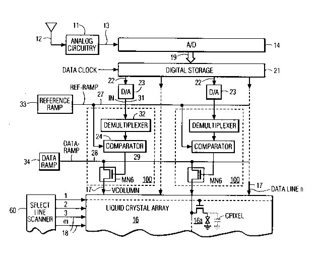
FIGURE 1 illustrates a block diagram of a liquid crystal
display arrangement that includes demultiplexer and data line
drivers, embodying an aspect of the invention;
2 0 FIGURE 2 illustrates the demultiplexer and data line driver
of FIGURE 1 in more detail; and
FIGURES 3a-3h illustrate waveforms useful for explaining
the operation of the circuit of FIGURE 2.
FIGURE 1 illustrates a block diagram of a liquid crystal
2 5 display arrangement that includes demultiplexer and data line
drivers, embodying an aspect of the invention;
FIGURE 2 illustrates the demultiplexer and data line driver
of FIGURE 1 in more detail; and
FIGURES 3a-3h illustrate waveforms useful for explaining
3 0 the operation of the circuit of FIGURE 2.
In FIGURE 1, that includes a multiplexer and data line
drivers 100, embodying an aspect of the invention, an analog
circuitry 11 receives a video signal representative of picture
information to be displayed from, for example, an antenna 12.
35 The analog circuitry 11 provides a video signal on a line 13 as an
input signal to an analog-to^digital converter (A/D) 14.
216979~
.
4 RCA 87,891
The television signal from the analog circuitry 11 is to be
displayed on a liquid crystal array 16 which is composed of a
large number of pixel elements, such as a liquid crystal cell 16a,
arranged horizontally in m = 560 rows and vertically in n = 960
5 columns . Liquid crystal array 16 includes n = 960 columns of data
lines 17, one for each of the vertical columns of liquid crystal cells
16a, and m = 560 select lines 18, one for each of the horizontal
rows of liquid crystal cells 16a.
A/D converter 14 includes an output bus bar 19 to provide
1 0 brightness levels, or gray scale codes, to a memory 21 having 40
groups of output lines 22. Each group of output lines 22 of
memory 21 applies the stored digital information to a
corresponding digital-to-analog (D/A) converter 23. There are 40
D/A converters 23 that correspond to the 40 groups of lines 22,
1 5 respectively. An output signal IN of a given D/A converter 23 is
coupled via a corresponding line 31 to corresponding multiplexer
and data line driver 100 that drives corresponding data line 17.
A select line scanner 60 produces row select signals in lines 18 for
selecting, in a conventional manner, a given row of array 16. The
2 0 voltages developed in 960 data lines 17 are applied during a 32
microsecond line time, to pixels 16a of the selected row.
A given demultiplexer and data line driver 100 uses
chopped ramp amplifiers, not shown in detail in FIGURE 1, with a
low input capacitance that is, for example, smaller than lpf to
2 5 store corresponding signal IN and to transfer stored input signal
IN to corresponding data line 17. Each data line 17 is applied to
560 rows of pixel cells 16a that form a capacitance load of, for
example, 20pf.
FIGURE 2 illustrates in detail a given one of demultiplexer
3 0 and data line drivers 100. FIGURES 3a-3h illustrate waveforms
useful for explaining the operation of the circuit of FIGURE 2.
Similar symbols and numerals in FIGURES 1, 2 and 3a-3h indicate
similar items or functions. All the transistors of demultiplexer
and line driver 100 of FIGURE 2 are TFT's of the N-MOS type.
3 5 Therefore, advantageously, they can be formed together with
array 16 of FIGURE 1 as one integrated circuit.
2169795
S RCA 87,891
Prior to sampling the video signal in signal line 31 of FIGURE
2, a voltage developed at a terminal D of a capacitor C43 is
initialized. To initialize the voltage in capacitor C43, D/A
converter 23 develops a predetermined voltage in line 31 such as
5 the maximum, or full scale voltage of video signal IN. A transistor
MN 1 applies the initializing voltage in line 31 to capacitor C43
when a control pulse PRE-DCTRL of FIGURE 3a is developed at the
gate of transistor MNl. In this way, the voltage in capacitor C43 is
the same prior to each pixel updating cycle. Following pulse PRE-
1 0 DCTRL, signal IN changes to contain video information that is usedfor the current pixel updating cycle.
Demultiplexer transistor MNl of a demultiplexer 32 of
FIGURE 2 samples analog signal IN developed in signal line 31 that
contains video information. The sampled signal is stored in
1 S sampling capacitor C43 of demultiplexer 32. The sampling of a
group of 40 signals IN of FIGURE 1 developed in lines 31 occurs
simultaneously under the control of a corresponding pulse signal
DCTRL(i). As shown in FIGURE 3a, 24 pulse signals DCTRL(i) occur
successively, during an interval following tSa-t20. Each pulse
20 signal DCTRL(i) of FIGURE 2 controls the demultiplexing operation
in a corresponding group of 40 demultiplexers 32. The entire
demultiplexing operation of 960 pixels occurs in interval t5a-t20
of FIGURE 3a.
To provide an efficient time utilization, a two-stage pipeline
2 5 cycle is used. Signals IN are demultiplexed and stored in 960
capacitors C43 of FIGURE 2 during interval t5a-t20, as explained
before. During an interval t3-t4 of FIGURE 3d, prior to the
occurrence of any of pulse PRE-DCTRL and the 24 pulse signals
DCTRL of FIGURE 3a, each capacitors C43 of FIGURE 2 is coupled to
3 0 a capacitor C2 via a transistor MN7 when a pulse signal DXFER of
FIGURE 3d occurs. Thus, a portion of signal IN that is stored in
capacitor C43 is transferred to capacitor C2 of FIGURE 2 and
develops a voltage VC2. During interval tSa-t20, when pulse
signals DCTRL of FIGURE 3a occur, voltage VC2 of FIGURE 2 in
3 S capacitor C2 is applied to array 16 via corresponding data line 17,
216979~ 1
6 RCA 87,891
as explained below. Thus, signals IN are applied to array 16 via
the two-stage pipeline.
A reference ramp generator 33 provides a reference ramp
signal REF-RAMP on an output conductor 27. Conductor 27 is
5 coupled, for example, in common to a terminal E of each capacitor
C2 of FIGURE 2 of each demultiplexer and data line driver 100. A
terminal A of capacitor C2 forms an input terminal of a
comparator 24. A data ramp generator 34 of FIGURE 1 provides a
data ramp voltage DATA-RAMP via an output line 28. In
1 0 demultiplexer and data line driver 100 of FIGURE 2, a transistor
MN6 applies voltage DATA-RAMP to data line 17 to develop a
voltage VCOLUMN. The row to which voltage VCOLUMN is applied
is determined in accordance with row select signals developed in
row select lines 18. A display device using a shift register for
1 5 generating select signals such as developed in lines 18 is
described in, for example, U.S. Patent Nos. 4,766,430 and
4,742,346. Transistor MN6 is a TFT having a gate electrode that is
coupled to an output terminal C of comparator 24 by a conductor
29. An output voltage VC from the comparator 24 controls the
2 0 conduction interval of transistor MN6.
In each pixel updating period, prior to applying voltage VC
of comparator 24 to transistor MN6 to control the conduction
interval of transistor MN6, comparator 24 is automatically
calibrated or adjusted. At time t0 (FIGURE 3b) transistor MN10 is
25 conditioned to conduct by a signal PRE-AUTOZ causing imposition
of a voltage VPRAZ onto the drain electrode of a transistor MN5
and the gate electrode of transistor MN6. This voltage, designated
VC, stored on stray capacitances such as, for example, a source-
gate capacitance C24, shown in broken lines, of transistor MN6
30 causes transistor MN6 to conduct. Transistor MN5 is non-
conductive when transistor MN10 pre-charges capacitance C24.
At a time tl of FIGURE 3b, pulse signal PRE-AUTOZ
terminates and transistor MN10 is turned off. At time tl, a pulse
signal AUTOZERO is applied to a gate electrode of a transistor MN3
3 5 that is coupled between the gate and drain terminals of transistor
MN5 to turn on transistor MN3. Simultaneously, a pulse signal AZ
2169795
7 RCA 87,891
of FIGURE 3g is applied to a gate electrode of a transistor MN2 to
turn on transistor MN2. When transistor MN2 is turned on, a
voltage Va is coupled through transistor MN2 to terminal A of a
coupling capacitor Cl. Transistor MN2 develops a voltage VAA at
5 terminal A at a level of voltage Va for establishing a triggering
level of comparator 24 at terminal A. The triggering level of
comparator 24 is equal to voltage Va. A second terminal B of
capacitor Cl is coupled to transistor MN3 and the gate of
transistor MN5.
1 0 Conductive transistor MN3 equilabrates the charge at
terminal C, between the gate and drain electrodes of transistor
MN5, and develops a gate voltage VG on the gate electrode of
transistor MN5 at terminal B. Initially, voltage VG exceeds a
threshold level VTH of transistor MN5 and causes transistor MN5
1 5 to conduct. The conduction of transistor MN5 causes the voltages
at each of terminals B and C to decrease until each becomes equal
to the threshold level VTH of transistor MN5, during the pulse of
signal AUTOZERO. Gate electrode voltage VG of transistor MN5 at
terminal B is at its threshold level VTH when voltage VAA at
20 terminal A is equal to voltage Va. At time t2 of FIGURES 3c and
3f, transistors MN3 and MN2 of FIGURE 2 are turned off and
comparator 24 is calibrated or adjusted. Therefore, the triggering
level of comparator 24 of FIGURE 2 with respect to input terminal
A is equal to voltage Va.
As explained above, pulse signal DXFER developed,
beginning at time t3, at the gate of transistor MN7 couples
capacitor C43 of demultiplexer 32 to capacitor C2 via terminal A.
Consequently, voltage VC2 that is developed in capacitor C2 is
proportional to the level of sampled signal IN in capacitor C43.
3 0 The magnitude of signal IN is such that voltage VAA developed at
terminal A, during pulse signal DXFER, is smaller than triggering
level Va of comparator 24. Therefore, comparator transistor MN5
remains non-conductive immediately after time t3. ~ voltage
difference between voltage VAA and the triggering level of
3 5 comparator 24 that is equal to voltage Va is determined by the
magnitude of signal IN.
216979~
8 RCA 87, 891
When voltage VAA at terminal A exceeds voltage Va,
transistor MNS becomes conductive. On the other hand, when
voltage VAA at terminal A does not exceed voltage Va, transistor
MNS is nonconductive. The automatic calibration or adjustment of
S comparator 24 compensates for threshold voltage drift, for
example, in transistor MNS.
In carrying out an aspect of the invention, a reset transistor
MN9 is coupled in parallel with transistor MN6, to turn on
transistor MN9 between the column electrode and the data ramp
10 electrode 20. A pulse RESET is applied to the gate electrode of
transistor MN9. The pulse, RESET, has a waveform and timing
similar to that of pulse signal AUTOZERO of FIGURE 3c. When
transistor MN9 of FIGURE 2 is conductive, it applies the current
potential available on conductor 28 to the column bus 17.
15 Transistor MN9 is conditioned to conduct prior to ramping of the
data ramp and thereby to discharge any residual potential on line
17. Advantageously, this prevents previous stored picture
information contained in the capacitance of pixel cell 1 6a from
affecting pixel voltage VCOLUMN at the current update period of
20 FIGURES 3b-3g.
Transistor MN9 establishes voltage VCOLUMN at an inactive
level VIAD of signal DATA-RAMP, prior to time t6. A capacitance
C4 associated with the data line 17 has been partially
charged/discharged toward inactive level VIAD of signal DATA-
2 5 RAMP, during interval tO-tl, immediately after transistor MN10
has been turned on. During pulse signal AUTOZERO, gate voltage
VC of transistor MN6 is reduced to the threshold voltage of
transistor MNS. Therefore, transistor MN6 is substantially turned
off. The charge/discharge of capacitance C4 is performed
3 0 predominantly during interval tl-t2, when transistor MN9 is
turned on. Advantageously, utilizing both transistor MN9 and
transistor MN6, for establishing the initial conditions of voltage
VCOLUMN, reduces a threshold voltage drift of transistor MN6.
The threshold voltage drift of transistor MN6 is reduced because
35 transistor MN6 is driven with a lower gate-source voltage than if
transistor MN9 were absent.
216979~
9 RCA 87,891
Advantageously, transistor MN9 provides an additional
current path between data line 17 and line 28 for pixel voltage
initialization purposes. The additional current path provided by
separate transistor MN9 permits the usage of a transistor MN6
5 that is smaller. Therefore, an undesired increase in the parasitic
gate-source and gate drain capacitances of transistor MN6, that
might have resulted had a larger size transistor MN6 been used, is
avoided.
Transistor MN6 is designed to have similar parameters and
10 stress and, therefore, a similar threshold voltage drift as transistor
MN5. Therefore, advantageously, the threshold voltage drift of
transistor MN6 tracks the threshold voltage drift of transistor
MN5.
In one of two modes of operations that are discussed below,
15 source voltage Vss of transistor MN5 is equal to 0V. Also voltage
VCOLUMN, during interval t2-t4, that is equal to inactive level
VIAD of signal DATA-RAMP, is equal to lV. Drain voltage VC of
transistor MN5 at terminal C, prior to time tS, is equal to threshold
voltage VTH of transistor MN5. Because of the aforementioned
2 0 tracking, variation of threshold voltage VTH of
transistor MN5 maintains the gate-source voltage of transistor
MN6 at a level that is lV less than the threshold voltagè of
transistor MN6. The 1 V difference occurs because there is a
potential difference of one volt between the source electrodes of
2 5 transistors MN5 and MN6.
Advantageously, a pulse voltage C-BOOT of FIGURE 3h is
capacitively coupled via a capacitor C5 of FIGURE 2 to terminal C,
at the gate of transistor MN6. Capacitor C5 and capacitance C24
form a voltage divider. The magnitude of voltage C-BOOT is
30 selected so that gate voltage VC increases with respect to the level
developed, during pulse AUTOZERO, by a predetermined small
amount sufficient to maintain transistor MN6 conductive. As
explained before, transistor MN5 is nonconductive fol!owing time
t3 of FIGURE 3d. Thus, the predetermined increase in voltage VC
3 5 that is in the order of SV is determined by the capacitance voltage
divider that is formed with respect to voltage BOOT-C at terminal
2 1 6 9 7 9 ~
RCA 87,891
C. The increase in voltage VC is independent on threshold voltage
VTH. Therefore, threshold voltage drift of transistor MN5 or MN6
over the operational life, does not affect the increase by voltage C-
BOOT. It follows that, over the operational life when voltage VTH
5 may significantly increase, transistor MN6 is maintained
conductive with small drive prior to time t6 of FIGURE 3f.
Any threshold voltage drift of voltage VTH of transistor
MN5 will cause the same change in voltage VC at terminal C.
Assume that the threshold voltage of transistor MN6 tracks that of
10 transistor MN5. Therefore, voltage C-BOOT need not compensate
for threshold voltage drift of transistor MN6. It follows that
transistor MN6 will be turned on by voltage C-BOOT irrespective
of any threshold voltage drift of transistor MN5 and MN6. Thus,
the threshold voltage variation of transistor MN5 compensates
15 that of transistor MN6.
The capacitance coupling of voltage C-BOOT enables using
gate voltage VC of transistor MN6 at terminal C at a level that is
only slightly greater than the threshold voltage of transistor MN6
such as by 5V over the threshold voltage of transistor MN6.
20 Therefore, transistor MN6 is not significantly stressed. By
avoiding significant drive voltages to the gate electrode of
transistor MN6, advantageously, threshold voltage drift`in
transistor MN6 that may occur over its operational life is
substantially smaller than if transistor MN6 were driven with a
2 5 large drive voltage.
Advantageously, voltage C-BOOT is developed in a ramping
manner during interval t5-t7 of FIGURE 3h. The relatively slow
rise time of voltage C-BOOT helps reduce the stress on transistor
MN6. Having the gate voltage of transistor MN6 increase slowly
30 allows the source of transistor MN6 to charge such that the gate-
source potential difference remains smaller for larger periods.
Interval t5-t7 has a length of 4~1sec. By maintaining the length of
interval t5-t7 longer than 2,usec, or approximately 20G~o of the
length of interval t6-t8 of signal DATA-RAMP of FIGURE 2f, the
3 5 voltage difference between the gate and the source voltage in
21 6979~
1 1 RCA 87,891
transistor MN6 is, advantageously, reduced for a significantly
large period. Therefore, stress is reduced in TFT MN6.
At time t4 of FIGURE 3e, reference ramp signal REF-RAMP
begins up-ramping. Signal REF-RAMP is coupled to terminal E of
5 capacitor C2 of FIGURE 2 that is remote from input terminal A of
comparator 24. As a result, voltage VAA at input terminal A of
comparator 24 is equal to a sum voltage of ramping signal REF-
RAMP and voltage VC2 developed in capacitor C2.
Advantageously, during interval tl-t2 of FIGURE 3c, when
1 0 the automatic triggering voltage adjustment or calibration of
comparator 24 occurs, transistor MN2 couples voltage Va to
capacitor C2 via terminal A, that is remote from reference ramp
generator 33. Similarly, during interval t3-t4, when the charge is
transferred to capacitor C2, transistor MN7 is coupled to capacitor
1 5 C2 via terminal A that is remote from ramp generator 33. Thus,
terminal E of capacitor C2, advantageously, need not be decoupled
from conductor 27 of reference ramp generator 33. Because
terminal E need not be decoupled from reference ramp generator
33, signal REF-RAMP is coupled to terminal A of comparator 24
2 0 without interposing any TFT switch between conductor 27 of
reference ramp generator 33 and terminal A. A TFT in the signal
path might have suffered from threshold voltage drift.
Advantageously, conductor 27 may be common to several units of
multiplexer and data drivers 100.
2 5 Following time t6, data ramp voltage DATA-RAMP coupled
to the drain electrode of transistor MN6 begins upramping. With
feedback coupling to terminal C from the stray gate-source and
gate driven capacitance of transistor MN6, the voltage at terminal
C will be sufficient to condition transistor MN6 to conduct for all
3 0 values of the data ramp signal DATA-RAMP. Following time t4,
and as long as ramping voltage VAA at terminal A has not
reached the triggering level that is equal to voltage Va of
comparator 24, transistor MN5 remains non-conductive and
transistor MN6 remains conductive. As long as transistor MN6 is
3 5 conductive, upramping voltage DATA-RAMP is coupled through
transistor MN6 to column data line 17 for increasing the potential
21 6979~ 1
12 RCA 87,89 1
VCOLUMN of data line 17 and, therefore, the potential applied to
pixel capacitance CPIXEL of the selected row. The capacitive
feedback of ramp voltage VCOLUMN via, for example, capacitance
24, sustains transistor MN6 in conduction, as long as transistor
5 MN5 exhibits a high impedance at terminal C, as indicated before.
At some time during the upramping portion 500 of signal
REF-RAMP of FIGURE 3e, the sum voltage VAA at terminal A will
exceed the triggering level Va of comparator 24, and transistor
MN5 will become conductive. The instant that transistor MN5
10 becomes conductive is determined by the magnitude of signal IN.
When transistor MN5 becomes conductive, gate voltage VC
of transistor MN6 decreases and causes transistor MN6 to turn off.
As a result, the last value of voltage DATA-RAMP that occurs prior
to the turn-off of transistor MN6 is held unchanged or stored in
15 pixel capacitance CPIXEL until the next updating cycle. In this
way, the current updating cycle is completed.
In order to prevent polarization of liquid crystal array 16 of
FIGURE 1, a so-called backplane or common plane of the array, not
shown, is maintained at a constant voltage VBACKPLANE.
2 0 Multiplexer and data line driver 100 produces, in one updating
cycle, voltage VCOLUMN that is at one polarity with respect to
voltage VBACKPLANE and at the opposite polarity and the same
magnitude, in an alternate updating cycle. To attain the alternate
polarities, voltage DATA-RAMP is generated in the range of 1 V-
2 5 8.8V in one updating cycle and in the range of 9V-16.8V in the
alternate update cycle. Whereas, voltage VBACKPLANE is
established at an intermediate level between the two ranges.
Because of the need to generate voltage DATA-RAMP in two
different voltage ranges, signals or voltages AUTOZERO, PRE-
3 0 AUTOZ, Vss and RESET have two different peak levels that changein alternate updating cycles in accordance with the established
range of voltage DATA-RAMP.