Note: Descriptions are shown in the official language in which they were submitted.
CA 02169999 1999-10-08
WIDE-BAND SIGNAL ENCODER
The present invention relates to a wide-band signal
encoder for high quality encoding of wide-band signals, such
as an audio signal, with low bit rates, particularly about 64
kb/s.
As a prior art system for encoding a wide-band signal,
such as an audio signal, with a low bit rate, typically about
128 kb/s per channel, a well-known audio encoding system is
disclosed in "Transform Coding of Audio Signals Using
Perceptual Noise Criteria", IEEE Journal on Selected Areas in
Communications, ~iTol. 6, No. 2, pp. 314-323, February 1988, by
Johnston.
In that method, on the transmitting side an input
signal is converted into frequency components through FFT for
each block (for instance 2,048 samples), the FFT components
thus obtained are divided into 25 critical bands, an
acoustical masking threshold is then calculated for each
masking threshold, and a quantization bit number is assigned
to each critical band on the basis of the masking threshold.
In addition, the FFT components are staler quantized according
to the quantization bit numbers. The staler quantization
information, bit assignment information and quantization step
size information are transmitted in combination for each block
to the receiving side. The receiving side is not described.
In the above prior art method, (1) the quantization
efficiency is not very high because of the sealer quantization
used for the quantization of the FFT components, and (2) no
inter-block bit assignment is provided, although bit
assignment is made for intro-block FFT components so that
sufficient gain due to the bit assignment cannot be obtained
- 1 -
CA 02169999 1999-10-08
for transient signals. Therefore, bit rate reduction down to
about 64 kb/s results in quantization efficiency reduction
which extremely deteriorates the sound quality.
According to a first aspect of the present invention,
a block length is determined by obtaining a sample quantity
from the input signal, and transformation of the input signal
into frequency components is executed for each block length.
Appropriate transforms are MCDT (Modified Discrete Cosine
Transform), DCT (Discrete Cosine Transform) or a transform
with a band division band-pass filter bank. For details of
the MDCT, reference is made to Princen et al., "Analvsis-
Synthesis Filter Bank Design Based on Time Domain Aliasing
Cancellation", IEEE Transactions on Acoustics, Speech, and
Signal Processing, Vol. ASSP-34, No. 5, pp. 1153-1161, October
1986. A masking threshold is obtained from the output of a
transform circuit or from the input signal on the basis of an
acoustical masking characteristic, and an inter-block
quantization bit number and/or assignments of an intra-bit
quantization bit number corresponding to a transform circuit
output vector axe determined on the basis of the masking
threshold. The transform output signal is vector quantized
using a codebook, of a bit number corresponding to the bit
assignment, and an optimum codevector is selected from the
codebook.
According to a second aspect of the present invention,
a prediction error signal is obtained through prediction of
a transform signal for the present block from a quantized
output signal for a past block. The masking threshold is
obtained from the transform output, the input signal or the
prediction error signal on the basis of an acoustical masking
characteristic. Assignments of the inter-block quantization
- 2 -
CA 02169999 1999-10-08
bit number and/or the intra-block quantization bit number
corresponding to a transform output vector are determined on
the basis of the obtained masking threshold. The transform
output signal is vector quantized using a codebook for the bit
number corresponding to the bit assignment, and an optimum
codevector is selected from the codebook.
According to a third aspect of the present invention,
a prediction error signal is obtained by predicting the
transform output signal for the present block from a quantized
output signal for a past block and a prediction signal for a
past block. A. masking threshold is obtained from the
transform output, the input signal or the prediction error
signal on the basis of an acoustical masking characteristic.
Assignment of the intra-block quantization bit number is
determined on the basis of the masking value. The transform
output signal is vector quantized using a codebook for a bit
number corresponding to the bit assignment.
A fourth aspect of the present invention was a fixed
block for the transform, and the total bit number of each is
also fixed. This aspect eliminates block length determination
and the inter-block bit assignment according to the second
aspect of the invention.
A fifth aspect of the present invention was a fixed
block for the transform, and the total bit number of each is
also fixed. This aspect eliminates block length determination
and the inter-block bit assignment according to the third
aspect of the invention.
In a sixth aspect of the present invention, the
transform output or the prediction error signal according to
one of the first to fifth aspects of the present invention is
- 3 -
CA 02169999 1999-10-08
vector quantized while weighting the signal by using the
masking threshold.
In a seventh aspect of the present invention, the
transform output or the prediction error signal according to
one of the first to fifth aspects of the present invention is
vector quantized after processing the signal on the basis of
a psychoacoustical property.
In an eighth aspect of the present invention, a low
degree spectrum coefficient representing a frequency envelope
of the transform output signal from the transform circuit or
the prediction error signal according to one of the first to
fifth aspects of the present invention is obtained, and the
transform output or the prediction error signal is quantized
by using the frequency envelope and the output of the bit
assignment circuit.
Further aspects of the present invention there is
provided a wide-band signal encoder comprising: a block length
judging circuit for determining a block length based on a
feature quantity obtained from an input signal; a transform
circuit for executing transform of the input signal into
frequency components through division of the input signal into
a plurality of blocks having a predetermined time length; a
masking threshold calculating circuit for obtaining a masking
threshold from the output of the transform circuit and the
input signal on the basis of an acoustical masking
characteristic; a bit assignment circuit for determining an
inter-block quantization bit number and/or an intra-block
quantization bit number in a predetermined section not shorter
than the block length on the basis of the obtained masking
threshold; and a vector quantization circuit for quantizing
- 4 -
CA 02169999 1999-10-08
the output signal of the transform circuit according to the
output of the bi,t assignment circuit.
The present invention will now be described, by way
of example, with reference to the accompanying drawings,
wherein:
Figure 1 is a block diagram showing an embodiment of
a wide-band signal encoder according to a first aspect of the
present invention;
Figure 2 is a block diagram showing an embodiment of
the wide-band signal encoder according to a second aspect of
the present invention;
Figure 3 is a block diagram showing a structure
according to a third aspect of the present invention;
Figure ~ is a block diagram showing a structure
according to a fourth aspect of the present invention;
Figure 5 is a block diagram showing a structure
according to a fifth aspect of the present invention;
Figure 6. is a block diagram showing a structure
according to a sixth aspect of the present invention;
Figure 7 is a block diagram showing an example of a
weighting vector quantization circuit (700);
Figure 8 is a block diagram showing a structure
according to a seventh aspect of the present invention;
Figure 9 is a block diagram showing a structure
according to an eighth aspect of the present invention; and
Figure 10 is a block diagram showing an arrangement
in which prediction error signal is quantized.
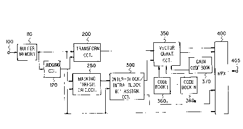
Figure 1 shows an embodiment of a wide-band signal
encoder according to a first aspect of the present invention.
Referring to Figure l, in the transmitting side of a system,
a wide-band signal is inputted from an input terminal 100, and
- 5 -
CA 02169999 1999-10-08
one block of signal having a maximum block length (for
instance 1,024 samples) is stored in a buffer memory 110. A
block length judging circuit 120 was a predetermined feature
quantity to determine whether the intra-block signal is
transient or steady-state. In the circuit 120 a plurality of
different block lengths are available. For the sake of
brevity, it is assumed that two different block lengths, for
instance a 1,024-sample block and a 256-sample block, are
available. The feature quantity may be intra-block signal
power-changes with time, predicted gain, etc.
A transform circuit 200 receives a signal from the
buffer memory 110 and block length data (representing either
a 1,024- or 256-sample block, for instance) from the block
length judging circuit 120, chooses a signal corresponding to
the pertinent block length, multiplies the chosen signal by
a window, and executes an 1~CT transformation on the
multiplied signal. A masking threshold calculating circuit
250 receives the output from the block length judging circuit
120 and the output signal from the buffer memory 110 and
calculates a masking threshold value corresponding to the
signal for the block length. The masking threshold
calculation may be made as follows. FFT is performed on the
input signal x (n) for the block length to obtain spectrum X (k)
(k being 0 to N-l.) and also to obtain power spectrum ~X(k)~z,
which is analyzed by using a critical band-pass filter or an
acoustical model to calculate power or RMS for each critical
band. The power calculation is as follows:
- ~k.=blibhi ~ X (k) ~ 2 (1=1 t0 R) . . . . . . . . (1)
- 6 -
CA 02169999 1999-10-08
where bl; and bhl are the lower and upper limit frequencies in
the i-th critical band. R represents the number of the
critical bands included in the speech signal band~
Then, a variance function is convoluted to the
critical band spectrum as:
~a=1 Bi sPrd ( j . i ) . . . . . . .
~ (2)
where sprd (j,i;) is the variance function. For specific
values of the function, reference is made to Johnston cited
above. b~x is the number of critical bands contained up to
angular frequency n.
Then, masking threshold spectrum T'i is calculated as
T'i - C:~ Tl . . . . . . . . ( 3 )
where
Ti _ 10-co~~io> . . . . . . . . (4)
Oi - a (14.5 + i) + 1 (1 - a) 5 .5 . ~ ~ , . " . (5)
a - miry [ (NG/R) , 1. 0] . . . . . . . . (6)
Here, NG is the predictability, and for its
calculation methad reference is made to Johnston cited above.
When the absolute threshold is taken into consideration, the
masking threshold spectrum T"i is expressed as
T~i - max [Ti, absth~] , , , , , , ,
CA 02169999 1999-10-08
where absthl is the absolute threshold in the critical band i,
and is taught in Johnston cited above.
The masking threshold spectrum data is outputted to
an inter-block/intra-block bit assignment circuit 300. The
inter-block/intra-block bit assignment circuit 300 receives
the masking threshold for each critical band and the output
of the block length judging circuit 120 and, when the block
length is 1,024 samples, executes only the intra-block bit
assignment. When the block length is 256 samples, the circuit
300 calculates the bit number Bi (i being 1 to 4) of each of
four successive blocks (i.e., a total of 1,024 samples), and
then executes the intra-block bit assignment with respect to
each of the four blocks. In the intra-block bit assignment
circuit 300, bit: assignment is executed for each critical
band.
The intra-block bit assignment is made as follows.
Signal-to-masking threshold ratio SMR~i (j being 1 to B~, i
being 1 to 4, and B~ being the number of critical bands), is
obtained as
Ri = R+1/21og2 (II~~OM-iSMR~i] 1/M/ ~~l-iL~,aOM-ls~jl~ 1/MxI.
........(8)
where Ri is the :number of assignment bits to the i-th sub-
frame, R is the average bit number of quantization, M is the
number of critical bands, and L is the number of blocks.
Another method of bit assignment is as follows:
Rl = R+1/21og2 L~i=oM iSMR~l] 1/M/ ~ni~ly~~=oM iSMR~i] 1/M
........(9)
_ g _
CA 02169999 1999-10-08
The bit assignment of critical band k in i-th block is
Rki = R+1~21og2 LSMRki] ~ [IIisiLSMRki] 1/L . . . . . . . . (lU)
or
Rki = R+1~21og2 LSMRki] ~ LIIk~IMSMRki] 1/L . . . . . . . . (11)
where Rki is k-th band in i-th sub-frame (i being 1 to L, k
being 1 to Bm"~) , and
Ski = pki~Tki . . . . . . . . ( 1 Z )
where Pki is the input signal power in each divided band of
i-th block, and Tki is the masking threshold for each critical
band of i-th block.
In order that the bit number in the whole block is a
predetermined value as given below, bit number adjustment is
executed to confine the sub-frame assignment bit number
between a lower limit bit number and an upper limit bit
number.
~~=i LRi = Rr . . . . . . . . ( 13 )
Ran < R~ < R,~x . . . . . . . . ( 14 )
where R~ is the number of bits assigned to j-th block, RT is
the total bit number in a plurality of blocks (i.e., 4
blocks), Rte" is the lower limit bit number in the block, and
_ g _
CA 02169999 1999-10-08
1~"x is the upper limit bit number in the block. L is the
number of blocks (i.e., 4 in this example). The bit
assignment data obtained as a result of the above processing,
is outputted to a vector quantization circuit 350 and also to
a multiplexer 400.
The vector quantization circuit 350 has a plurality
of excitation c:odebooks 3601 to 360n, each different in
assignment bit number from a minimum bit number to a maximum
bit number. Th.e circuit 350 receives the assignment bit
number data for each intra-block critical band, and selects
a codebook according to the bit number. Then it selects an
excitation codevector for each critical band to minimize the
quantization signal Em according to the following:
Em = ~n=oNk-1 (Xk (n) - Y~ ' C,~ (n) ] Z . . . . . . . . ( 15 )
where Xk(n) is an MDCT coefficient contained in the k-th
critical band, Nk is the number of MDCT coefficients contained
in the k-th critical band, and Y,~ is the optimum gain for
codevector C,~(n) (m being 0 to 28k-1, Bk being the bit number
of excitation codebook for the k-th critical band). An index
representing the selected excitation codevector is outputted
to the multiplexer 400.
The excitation codebooks may be organized from
Gaussian random numbers or by preliminary study. A method of
codebook organization by study is taught in, for instance,
Linde et al., °An Algorithm for Vector Quantizer Design~~, IEEE
Transactions on Communications, Vol. COM-28, No. 1, pp. 84-95,
January 1980.
- 10 -
r
CA 02169999 1999-10-08
Using the selected excitation codevector C,~(n) and a
gain codebook 370, a gain codevector is retrieved to minimize
Em according to the following equation:
Em - ~n=oNk-1 LXk (n) - gx~ ' Cxm (n) 1 Z . . . . . . .
. (16)
where g~ is the m-th gain codevector in the k-th critical
band. An index of the selected gain codevector is outputted
to the multiplexer 400.
At output terminal 405 the multiplexer 400 outputs in
combination the output of the block length judging circuit
120, the output of the intro-block/inter-block bit assignment
circuit 300, and indexes of the excitation codevector and the
gain codevector .from the vector quantization circuit 350.
Figure 2 is a block diagram showing an embodiment of
a wide-band signal encoder according to a second aspect of the
present invention. In Figure 2, constituent elements
designated by reference numerals like those in Figure 1
operate likewise,, and are not described here.
A delay circuit 510 causes delay of the output Z'(k)
of the vector quantization circuit 350 for a past block to an
extent corresponding to a predetermined number of blocks. The
number of blocks may be any number, but it is assumed to be
one for the sake of the brevity of the description.
A prediction circuit 500 predicts the transform
component Y (k) by using the output Z (k) -1 of the delay circuit
as
Y (k) - A (k) ' Z (k) w (k=1 to L/2 ) . . . . , , . . (17 )
- 11 -
CA 02169999 1999-10-08
where A(k) is a prediction coefficient, and L is the block
length. A(k) is determined beforehand with respect to a
training signal. Y(k) is outputted to a subtractor 410.
The subtractor 410 calculates the prediction signal
Y(k) from the output X(k) of the transform circuit 200 as
follows and outputs a prediction error signal Z(k).
Z (k) - X (k) - Y (k) (k=1 to L/2) . . . . . . . , (18)
Figure 3 is a block diagram showing a structure
according to a third aspect of the present invention. In
Figure 3, constituent elements designated by reference
numerals like those in Figures 1 and 2 operate likewise, and
are not described here.
A summation circuit 420 adds the output Y(k) of the
prediction circuit 530 and the output Z~(k) of the vector
quantization circuit 350 and outputs the sum S (k) to the delay
circuit 510.
The prediction circuit 530 executes the prediction by
using the output of the delay circuit 510 as follows:
Y (k) - B (k) ~ S (k) -1 (k=1 to L/2) . . . . . . . . (19)
where B(k) is a prediction coefficient, and L is the block
length. B(k) is determined beforehand with respect to a
training signal. Y(k) is outputted to the subtractor 410.
Figure 4 is a block diagram showing a structure
according to a fourth aspect of the present invention. In
Figure 4, constituent elements designated by reference
numerals like those in Figure 2 operate likewise, and are not
described here. According to the fourth aspect of the present
- 12 -
CA 02169999 1999-10-08
invention, the block length for transform is fixed, and also
the total bit number of each block is fixed. This aspect of
the present invention is therefore different from the second
aspect of the present invention (Figure 2) in that the block
length judging circuit 120 is unnecessary and that only intra-
block bit assignment is made.
An intra-block bit assignment circuit 600 executes bit
assignment with respect to a transform component in each
intra-block critical band on the basis of the equations (10)
to (14) .
Figure 5 is a block diagram showing a structure
according to a fifth aspect of the present invention. In
Figure 5, constituent elements designated by reference
numerals like those in Figures 3 and 4 operate likewise, and
are not described here. According to the fifth aspect of the
present inventian, like the third aspect of the present
invention, the block length for transform is fixed, and also
the total bit number of each block is fixed. The differences
from the third aspect of the present invention are that the
block length judging circuit 120 is unnecessary and that only
intra-block bit assignment is made.
Figure 6 is a block diagram showing a structure
according to a sixth aspect of the present invention. This
structure is different from the Figure 1 structure according
to the first aspect of the present invention in that a
weighting vector quantization circuit 700 and codebooks 6101
to 610N are included. The structure of the weighting vector
quantization circuit 700 will now be described.
Figure 7 is a block diagram showing an example of the
weighting vector quantization circuit 700. A weighting
coefficient calculation circuit 710 receives masking threshold
- 13 -
CA 02169999 1999-10-08
data Tki from the masking threshold calculating circuit 250
and calculates and outputs a weighting coefficient for the
vector quantization (tlki). For the calculation, reference is
made to the following:
~ki - l~Tki (k=1 t0 B~)
where B~ is the number of critical bands contained in one
block.
A weighting vector quantization circuit 720 receives
data of number R~;i of bits assigned to the k-th critical band
in the i-th block, selects one of codebooks 6101 to 610N
according to the bit number, and executes weighting vector
quantization of transform coefficient X(n) as:
LrazpNk 1 ~Xk (n) - Ykm ~ Ckm (n) ~ 2 ~ ~ki
........ (20)
Also, the circuit 720 executes gain quantization by
using a gain codebook 370.
The weighting vector quantization circuit 700 may be
added to the second to fifth aspects of the present invention
by replacing the vector quantization circuit 350 with it.
Figure 8 is a block diagram showing a structure
according to a seventh aspect of the present invention. In
the case of this structure, a process based on a
psychoacoustical property is introduced to the first aspect
of the present invention shown in Figure 1.
A psychoacoustical property process circuit 820
executes a transform based on the psychoacoustical property
- 14 -
CA 02169999 1999-10-08
with respect to the output X(n) of the transform circuit 200
as:
Q (n) - F [X (n) ] . . . . . . . . (21)
where F[X(n)] represents the transform based on the
psychoacoustical property. Specifically, such transforms as
Burke's transform, masking process, loudness transform, etc.
are applicable. For details of these transforms, reference
is made to Wang et al., "An Objective Measure for Predicting
Subjective Quality of Speech Coders", IEEE Journal on Selected
Areas in Communications, Vol. SAC-10, No. 5, pp. 819-829, June
1992, and these 'transforms are not described herein.
A vector quantization circuit 800 switches codebooks
3601 to 360N according to the assignment bit number data
received for each critical band in each block from the inter
block/intra-block bit assignment circuit 300, and vector
quantizes Q(n) as:
Em - ~n~oNk-1 IQx (n) - Y,~' F LC,~, (n) ] ] Z . . . . . . . . (22 )
Here, use is made of a method of codevector retrieval while
executing a transform based on the psychoacoustical property
with respect to codevector C,~(n) received from the codebook.
In the case where the codevector obtained as a result of a
transform on the basis of the psychoacoustical property, i . a . ,
codevector F [C,~ (n) ] , is stored in advance in the codebook,
the vector quantization given as:
Em - L,a=ONk 1 [ Qk ( n ) - Yxm ' Pxm ( n ) 1 2 . . . . . . . . ( 2 3 )
- 15 -
CA 02169999 1999-10-08
may be executed. Here
P,~ (n) - F [C,~ (n) ] . . . . . . . . (24)
After the codevector retrieval, gain y~ may be quantized
using the gain cadevector obtained from the gain codebook 370.
The process based on the psychoacoustical property may
be introduced to the second to fifth aspects of the present
invention by replacing the vector quantization circuit 350
with the vector quantization circuit 800 and adding a
psychoacoustical property process circuit 820 to the input
section of the circuit 800.
Figure 9 is a block diagram showing a structure
according to the eighth aspect of the present invention. In
Figure 9, constituent elements designated by reference
numerals like those in Figure 1 operate likewise, and are not
described here.
A spectrum coefficient calculating circuit 900
calculates a low degree spectrum coefficient, which
approximates the frequency envelope of I~CT coefficient X(n)
(n being 1 to L) from the output of the transform circuit 200.
For the spectrum coefficient, LPC (Linear Prediction
Coefficient), cepstrum, mercepstrum, etc. are well known in
the art. In the present invention LPC is used. X2(n) (n-1 to
L) is subjected to inverse I~CT or inverse FFT to obtain self-
correlation R(n).. The self-correlation R(n) is taken up to
a predetermined degree z, and LPC coefficient a (i) (i being
1 to z ) is calculated from R (n) .
A quantizing circuit 910 quantizes the LPC
coefficient. The circuit 910 preliminary converts the LPC
coefficient into an LSP (Line Spectrum Pair) coefficient
- 16 -
CA 02169999 1999-10-08
having a higher quantization efficiency for quantization with
a predetermined number of bits . For the conversion of the LPC
coefficient to the LSP coefficient, reference is made to
Sugamura et al., "Quantizer Design in LSP Speech Analysis-
Synthesis", IEEE Journal on Selected Areas in Communications,
Vol. 6, No. 2, pp. 432-440, February 1988. The quantization
may be staler quantization or vector quantization. The index
of the quantized LSP is outputted to the multiplexer 400. In
addition, the quantized LSP is decoded and then inversely
converted to LPCa'(i) (i being 1 to z). LPCa'(i) thus
obtained is then subjected to 1~CT or FFT for calculating a
frequency spectrum H(n) (n being 1 to L/2) which is outputted
to a vector quantization circuit 930.
The vector quantization circuit 930 normalizes the
output X (n) of the transform circuit 200 by using spectrum
H(n) according to the following:
X' (n) _ X (n) /H (n) (n=1 to L/2) . . . . . . . . (25)
Then it executes vector quantization of X'(n) by selecting a
codevector which minimizes Em, according to the following:
Em - L.,n=or"'-1 IXrk (n) - C,~ (n) ] Z . . . . . . . . (26)
The spectrum H(n) used has an effect of normalizing
the gain, so that no gain codebook is required.
The Figure 9 structure may also use the block length
judging circuit :120 for switching the block length and the
inter-block/intra-block bit assignment circuit 300.
Figure 10 is a block diagram showing an arrangement
in which prediction error signal is quantized. In Figure 10,
- 17 -
CA 02169999 1999-10-08
constituent elements designated by reference numerals like
those in Figures 1 and 9 operate likewise, and are not
described here.
In this case, a vector quantization circuit 950
normalizes the prediction error signal Z(n) from the output
of the subtractor 410, according to the following:
Z' (n) _ Z (n) / H (n) (n-1 to L/2 ) . . . . . . . . (27 )
Then, vector quantization of Z'(n) is made by selecting a
codevector which minimizes Em, according to the following:
Em - (rn=ONk 1 LZ'k (n) - C,~ (n) ] 2 . . . . . . . . (28)
The Figure 10 structure may also use the block length
judging circuit 120 for switching the block lengths and the
inter-block/intra-block bit assignment circuit 300. As a
further alternative, the prediction error signal Zn may be
calculated by using the Figure 3 method.
According to the present invention as described above,
as a method of bit assignment determination it is possible to
design bit assignment codebooks corresponding in number to a
predetermined number of patterns (for instance 28, B being a
bit number indicative of a pattern) by clustering SMR and
tabulating each cluster of SMR and each assignment bit number,
and permit these codebooks to be used in the bit assignment
circuit for the bit assignment calculation. With this
arrangement, the bit assignment information to be transmitted
may only be B bits per block, and thus it is possible to
reduce the bit assignment information to be transmitted.
- 18 -
CA 02169999 1999-10-08
A further alternative is that the vector quantization
circuit 350 may vector quantize the transform coefficient or
the prediction error signal by using a different extent
measure. A still further alternative is that the weighting
vector quantization using the masking threshold according to
the sixth aspect of the present invention may use a different
weighting extent measure.
A further alternative is that the intra-block bit
assigxunent according to the first to eighth aspects of the
present invention may be performed for each predetermined
section instead of each critical band.
A yet further alternative is that the bit assignment
for each inter-block and/or intra-block critical band
according to the first to third, sixth and seventh aspects of
the present invention may use an equation other than equation
(4), for instance:
Rk~ = R+1,~21og2 [II~IQkSMR~~] / ~n~~lL~ukSMRxm~] 1/Qy
........ (29)
where Qk is the number of critical bands contained in k-th
division band.
As an alternative to the bit assignment method in the
bit assignment circuit, it is possible that after making a
preliminary bit assignment on the basis of the equations (8)
to (12), the quantization using a codebook corresponding to
the actually assigned bit number is executed for measuring
quantized noise and adjusting the bit assignment such as to
maximize
3 0 MNR~ - III,i~yM-lSMRi~ ] 1/M/~~~2 . . . . . . . . ( 3 0 )
- 19 -
CA 02169999 1999-10-08
where 6n~z is quantized noise measured in the j-th sub-frame.
The above masking threshold spectrum calculation
method may be replaced with a different method well-known in
the art.
The masking threshold calculating circuit 250 may use
a band division filter group in lieu of the Fourier Transform
in order to reduce the amount of operations. For the band
division, QMFs (Quadrature Mirror Filters) are used. The QMF
is detailed in P. Vaidyanathan, "Multirate Digital Filters,
Filter Banks, Polyphase Networks, and Applications: A
Tutorial", Proceedings of the IEEE, Vol. 78, No. 1, pp. 56-93,
January 1990.
As has been described in the foregoing, according to
the present invention the transform coefficient or the
prediction error signal obtained by predicting the transforan
coefficient is vector quantized after making the inter-block
and/or intra-block bit number assignment. It is thus possible
to obtain satisfactory coding of a wide-band signal even with
a lower bit rake than in the prior art. In addition,
according to the present invention reduction of auxiliary
information is possible by expressing the transform
coefficient or prediction error signal frequency envelope with
a low degree spectrum coefficient, thus permitting realization
of lower bit rates than in the prior art.
Various additional modifications and embodiments of
the present invention apparent to those skilled in the art do
not depart from the scope of the invention. The matter sat
forth in the foregoing description and accompanying drawings
is offered for illustrative purposes only. It is understood
that the foregoing description be regarded as illustrative
rather than limiting.
- 20 -