Note: Descriptions are shown in the official language in which they were submitted.
WO 95/06307 PCT/US94/09217
2I 702~;~
"ELECTROPHORETIC DISPLAY HAVING REDUCED WRITING TIME"
s
BACKGROUND ART
Electrophoretic displays (EPIDS) are now well known. A variety
of display types and features are taught in several patents issued in the names
of the inventors herein, Frank J. DiSanto and Denis A. Krusos and assigned to
the ~ignee herein, Copytele, Inc. of ~lln~ington Station, New York. For
example, U.S. Patent Nos. 4,655,897 and 4,732,830, each entitled
ELECTROPHORETIC DISPI~Y PANELS AND ASSOCIATED METHODS
describe the basic operation and construction of an electrophoretic display.
U.S. Patent No. 4,742,345, entitled ELECIROPHORETIC DISPI~Y PANELS
AND METHODS THEREFOR, describes a display having i~ roved ~lignment
and contrast. Many other patents regarding such displays are also assigned to
Copytele, Inc.
The display panels shown in the above-mentioned patents operate
upon the same basic principle, viz., if a suspension of electrically charged
pigment particles in a dielectric fluid is subjected to an applied electrostaticfield, the pigment particles will migrate through the fluid in response to the
electrostatic field. Given a substantially homogeneous suspension of particles
having a pigment color different from that of the dielectric fluid, if the applied
electrostatic field is localized it will cause a visually observable localized
pigment particle migration. The localized pigment particle migration results
either in a localized area of concentration or rarefaction of particles depending
upon the polarity and direction of the electrostatic field and the charge on thepigment particles.
WO9S/06307 ~,6~ PCT/U594/09217
The electrophoretic display apparatus taught in the foregoing
U.S. Patents are "triode-type" displays having a plurality of independent,
parallel, cathode row conductor elements or "lines" deposited in the horizontal
on one surface of a glass viewing screen. A layer of ins~ ting photoresist
material deposited over the cathode elements and photoetched down to the
cathode elements to yield a plurality of in~ tQr strips positioned at right
angles to the cathode elements, forms the substrate for a plurality of
independent, parallel column or grid conductor elements or "lines" running in
the vertical direction. A glass cap member forms a fluid-tight seal with the
viewing window along the cap's peripheral edge for cont~ining the fluid
suspension and also acts as a substrate for an anode plate deposited on the
interior flat surface of the cap. When the cap is in place, the anode surface isin spaced parallel relation to both the cathode elements and the grid elements.
Given a specific particulate suspension, the sign of the electrostatic charge
which will attract and repel the pigment particles will be known. The cathode
element voltage, the anode voltage, and the grid element voltage can then be
ascertained such that when a particular voltage is applied to the cathode and
another voltage is applied to the grid, the area proxim~te their intersection will
assume a net charge sufficient to attract or repel pigment particles in
suspension in the dielectric fluid. Since numerous cathode and grid lines are
employed, there are numerous discrete intersection points which can be
controlled by varying the voltage on the cathode and grid elements to cause
localized visible regions of pigment concentration and rarefaction. Essentially
then, the operating voltages on both cathode and grid must be able to ~c~llme
at least two states corresponding to a logical one and a logical zero. Logical
one for the cathode may either correspond to attraction or repulsion of
pigment. Typically, the cathode and grid voltages are selected such that only c
~ WO 95/06307 2 ~1 7 0 2 6 3 PCT/US94/09217
when both are a logical one at a particular intersection point, will a sufficient
electrostatic field be present at the intersection relative to the anode to cause
the writing of a visual bit of information on the display through migration of
pigment particles. The bit may be erased, e.g., upon a reversal of polarity and
a logical zero-zero state occurring at the intersection coordinated with an erase
voltage gradient between anode and cathodé. In this manner, .ligiti7lod data
can be displayed on the electrophoretic display.
Besides the triode-type display, the applicant's herein have
proposed a variety of EPID structures for utilizing the electrophoretic effect.
For example, an alternative EPID construction is described in Application No.
07/345,825, now U.S. Patent No. 5,053,763, entitled DUAL ANODE FI~T
PANEL ELECTROPHORET~C DISPI~Y APPAR~TUS, which relates to an
electrophoretic display in which the cathode/grid matrix as found in triode-typedisplays is overlayed by a plurality of independent, separately addressable
"local" anode lines. The local anode lines are deposited upon and aligned with
the grid lines and are insulated therefrom by interstitial lines of photoresist.The local anode lines are in addition to the "remote" anode, which is the layer
deposited upon the anode faceplate or cap as in triode displays. The dual
anode structure aforesaid provides enhanced operation by elimin~ting
unwanted variations in display bri~htnçcc between frames, increasing the speed
of the display and decreasing the anode voltage required during Write and
Hold cycles, all as explained therein.
In general, it can be noted that a variety of EPID configurations
have been proposed by the prior art. It has, however, been a problem in
regard to such displays to provide grey scale capability. Grey scale capability is
a well known term of art and has been utilized for example in regard to the
description of television receivers and various other types of data presentations
W095/06307 ~ 3 PCT/US94/09217 ~
such as in f~ imile and so on. In U.S. Pat. No. 4,833,464, entitled
ELECTROPHORETIC INFORMATION DISPI~Y (EPID) APPARATUS
EMPLOYING GREY SCALE CAPABILIl~Y, there is disclosed an EPID which
utilizes a timing generator to produce a series of divided clock signals each
5 having a selected duration of time corresponding to a desired grey scale level.
In a first sequence, all dark pixels associated with the entire display are written
into at the same time by addressing the X Y grid matrix with a first set of
voltages. During subsequent sequences, incrementally shorter voltage
applications are used to write increasingly lighter grey pixels associated with the
10 display. The display disclosed therein, while representing an advance over
prior art displays which lack grey scale capability, is fairly complex as it
requires special timing circuitry.
It is therefore an object of the present invention to provide an
electrophoretic information display apparatus which provides grey scale
capability, which is of reduced complexity, and which is reliable to operate.
DISCLOSURE OF THE TNVENTION
An apparatus for operating an electrophoretic information display
with grey scale capability has a plurality of pixel areas each accessible by an X-
20 Y addressing format and each indicative of a given display content at thatassociated display area. The display comprises means for sequentially applying
an electric field across selected pixel areas during a series of equal time
intervals, each interval being less than the time necessary to completely removepigment particles associated with the selected pixel areas therefrom. In this
25 manner, incrementally darker pixels are provided after each sllcces~ive time
interval with the darkest pixels being obtained when all of the pigment particles
are removed from corresponding intersections. Thus, a grey scale image is
~ wo 95/06307 ~1 7~ 2 6 3 PCT/US94/09217
~ .
obtained by re-applying the electric ffeld only to pixel areas which are not of
the desired shade after a previous interval.
A method of providing grey scale capability for an
electrophoretic information display comprises the steps of applying an electrical
field across selected intersections for a fixed interval of time less than that
required to completely remove the particles therefrom, thereby c~ ing an
image having pixels of a first shade to be formed thereon and applying in a
second applying step an electrical field across at least some of said selected
intersections for said fixed interval, thereby c~-lcing an image having pixels of a
second shade darker than said first shade to be formed thereon.
~RIEF DESCRIPTION OF THE DRAVVINGS
F~G. 1 is a rear perspective view of an electrophoretic display
panel employed with the present invention; and
FIG. 2 is a detailed block diagram depicting an apparatus
employed with an electrophoretic display and capable of grey scale operation.
BEST MODE FOR CARRYING OUT THE INVENTION
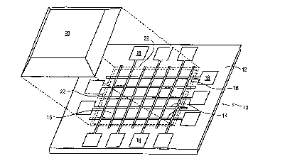
With reference now to FIG. 1, there is shown the rear side of an
electrophoretic display panel 10 as exemplified by U.S. Patent No. 4,742,345 to
DiSanto et al., this patent being incorporated herein by reference for showing
the general construction and components of an electrophoretic display panel.
The panel 10 includes a faceplate typically formed from glass which serves as a
substrate upon which is deposited a plurality of independent, electrically
conductive cathode members 14 (horizontal rows) using conventional
deposition and etching techniques. It is preferred that the cathode members 14
be composed of Indium Tin Oxide (ITO) as set forth in U.S. Patent No.
wo ss/06307 ~,63 PCT/US941~9217 ~
4,742,345. A plurality of independent grid conductor members 16 are
superposed in the horizontal over the cathode members 14 and are in~ ted
therefrom by an interstitial photoresist layer (not shown). The grid members
16 may be formed by coating the photoresist layer with a metal, such as nickel,
S using sputtering techniques or the like and then selectively m~ckin~ and etching
to yield the intersecting but insulated configuration shown in FIG. 1. Each
cathode and grid member 14, 16 termin~tes at one end of a cont~ct pad 18 or
is otherwise adapted to permit connection to display driver circuitry, which
circuitry will be described later. An anode cap 20 is sealably affixed to the
faceplate 12 and over the cathode and grid members 14 and 16 to form an
envelope for cont~ining the dielectric fluid/pigment particle suspension. The
anode cap 20 is formed from an insulating material, such as glass, and has an
inner surface coating of conductor material to form the anode. Thus by
applying voltages to the cathode and grid members 14 and 16 and the anode
20, suspended pigment particles in the dielectric fluid can be made to
~ccum~ te near, or disperse from, the intersections of selected cathode and
grid members 14 and 16 to translate these voltages into a visible display.
The discrete cathode and grid members 14 and 16 of the
electrophoretic display 10 can assume a variety of voltages during operation forcontrolling the display operations or erase, hold and write at the numerous
points of intersection defining a cathode/grid matrix. A workable panel would
have a large number of intersections, e.g., 2,200 X 1,700 or a total of 3,740,000
separately addressable intersection points. For ease of illustration, however, asmall set of intersections are shown in FIG. 1 and only a single intersection isdepicted in the rem~ining figures. The dimensions of the respective elements
have also been greatly enlarged for illustration and are not necessarily in
proportion to an actual operational device. Representative illustrations of
~ WO95/06307 - 70~...63 PCT/US94/09217
electrophoretic displays, their components and electrical circuitry can be seen
by re~erring to U.S. Patent Nos. 4,742,345 and 4,772,820, each being awarded to
- the inventors herein and which are incorporated by reference herein.
As one can readily ascertain upon reference to the previously
cited patents, the pigment at the intersections of selected rows and columns is
forced out of wells associated therewith (not shown) by selectively applying
voltages to the rows and columns, thereby exposing the dye solution and
m~king such intersections dark. The removal of the pigment from the wells is
not instantaneous but requires a period of time, which depends upon the
dimensions of the display, the applied voltages, and the properties of the
suspension. Applying a potential for too short a period of time to a grid and
cathode line intersection results in incomplete removal of pigment from the
well at that intersection. Accordingly, a pixel intensity which is less than full
black may be obtained by utilizing a scan time which is less than the scan time
required to completely remove the pigment from the wells. This escenti~lly is
the basis of the present application and such techniques for accomplishing this
will be further described.
Referring to FIG. 2, there is shown a top view of a typical X-Y
matrix consisting of cathode lines which are arranged in the horizontal plane
and grid lines which are perpendicular to the cathode lines and inc~ ted
therefrom. Thus, there are shown in FIG. 2 four cathode lines design~ted 22,
24, 2~, and N. It is, of course, understood that the number of cathode lines in
the Y direction may consist of hundreds of thonc~n(lc, depending upon the size
of the display. As indicated, insulated from the cathode lines and
perpendicular thereto, there are also shown four grid lines, 28, 30, 32, and X.
It should also be understood that there can be many more grid lines associated
with a typical display.
WO 95/06307 2~1 ~ 0 ~ 6 3 PCT/U594109~17
As seen in FIG. 2, each cathode line has a suitable driving
amplifier circuit shown in modular form and indicated by reference numerals
36, 38, 40, and 42. In like manner, each grid line has a suitable driving
amplifier referenced by modules 44, 46, 48, and 50. The driver amplifiers are
5 fabricated by typical integrated circuit techniques and may, for example, be
CMOS devices, all of which are well known and many of which are available as
conventional integrated circuit chips.
As in the case of prior art EPID displays, the display of the
present invention can typically be operated in an erase mode, a hold mode, or
10 a writing mode. In the erase mode, the anode electrode, which is not shown inFIG. 2, is placed at a negative potential while the cathodes as lines 22-N are
operated at a positive potential. In this mode, the grid lines as 28 to X are
operated at a negative potential. In the hold mode, the anode is positive while
the cathodes are held positive and the grids are again at low potential. As one
can understand from the above, the cathode operates between zero and
positive voltages. The grid operates between low and high voltages.
In the write mode, the anode is held positive while cathode lines
which are being written are placed at zero potential while non-writing cathodes
are placed at positive potential. This is the same potential employed in the
20 hold mode. In this manner, the writing grids are operated at high potential.
Thus, based on the X-Y matrix, one can produce any alpha numeric character.
As seen from FIG. 2, the Y driving amplifiers are coupled to a Y
address module 52. Essentially, the address module 52 is a well known
component and consists of various conventional decoding devices and may
25 include buffer registers and so on for the storage of data for introduction to the
various cathode lines associated with the display 10. In a similar manner, the
X driving amplifiers are coupled to an X address module 54 which module
WO95/063~7 ~6~ PCT/U594/09217
operates to provide X information for the X-Y intersections provided by the
display.
As indicated earlier, pixel intensities of less than full black can be
obtained by utilizing a scan time which is less than the scan time required to
5 completely remove the pigment from the wells. In accordance with the present
invention, therefore, a number of sequential complete image scans are required
before the displayed image will appear as a fully written picture. A readable
image may also be produced using very fast scan times and by repeated scans
can be enhanced sequentially to attain full black.
Accordhlg to the present invention, both faster writing times and
grey scale operation are made possible by selecting a scan time according to
the equation:
tS = Td/n (1)
where tS is the fixed duration for which a voltage is applied to a given pixel
intersection or scan time, n is the number of shades of grey desired, and Td is
the minimum amount of time required to remove pigment particles from the
pixel location and thus fully write that pixel full black. By way of illustration, if
the total time needed to write a display pixel full black is 80 rnilliseconds, then
it is possible to achieve eight shades of grey by selecting a scan time of 10
20 milliseconds. It will, however, be appreciated that any scan time which is less
than the minimnm full black scan time may be utilized in accordance with the
present invention. Thus, using the same example, if only two shades are
desired, it is contemplated that a scan time of 60 milliseconds may be used
even though the total scan sequence of 120 milliseconds exceeds the minimum
25 scan time.
FIG. 2 illustrates one possible arrangement for operating the
display of the present invention in accordance with a keyboard mode. As
WO 95t06307 ?.~3 PCT/US94/09217
shown in FIG. 2, information is input by keyboard 56 into the memory 60 of
co~ uler microprocessor 58. A pulse generator 62, which is coupled to X-
address module 54 and Y-address module 52, provides write pulses of a
predetermined fraction of the total write time Td, which predetermined fraction
is selected as discussed above to achieve the desired number of grey scale
levels. In accordance with the illustrative embodiment, one or more key
strokes may be utilized to define ASCII codes which correspond to particular
grey scale values. These codes are utilized by a line select grey code module
64, which may be part of microprocessor 58, to selectively address those lines
of the display cont~ining characters which are to appear darker than the other
characters.
The character data is converted into a bit stream which is
received by shift registers within the X and Y address modules. All portions of
the image are written during this first image scan. However, those portions of
the image which are to be at the lightest shade of grey are written only during
this first image scan. Selected cathode lines, as 22, 24, 26, and N, are placed at
the enable voltage level by the cathode driving amplifiers, which driving
amplifiers are fed row information by the Y address module of the
microprocessor. The column information for row 22 is fed into a shift register
within X address module 54, the output of the shift register feeding the grid
driving amplifiers. When a clock signal has shifted enough bits for one
character width, a signal is sent to the memory telling it to present the code for
the next character to the input of the character generator. This process
continues until all of the column information for cathode line 22 has entered
the grid driving amplifiers by way of the shift register. This process is repeated
for all the cathode lines such as 24, 26, and N until all characters of the display
are written.
W095/06307 170~63 PCT/U594/09217
As indicated above, the total number of scans is determined as a
function of the number of grey scale levels desired. Accordillgly, only those
characters of the display which are at the second lightest shade of grey or
darker, as determined by the microprocessor within the character generator,
are now written during a second scan. Accordingly, in this second scan the line
selecl: grey code module 64 feeds the row and colnmn information of the
display into the shift registers of the X and Y address modules, but, as alreadyin~lic~ted, the row and column information corresponding to those pixels at the
lightest shade of grey is omitted. Thus, by operation of the line select module
64, only those rows and columns which contain characters of the second lightest
shade or darker are energized by the pulse generator. Sequential sc~nning
procedure is continued for shades three, four, five, six, and seven. Only those
portions of the image which are black are scanned on all eight sequential scans.Hence, in this manner as one will readily understand, all pixels of
the display can be written into during a first scan, with only successively darker
pixels being written into during subsequent scans. Accordingly, not only does
the present invention make it possible to achieve grey scale operation, but it
also permits a readable image to be displayed in si~nifi~ntly less time than is
taught by prior art EPIDs. It should thus be apparent to those skilled in the
art that the above-described techniques and associated apparatus lends itself tomany alternate embodiments. For example, instead of operating the display in
a keyboard mode, the display may be adapted to receive data from a typical
telephone line or other tr~n~mi~ion media using an analog to digital converter
and digital signal pixel generator (not shown). Each of the aforementioned
components are commercially available and well known in the prior art, all of
which are deemed to be encompassed within the spirit and scope of the
specification and the claims as appended.