Note: Descriptions are shown in the official language in which they were submitted.
WO 95J08153 PCT/US94/10312
-1-
SCAN TEST CIRCUIT USING FAST
TRANSMISSION GATE SWITCH
BACKGROUND OF THE INVENTION
1. Field of the Invention
The invention relates generally to the testing of
electronic systems, comprising integrated circuits that are
interconnected to each other, and more specifically to test
circuits that include scan cells used to test such
integrated circuits and interconnections.
2. Description of the Related Art
In the past, integrated circuits (ICs) have been
tested by performing a complete boundary scan. Each pin
was physically accessed and tested, one pin at a time.
However, as the dimensions of ICs have decreased, it has
become increasingly difficult to physically access IC pins
for testing. As a result, serial testing methods have been
developed. In particular, the Joint Test Action Group
Standard (JTAG) was formed and has adopted as a formal IEEE
standard, IEEE 1149.1.
The standard requires that an IC include several
dedicated pins used for testing. The pins control a serial
data path on the IC that provides access to the IC's
functional input/output (I/O) structure. Scan cells are
disposed along the serial path, one for each I/O pin. Data
may be "sensed" or read from any of the IC's functional I/O
pins and stored in a corresponding scan cell. The stored
values then can be serially shifted out of the IC for
examination. Alternatively, the scan cells may also be
serially loaded with data values, and the I/O pins then may
be "forced" to the values in the scan cells. Thus, inputs
and outputs may be forced to certain desired values during
testing.
WO 95/08153 PCT/LTS94/10312
_2_
The IEEE 1149.1 Standard has been implemented on
application specific integrated circuits (ASICs) as well as
on basic logic ICs. However, the IEEE 1149.1 standard
still is offered on relatively few ICs. This has posed
problems for developers attempting to test subsystems of
ICs and interconnects on printed circuit boards, for
example.
A subsystem of ICs on a printed circuit board, for
example, may be tested in accordance with the IEEE 1149.1
standard if every IC in the subsystem that accepts inputs
to the subsystem and every IC providing outputs from the
subsystem has the circuitry necessary to implement testing
in accordance with the standard. However, not all ICs have
the scan circuitry required to make them IEEE 1149.1
compliant.
One solution to this problem is to use IEEE 1149.1
compliant buffers in the subsystem. The inputs and outputs
of these buffers can be forced or sensed as they pass
through the buffer. Buffers have been available in the
past for this use. For example, there is the 8244 buffer
produced by Texas Instruments, the SCAN 18244 produced by
National Semiconductor, and the QS 618 244 produced by
Quality Semiconductor, the Assignee herein.
While these earlier IEEE 1149.1 complaint buffers
generally have been acceptable, there have been
shortcomings with their use. In particular, for example,
the buffers may draw power, and in many applications this
power penalty may be significant. Also, often there is a '
speed penalty; the buffers introduce a delay into the
system. At times the circuit board may have to be '
redesigned to account for the delay. Furthermore, some
applications may require data to flow bidirectionally
between subsystems. For such applications, a bidirectional
switch that is largely passive when closed is desirable.
WO 95/08153 PCT/US94/10312
-3-
Thus, there has been a need for an IEEE 1149.1
compliant buffer that is bidirectional, has low power
consumption and introduces little if any delay. The
present invention meets this need.
SUflNlARY OF THE INVENTION
In order to overcome the above-discussed disadvantages
of known test methods, one aspect of the present invention
relates to a fast transmission integrated circuit buffer
device with scan cells. The buffer device has two
input/output nodes and is operative to pass or block the
bidirectional transmission of external data signals between
the nodes. The switching device comprises a bidirectional
field-effect transistor with a first terminal connected to
a first input/output node, a second terminal connected to a
second input/output node, and a gate terminal. The
transistor passes bidirectional external data signals
between the input/output nodes when the transistor is
turned on and blocks the passage of external data signals
when the transistor is turned off.
Scan cells are connected to each input/output node and
are operative to sense and store from, or force data
signals to the input/output nodes. The stored data signals
may be serially shifted through the scan cells and out a
test data output node for testing and examination.
Another aspect of the present invention relates to
using a fast transmission integrated circuit switching
device for testing subsystems and interconnects on a
printed circuit board. Since the buffer device comprises a
bidirectional field-effect transistors with the above-
specified dimensions, it has minimal power consumption and
time delay. Further, the device can be implemented as a
stand alone device which is well suited for selective
placement on a printed circuit, for example, board for
WO 95/08153 PCT/US94/10312
_4_
testing where access to data signals is not already
available.
BRIEF DESCRIPTION OF THE DRAWINGS
r
These and other features and advantages of the present
invention will become more apparent to those skilled in the
art from the following detailed description in conjunction
with the appended drawings in which:
Figure 1 is a schematic circuit diagram of an earlier
passive transmission gate switch and of a driver and
receiver illustrating a conventional design of the switch.
Figure 2 is a schematic view of an earlier active
switch device using an enabled buffer and of a driver and
receiver to illustrate another conventional design.
Figure 3 is a perspective view of a MOS transistor
useful for illustrating the invention.
Figure 4 is a cross-sectional view of the transistor
of Figure 3.
Figure 5A is a schematic circuit diagram of a fast
transmission gate switch and of a driver and receiver to
illustrate a preferred embodiment of the invention.
Figure 5B is a partially cross-sectional view and
partially schematic view of the transmission gate switch of
Figure 5A.
Figure 5C is a schematic circuit diagram illustrating
in more detail one embodiment of the driver 104 of '
Figure 5B.
WO 95/08153 PCT/US9.1/10312
-5-
Figure 5D is a schematic view of the switch of
Figure 5B, illustrating in more detail the capacitances of
the switch.
Figure 5E is a conceptual circuit diagram illustrating
the RC delay experienced by a signal propagating from
node A to node B to illustrate the invention.
Figure 6 is a schematic circuit diagram of a fast
transmission gate switch and of a driver and receiver to
illustrate an alternative embodiment of the invention.
Figures 7 and 8 are schematic circuit diagrams of two
different transmission gate switches to illustrate
additional alternative embodiments of the invention.
Figure 9 is a schematic view of a bus switch for
switching signals between two sets of bus lines.
Figure 10 is a schematic circuit diagram of a bus
exchange switch.
Figures 11A, 11B are schematic circuit diagrams
illustrating the operation of the circuit in Figures 5A-5D.
Figure 12 is a block diagram of a buffer device
incorporating fast transmission gates in accordance with
the present invention.
Figure 13 is a more detailed block diagram of a
portion of the buffer device of Figure 12 showing
additional details of the control lines used to control the
scan/storage cells and showing a representative fast
transmission gate switch.
Figure 14 is a schematic diagram of a scan/storage
cell of the buffer device of Figures 12 and 13.
WO 95/08153 . PCT/ITS94/10312
-6-
Figure 15 is a block diagram showing additional
details of the control logic of the buffer device of
Figures 12 and 13.
Figure 16 is a state diagram which illustrates the
operation of the test access port of the control logic of
Figure 15.
DETAILED DESCRIPTION OF THE PREFERRED EMBODIMENT
The present invention comprises a novel method and
apparatus for the testing of electronic circuits. The
following description is presented to enable any person
skilled in the art to make and use the invention.
Descriptions of specific applications are provided only as
examples. Various modifications to the preferred
embodiment will be readily apparent to those skilled in the
art, and the generic principles defined herein may be
applied to other embodiments and applications without
departing from the spirit and scope of the invention.
Thus, the present invention is not intended to be limited
to the embodiment shown, but is to be accorded the widest
scope consistent with the principles and features disclosed
herein.
Fa$t Transmission Gate Switch
Figure 1 is a schematic circuit diagram of a
conventional transmission gate switch 20 connected to the
output of a driver 22 and the input of a receiver 24 at
nodes A, B respectively. The signal to be switched appears
at the output of driver 22. When switch 20 connects nodes
A and B, such signal is transmitted to node B and appears
at, the input of receiver 24. Driver 22 and receiver 24 may
each be part of another circuit chip package mounted on a
printed circuit board where switch 20 is connected by
conductive traces 32 through nodes A, B to these chip
packages.
WO 95/OS1S3 PCT/LTS94/10312
_7-
Switch 20 has resistance R so that the switch may be
represented conceptually as a resistor 26 in series with a
pure switch 28 as shown in Figure 1. A signal propagating
between nodes A and B will experience capacitive effects of
traces 32 connecting switch 20 and receiver 24, of the
receiver 24 and switch 20. Switch 20 is typically employed
in the form of an electronic package with pins connected to
nodes A, B. As defined on pages 705, 706 of Modern
Microelectronic Circuit Design IC Applications
l0 Fabrication Technoloctv, Vol. 2, by staff of Research and
Education Association, Dr. Folgiel, Director, Research and
Education Association, New York, New York, 1981, the
parasitic capacitance of an electronic device package with
leads or pins can be of two types, inter-lead capacitance
and capacitance from lead-to-ground. Switch 20 has three
leads, one connected to driver 22, the other connected to
receiver 24 by traces 32 on a printed circuit board, and a
third lead for the switch enable signal. There will be
inter-lead capacitances between the three leads of switch
20, and there will also be capacitances between the three
leads of switch 20 and ground.
The above-described inter-lead and lead-to-ground
capacitances of package 20, those introduced by traces 32
and other board level connections are represented
conceptually by capacitor 30 connected between node B and
ground and labeled ~~parasitic capacitance~~ in Figure 1.
Since this parasitic capacitance represented by the
capacitor is inherent in the switch, capacitor 30 is shown
in dotted lines. Obviously, the inter-lead capacitances as
well as the lead-to-ground capacitances of switch 20 would
depend on the size, geometry, material and the exact
configuration of the package 20, its leads, and of traces
32 and other board level connections. The total internal
capacitance of switch 20 is given by the total capacitive
effect of the parasitic capacitance of capacitor 30, and
the capacitance of other portions of switch 20, the value
WO 95/08153 ~ PCT/US94/10312
of which will depend on the structure of the switch.
Therefore, the total capacitance seen by a signal .
propagating between nodes A and B is given by the effects
of the internal capacitance of switch 20, the capacitance ,
of receiver 24, and the capacitance of traces 32 connecting
switch 20 to receiver 24. Thus the delay of the signal
propagating from node A to node B is caused by two RC
delays: (1) the product of the resistance R of resistor 26
and the capacitance of trace 32 connecting switch 20 and
receiver and of receiver 24, and (2) the product of the
resistance R of resistor 26 and the internal capacitance of
switch 20, including that of capacitor 30. The
second (2) product will depend on the specific structure of
switch 20, and will be omitted for now, since the first
product alone makes switch 20 unsuitable for use in high
speed switching between logic devices, as will be clear
from the discussion below.
In typical printed circuit board designs for computer
and logic applications, a typical capacitance of the bus
(e. g., that of trace 32, of receiver 24 and other
associated circuitry whose capacitance effects will be felt
at node B) downstream from switch 20 is about 50 pF.
Therefore, if switch 20 has a large resistance value, the
RC time constant resulting from such resistance and the
typical bus capacitance of 50 pF will be large, resulting
in a significant signal delay when the signal propagates
from A to B. The propagation delay introduced by the
switch is therefore at least equal to the value of the RC
time constant. A standard transmission gate switch is the
CMOS 4016 integrated circuit. The typical resistance
values of existing transmission gate switches such as the
4016 are in the range of 250-1,000 ohms. This type of
switch would therefore introduce at least a delay of the
order of 12-50 nanoseconds, assuming a 50 pF bus
capacitance. Such delay is unacceptable for switching high
speed signals required in many computer and logic
WO 95/08153 PCT/US94/10312
_9_
applications. For this reason, the 4016 type switch is
more commonly used in analog circuits and seldom in board
level computer or digital logic designs. For the latter
applications, active logic devices such as industry
4
standard 74F244 buffers have been used such as shown in
Figure 2. To simplify the discussion, identical components
and the figures of this application are identified by the
same numerals.
As shown in Figures 1 and 2, transmission gate switch
has been replaced by a logic buffer 40 in Figure 2.
Driver 22 and receiver 24 may be part of computer or logic
chip packages mounted on a printed circuit board and
connected to buffer 40 by conductive traces 32 on the
15 board. Buffer 40 is also in the form of a package having
inter-lead and lead-to-ground parasitic capacitance, whose
values may be different from those of switch 20; for this
reason, such parasitic capacitance of buffer 40 are
represented by capacitor 30', also shown in dotted lines.
20 Buffer 40, however, introduces a delay of its own because
of the inherent speed limitations of active logic. The
74F244 buffer driving a 50 pF load introduces a delay of
about 6.5 nanoseconds. Thus while using a logic buffer 40
to replace switch 20 does reduce the delay in signal
transmission, it is difficult to further reduce the delay
introduced by the buffer itself. It is therefore desirable
to provide an improved switching device where the above-
described difficulties are alleviated.
Figure 3 is a perspective view of a fast transmission
MOS transistor used in a present embodiment of a buffer
circuit in accordance with the present invention. Figure 4
is a cross-sectional view of the transistor of Figure 3.
As shown in Figures 3 and 4, the channel length of a MOS
type transistor is the distance L between the source and
drain regions of the transistor while the channel width is
the dimension W of the transistor in the direction where
WO 95/08153 ., PCT/US94/10312
-10-
the cross-sectional configuration of the transistor does
not change. Another common definition of the channel
length is the width of the gate that overlaps the active
region of the transistor between the source and drain.
Another common definition of the channel width is the
length of the gate overlapping the active region of the
transistor between the source and drain.
Figure 5A is a schematic circuit diagram of a fast
transmission gate switch and of a driver and receiver
suitable for use in a buffer device in accordance with the
invention. As shown in Figure 5A, the transmission gate
100 includes a N-channel MOS transistor 102 and a driver or
gate 104 for controlling the gate of transistor 102 in
response to an external signal from node C. The channel
length of transistor 102 is preferably less than 1.5
microns, and in some applications preferably less than 1
micron. The channel width of transistor 102 is preferably
more than 1,000 microns and in some instances preferably
1,200 microns or more. In reference to Figures 3 and 4, by
reducing the channel length, the resistance of the resistor
is reduced since current carriers have a shorter distance
to travel in order to conduct current between nodes A, B.
By using a transistor with large channel width compared to
the transistors in the 4016 type gate, the resistance of
transistor 102 is further reduced in comparison. With the
above-described design for transistor 102, it is found that
the inherent resistance of transmission gate switch 100
between nodes A, B when the transistor 102 is turned on
(on-resistance) can be reduced to a value of less than
10 ohms, although a value of less than 50 ohms may be °
suitable. Applicant has discovered that in some designs,
the resistance of switch 100 when transistor 102 is turned '
on may be reduced to a value of less than 5 ohms. Shorter
channel lengths also result in reduced capacitance of
transistor 102. The internal capacitance of the switch 100
WO 95/08153 PCT/US94/10312
-11-
a
and its effect on signal delay will be discussed in more
detail below in reference to Figures 5B-5E.
Figure 5B illustrates in more detail the structure of
fast transmission gate switch 100 of Figures 5A. In
Figure 5B, a partial cross-sectional view of a portion of
transistor 102 is shown. Transistor 102 includes a gate
112, drain 114, source 116, and substrate 118 where the
gate is separated from the drain and source and substrate
by an insulating layer 120. Drain 114 is connected through
a conductor 122 through a package body (not shown) of
switch 100 to an input/output pin (shown symbolically) at
124. Similarly, source 116 is connected through a
conductor 126 through the package body (not shown) to
input/output pin 128. Pin 124 is connected to node A of
Figure 5A through trace 32 and pin 128 is connected to node
B by means of another trace 32. The output of driver 104
is connected to gate 112 through node 130. The driver
receives the switching signal from node C through pin 132.
In reference to Figures 5A, 5B, the inter-lead parasitic
capacitance of switch 100 would be the capacitances between
pins 124, 128, 132 and the lead-to-ground parasitic
capacitances of switch 100 would be the capacitances of
pins 124, 128, 132 to ground. In addition to experiencing
such capacitances, a signal passing between pins 124, 128
will also experience the effects of the capacitances
between gate 124 on the one hand and the drain 114 and
source 116 on the other, as well as capacitances between
drain 114, source 116 and substrate 118, referred to as the
capacitance of the transistor. The internal capacitance of
the switch 100 is given by the total capacitive effects of
the capacitance of the transistor and the parasitic
capacitance of the switch consisting of the inter-lead and
lead-to-ground capacitances and represented by capacitor
30~~ in Figure 5A.
WO 95/08153 PCT/US94/10312
_12_
The most important components of the above-enumerated
capacitances are the lead-to-ground capacitances and the
gate to drain and source capacitances. For many commonly
used packages, total capacitive effects of the inter-lead
and lead-to-ground capacitances are of the order of 8 or 10
pF experienced by signals transmitted through the leads of
the package. In one implementation of transistor 102, the
gate to drain and source capacitances amount to about 1 or
2 pF and each of the lead-to-ground capacitances of pins
124, 128, 132 amount to about 4 pF. As indicated in the
1991 Data Book, pages 5-24, by Quality Semiconductor, Inc.,
assignee of the present application, the on internal
capacitance of a switch having characteristics similar to
that of switch 100 is about 10 pF and its off capacitance
is about 6 pF. Thus when transistor 102 is turned off, the
internal capacitance seen at either pin 124 or 128 will be
the gate to drain and source capacitance and the lead-to-
ground capacitance of that particular pin. Whereas if the
transistor 102 is on, the internal capacitance seen at
either pin would also include the lead-to-ground
capacitance of the other pin as well. For this reason, the
internal capacitance of switch 100 seen at either pin 124
or 128 will be higher when the transistor is on compared to
that seen when the transistor is off. Typically, substrate
118 is connected to ground and node 130 at the output of
driver 104 is at a stable DC potential when the transistor
is not being turned on or off.
Figure 5C is a schematic circuit diagram illustrating
one embodiment of driver 104. As shown in Figure 5C,
driver 104 is an invertor comprising a P-channel transistor '
142 and an N-channel transistor 144 connected in parallel
between switching pin 132 (switching pin of switch 100) and
node 130. As also indicated in Figure 5C, the two
transistors are connected to a power rail VCC and ground as
usual. While the driver 104 is shown as an invertor, it
will be understood that other driver or gate configurations
WO 95/08153 PCT/L1S94110312
-13-
may be 'used, such as NOR- or NAND-gates. Since the
parasitic capacitance for switch 100 may be different from
those of switches 20 and 40, the capacitor in Figure 5A is
labeled 30" to show that it may be different from those of
switches 20 and 40.
Figure 5D is a schematic view of the fast transmission
gate switch 100 illustrating in more detail some of the
more significant capacitances in the switch. Thus, the
lead-to-ground capacitances of lead 124 is illustrated by
capacitor 162 shown in phantom, and the lead-to-ground
capacitance of lead 128 is illustrated by capacitor 164
shown in phantom. The gate to drain and gate to source
capacitances are shown in phantom as capacitors 166, 168.
In the implementation indicated above and in the 1991
Data Book of Quality Semiconductor, Inc., the capacitance
of switch 100 when the transistor is on is about 10 pF.
Hence, the propagation delay caused by the resistance and
internal capacitance of the switch, assuming a resistance
value between pins 124 and 128 of about 5 ohms, is about
0.05 nanoseconds. If the bus capacitance is 50 pF, then
the RC delay caused by the switch resistance of about
5 ohms and bus capacitance of 50 pF is about
0.25 nanoseconds, so that the total delay seen by a signal
propagating through the switch to reach the receiver is
about 0.3 nanoseconds, well below the 6.5 nanoseconds delay
caused by the typical conventional buffer.
Figure 5E is a conceptual circuit diagram illustrating
the RC delay experienced by a signal propagating from node
A to node B. Thus, in reference to Figure 5E, the
resistance of transistor 102 is R;. The internal
capacitance of the switch is C; and the bus capacitance is
Cb, where the resistor and the two capacitors are shown in
phantom since they represent the respective resistance and
capacitances of the switch and bus and are not real circuit
WO 95/08153 PCT/US94/10312
_1,~_
elements. Then the total RC delay caused by the switch as
seen by a signal propagating from node A to node B is given
by R; (C; + Cb) . As long as this total delay R; (C; + Cb) caused
by the switch 100 is less than the typical delay caused by
the buffer of 6.5 nanoseconds for a 74F244 buffer driving a
50 pF load, it is advantageous to replace the buffer by the
switch of this invention. Thus, for any given bus
capacitance Cb, R; and C; are chosen so that the total delay
R;(C; + Cb) caused by the switch 100 is less the typical
delay caused by the buffer.
The above-described transmission gate switch 100 may
be used advantageously to replace active logic devices such
as 74F244, 74F245 for switching high speed digital logic
signals in a board level design. The replacement of the
active device with device 100 will greatly reduce the
propagation delay, logic noise (e. g., "ground bounce"
noise) and power dissipation associated with the active
device replaced. Please see the "Application Note AN-O1"
of the 1991 Data Book of Quality Semiconductor, Inc.,
Switch 100 is also inherently bi-directional. Other
embodiments of the switch described below in reference to
Figures 5-8 also have similar advantages.
The fast transmission gate switch 100 may be modified
by replacing transistor 102 by a P-channel transistor where
the polarity of the signal for controlling the gate of the
transistor has been adjusted if necessary to accommodate a
P-channel device. Where the P-channel device also has the
above-described channel lengths and widths, switch 100 may
be constructed to have a on-resistance of not more than
10 ohms.
The gate of transistor 102 is controlled by the output
of a driver 104 which may include a pair of P-channel and
N-channel resistors connected in parallel between node C
and the gate of transistor 102. In order to increase the
WO 95/08153 PCT/ITS94/10312
_15_
speed of switching, the pair of transistors in driver 104
would preferably each have a channel length of 1.5 microns
or less and channel widths greater than 200 microns. Where
a driver 104 and transistor 102 are fabricated as a stand-
s alone integrated circuit device 100 using the same
fabrication technology, the transistors in device 100 may
be grown so that all the transistors in the device have
short channel lengths. Where device 100 is fabricated as
an integrated circuit, it can be made in the form of a
package having five pins for connection to nodes A, B, C,
and to power and ground.
Figure 6 is a schematic circuit diagram of a fast
transmission gate switch and of a driver and receiver to
illustrate an alternative switch suitable for use in the
invention. As shown in Figure 6, switch 150 includes a
pair of N-channel transistor 102 and a P-channel transistor
152 connected in parallel between nodes A, B. The gate of
transistor 102 is controlled by a driver 104 as in Figure 5
and the gate of transistor 152 is controlled by the output
of the driver 154 whose input is connected to the output of
driver 104. Where both transistors 102, 152 have the
channel lengths and widths as those described above for
transistor 102, the on-resistance of switch 150 would be
10 ohms or less.
Figures 7 and 8 are schematic circuit diagrams of two
different fast transmission gate switches to illustrate
additional alternative switches suitable for use in the
invention. Bipolar transistors typically have
on-resistances of less than 10 ohms so that they may be
used instead of MOS transistor 102. Such configuration is
illustrated in switch 200 of Figure 7. While a npn
transistor 202 is employed in switch 200, it will be
understood that a pnp type transistor may be used instead
and is within the scope of the invention. As shown in
Figure 7, the base of transistor 202 is controlled by the
WO 95/08153 PCT/US9~/10312
-16-
output of a driver 204 through resistor 206. Driver 204
may be one of the 7400 TTL series of logic gates, such as
the 74F04 gate.
In Figure 8, a back to back connection of two npn
transistors 202 and 252 are shown for switch 250, although
2 pnp transistors may be used instead. It is known that
for a bipolar transistor, unlike a MOS transistor, the
current flowing between the collector and emitter is
greater in one direction than the other. By placing two
transistors 202, 252 in two parallel paths and connected to
nodes A, B so that each node is connected to a controller
of one transistor and the emitter of the other transistor
(anti-parallel arrangement), currents will flow through the
path of lesser resistance in each direction so that the
amount of current that needs to be pumped through the
switch is reduced.
Figure 9 is a schematic circuit diagram of a CMOS
switch device employing multiple transistor switches for
switching signals between two sets of data lines. Quality
Semiconductor, Inc., of Santa Clara, California, assignee
of the present application, has employed a switch device
like that shown in Figure 9 as a bus switch in product
74FCT3384. As shown in Figure 9, switch device 500 is a
high speed TTL bus connect device. When enabled, the bus
switch device directly connects two buses with the
connection resistance of less than 5 ohms. The five lines
A0, A1, A2, A3, A4 in bus A are each connected through a
transistor 102 to the bus lines B0, B1, B2, B3, B4
respectively. The five transistors 102 connecting AO-A4 to
BO-B4 have their gates controlled by the output of driver
104'. Similarly, the five lines A5-A9 in bus A are
connected to the respective one of the five bus lines B5-B9
in bus B through transistors 102 whose gates are controlled
by the outputs of a driver 104 " . Thus switch device 500
includes ten switches 102 arranged as two banks of five and
WO 95/08153 PCT/LTS94/10312
-17-
controlled by two different drivers. This allows switch
device 500 to be used as a 10-bit switch or as a 5-bit,
2-to-1 multiplexer. This is accomplished by electrically
connecting the pairs of lines BO-B5, B1-B6, B2-B7, B3-B8
and B4-B9. In such event, when the output of driver 104'
is high, the signals present on lines AO-A4 will be
transmitted to the B bus whereas if the output of driver
104°' is high, the signals present on lines A5-A9 will be
transmitted to the B bus instead to accomplish the 2-to-1
multiplexer function. When the output of one of the two
drivers is low, the transistors driven by the driver will
be turned off and the respective bus lines connected by
such transistors will be disconnected from one another.
The above-described function is summarized in the Function
Table below.
Function Table:
BEA BEB B O - 4 B S -- ~ Funct.~.
on
H H Hi-Z Hi-ZDisconnect
L H AO-4 Hi-ZConnect
H L Hi-Z A5-9Connect
L L AO-4 A5-9Connect
Device 500 includes in essence ten switches, where
each switch includes an N-channel MOS transistor driven by
a CMOS gate. When the switch is enabled, the gate of the
N-channel transistor is at Vcc (+5 volts) and the device is
on. These devices have an on resistance of less than 5
ohms for voltages near ground and will drive in excess of
64 mA each. The resistance rises somewhat as the I/O
voltage rises from a TTL low of 0.0 volts to a TTL high of
2.4 volts. In this region the A and B pins are solidly
connected, and the bus switch is specified in the same
manner as a TTL device over this range. As the I/O voltage
WO 95/08153 PCT/US94/10312
_18_
rises to approximately 4.0 volts, the transistor turns off.
This corresponds to a typical TTL high of 3.5 to 4.0 volts.
Figure 10 is a schematic circuit diagram of a CMOS bus
exchange switch 600 in another product 74FCT3383.
Switch 600 comprises two banks of ten switches arranged to
gate through or exchange two banks of five signals. This
allows switch 600 to be used as a 10-bit switch or as a
5-bit, two-way bus exchange device. Switch 600 is
particularly useful for exchange and routing operations
such as byte swap, crossbar matrices, and RAM sharing. The
functions of switch 600 are summarized in the Table below.
Function Table:
BE $x 80-8 gl-~Fur3.ctioi~
H X Hi-Z Hi-ZDisconnect
L L AO-8 A1-9Connect
L H A1-9 AO-8Exchange
The bus switch provides a path for a driving device to
drive capacitance to ground and to drive capacitance up
from ground. This is shown in Figures 11A, 11B. When the
A (or B) input is driven to a TTL low of 0.0 volts, the
N-channel transistor is fully on and the B (or A) output
will follow it. Likewise, when the A (or B) input is
driven from a TTL low of 0.0 volts, the switch is fully on
and the B (or A) output will follow it through threshold
and beyond. This means that the rise and fall time
characteristics and waveforms of the B (or A) output will
be determined by the TTL driver, not the bus switch. The
switch introduces insignificant propagation delay.
When the bus switch is disabled, the N-channel
transistor gate is at 0.0 volts, and the transistor is off.
By the nature of the N-channel transistor design, the A and
WO 95/08153 PCT/US94/10312
-19-
B pins are fully isolated when the transistor is off.
Leakage and capacitance is to the chip substrate (i.e.,
ground) rather than between input and output. This
minimizes feedthrough in the off state. Because only an
N-channel transistor is used, either A or B pins) can be
taken to Vcc and above, and the device can be powered down
without loading either bus.
The above-described fast transmission gate switches
have both low on resistances and internal capacitances as
well as fast turning on and off times. Where the
transistors in the drivers 104 (and of drivers 104', 104 " )
have channel lengths of 1.5 microns or less and channel
widths of 200 microns or more, and the gate to drain and
source capacitances of transistor 102 are of the order of 1
or 2 pF, transistor 102 can be turned on or off upon the
application of a switching signal to node C in a just a few
nanoseconds, in any event less than 7 nanoseconds.
Buffer Device in Accordance with IEEE 1149.1 Standard
Incorporating Fast Transmission Gate Switch
Referring to the illustrative drawing of Figure 12,
there is shown a block diagram of an integrated circuit
buffer device 800 in accordance with the present invention.
The device is constructed to meet the requirements of the
IEEE 1149.1 standard. Thus, the overall architecture is
not novel, and no claim is made to the overall architecture
per se. However, the use of fast transmission gate
switches to selectively interconnect scan cells in an IC
constructed is not taught by the IEEE 1149.1 standard.
The buffer device 800 includes a number of data pins
A0, A1, A2 ... An and B0, B1, B2 ... Bn. Data pins
AO ... An are disposed along one side of the device, and
data pins BO ... Bn are disposed along the other side.
Multiple fast transmission gate switch transistors/
register latch circuits 802-0 through 802-n are disposed
WO 95/08153 PCT/US94/10312
_20_
within the device. A fast transmission gate switch
transistor within circuit 802-0 can be used to selectively
open or close the data path between data pin AO and data
pin B0, for example. Similarly, a fast transmission gate
switch transistor within circuit 802-1 can be used to
selectively open or close a data path between data pin A1
and B1, and a fast transmission gate switch transistor
within circuit 802-n can be used to selectively open or
close a data path between data pin An and data pin Bn.
Multiple data scan/storage cells 804-AO ... 804An and
804-BO ... 804Bn are disposed within the device. The
scan/storage cells can be used to sense data on respective
data pins or to force data onto respective data pins. In
the present embodiment, there is a storage cell for each
data pin. Scan/storage cell 804-AO can be used to sense
data on data pin A0; or it can be used to force a data
value onto data pin A0, for example. Likewise,
scan/storage cell 804-Bn can be used to sense data on data
pin Bn; or it can be used to force a data value onto data
pin Bn. Thus, there are 2n scan/storage cells for the 2n
data pins. Each data cell can store digital data which is
sensed on a respective data pin or can force digital data
onto a respective data pin. The respective data pins and
the respective scan/storage cells can be operationally
connected on a serial digital path 806 which extends from
test input pin 808 to test output pin 810.
In operation, the buffer device 800 can be disposed
between two external devices 830 and 840. For example, the
data pins on one side of the device AO ... An can be
connected to terminals of a first device to be tested 830.
The data pins on the other side of the device 800 can be
connected to data pins of the second device under test 840.
During non-test mode operation, the fast transmission
gate switches within circuits 802-0 through 802-n are
WO 95/08153 PCT/ITS94/1~312
-21-
closed, and the serial data path 806 is non-operational.
Digital information can be communicated bidirectionally
between the first external device 830 and the second
external device 840.
During test mode operation, the fast transmission gate
switches within circuits 802-0 through 802-n can be opened.
The serial data path 806 can be used to serially shift test
data into the various scan/storage cells to force data onto
corresponding data pins, for example. Specifically, for
example, digital information loaded into scan cell 804-A2
can be used to force a desired digital value onto data pin
A2. Specifically, if the switch in circuit 802-n is
opened, then the value in cell 804-A2 can be forced onto
data pin A2 but not onto pin B2. The response of the first
external device 830 to the digital value forced onto pin A2
then can be observed.
Alternatively, for example, the first external device
830 can be operated, and at appropriate time junctures, the
data on data pins AO ... An can be sensed and loaded into
respective scan cells 804-AO through 804-An. That data
then can be serially shifted out on the serial digital path
806 via output test terminal 810 for evaluation. The
switches in circuits 802-0 through 802-n can isolate the
data pins AO ... An from data pins BO ... Bn. If the
respective switches in circuits 802-0 through 802-n are
opened when the data on data pins AO ... An are sensed,
then any data values on data pins BO ... Bn will not
influence the data values sensed and scanned into cells
804-BO through 804-Bn.
In the test mode data can be serially shifted from a
test data input terminal 808 into the scan cells. For
example, a data bit could be shifted in sequence first to
cell 804-An, then to cell 804-An-1 and ultimately, on to
cells 804-A1, 804-A0, and from there, it could be shifted
WO 95/08153 PCT/US94/10312
-22-
in sequence from cell 804-BO to cell 804-Bn. When the data
bit arrived at cell 804=Bn it then could be used to "force"
a value onto data pin Bn. Alternatively, for example, a
data bit sensed at data pin A1 and stored in cell 804-A1
could then be shifted in sequence to cell 804-AO and on to
cells 804-BO through 804-Bn whereupon it could be shifted
out onto the data output terminal 810.
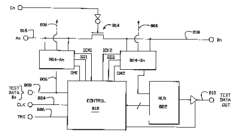
Also shown in Figure 12 is control logic 812 used to
control the operation of the serial digital path and the
operation of the scan/storage cells. Referring to
Figure 13, there is provided a more detailed block diagram
showing the interconnection of the control logic 812 with
scan cells 804-An and 804-Bn and a representative fast
transmission gate switch 814. It will be appreciated, of
course, that the overall operation of the entire digital
path and the remainder of the scan/storage cells will be
appreciated from the explanation of the operation of scan
cells 804-An and 804-Bn and the operation of switch 814
shown in Figure 13.
Figure 13 illustrates the use of a fast transmission
gate switch 814 in a buffer device 800 that meets the
requirements of IEEE 1149.1. The switch is responsive to
at least one external on/off control signal applied at Cn,
and includes a first input/output node An and a second
input/output node Bn. The switching device is operative to
pass or block the bidirectional transmission of external
data signals between the node An and the node Bn. The
switching device 800 comprises a bidirectional fast
transmission gate field-effect transistor 814 including a '
first input/output terminal and a second input/output
terminal and a gate terminal. Terminal An is connected to '
data path 816 and terminal Bn forming a second data path
818. The transistor passes bidirectional external data
signals between pins An and Bn when the transistor 814 is
turned on and blocks the passage of external data signals
WO 95/08153 PCT/US94/10312
"~'~~rw _23_
,(l' ~
between pins An and Bn when said transistor 814 is turned
off .
An external terminal Cn for receiving the at least one
external on/off control signal and a driver circuit 820
provide an internal on/off control signal to the gate
terminal of the field-effect transistor 814.
In accordance with IEEE 1149.1, a first scan/storage
cell 804-An is connected to the first data pin An and is
operative to sense and store data signals from data pin An.
A second scan/storage cell 818 is connected to the second
data path 818 and is operative to sense and store data
signals from said second data pin Bn.
The first embodiment of the present invention also
comprises a test data input node 808 and a test data output
node 810. The scan/storage cell means 804-n receives data
from the test data input node 808. The scan/storage cell
804-Bn is connected to the test data output node 810 via
multiplexes 820. The multiplexes 820 allows the
scan/storage cell 804-Bn to be bypassed and other signals
to be output through test data output node 810.
As described above, each scan cell has at least two
modes of operation, a sense mode and a shift mode. When
operating in sense mode the scan/storage cell 804-An senses
and stores data signals from the first data pin An, and the
second scan/storage cell 804-Bn senses and stores data
signals from the second data pin Bn.
A clock signal is provided to the control logic 812
through the test clock node 824 and a test mode select
signal is provided to the control logic means through the
test mode node 826. The control logic means generates and
provides an internal clock signal ICK1, ICK2 and a shift
select signal SS1, SS2 to each scan/storage cell 804-An
WO 95/08153 PCT/LTS94110312
_24_
through 804-Bn. Each scan cell means senses and stores a
new data signal only during transitions in its respective
internal clock signal ICK1, ICK2, and each scan cell
operates in shift mode only when its respective shift
select signal SS1, SS2 has a predetermined shift value. In
the preferred embodiment, the shift value is a low voltage
or logical "0" applied to the scan cell means.
The scan cell may also be used to force data values on
the data paths. Each scan cell has an output data value,
and the control logic generates and provides an output mode
signal OM1, OM2 to each scan cell.
Scan cell 804-An forces data pin An to have a data
value equal to the output data value of scan cell 804-An
when that scan cell's output mode signal has a
predetermined force value. In the preferred embodiment,
the force value is a high voltage or logical "1" applied to
the scan cell.
Similarly, scan cell 804-Bn forces the data pin Bn to
have a data value equal to the output data value of scan
cell 804-Bn that when scan cell's output mode signal has a
predetermined force value. In the preferred embodiment,
the force value is a high voltage or logical "1" applied to
the scan cell.
Thus, depending upon the internal control signals
generated by the control logic 812, the scan cell may be
serially loaded with data from the test data input node, or
may sense and store data from their respective data paths. '
The data stored in the scan cells may also be serially
shifted out the test data output node and the scan cell's
output values may be used to force the data paths to the
same data value.
WO 95/08153 PCT/US94l10312
-25-
The implementation of the scan cells is well-known to
the prior art. For example, an implementation is described
in I~Tational Semiconductor, IEEE 1149.1-1990 Seminar
Handbook (1992 Edition). Figure 14 illustrates an
exemplary scan cell 804-An, although one of ordinary skill
in the art will realize that there are many other possible
embodiments for sensing and storing data signals in
compliance with IEEE 1149.1. Referring to Figure 14, a
multiplexer 902 is used to select among data inputs to the
scan cell. One data input is the data signal from the data
path 816, and the other data input is a data signal from a
previous scan cell in the serial data path. The first scan
cell in the serial data path has this input connected to
the test data input node instead of a previous scan cell.
The shift select signal SS is applied to the multiplexer
902 and determines which input is read into the scan cell.
When SS has a low voltage or logical "0" value, the data
signal from data path 816 is passed by the multiplexer and
the data signal from the previous scan cell is blocked.
When SS has a high voltage or logical "1" value, the data
signal from the previous scan cell is passed by the
multiplexer and the data signal from the data path 904 is
blocked. The multiplexer output is provided as the data
input to data latch 906. The internal clock signal ICK is
provided to the clock input of the data latch. The data
input of the data latch is sensed and stored in the data
latch during the rising edge transition in the internal
clock signal ICK. The data value stored in data latch 906
is output to update latch 908 and provided to the next scan
cell in the serial data path. The last scan cell provides
this output to the test data output node. An update signal
US is generated by the control logic means and provided to
the clock input of the update latch. The update latch 908
will sense and store the output of the data latch 906
during the rising edge transition in the update signal US.
The update latch provides its output value as data input to
switch 910. The output mode signal OM from the control
WO 95/08153 PCT/US9.1/10312
-26-
logic means controls the switch. In the preferred
embodiment, when the output mode signal OM has a high
voltage or logical "1" value, the data path 816 is forced
to a value equal to the output of the update latch. When
the output mode signal OM has a low voltage or logical "0"
value, the update latch 908 has no effect on data path 816.
It is apparent to one of ordinary skill in the art
that other embodiments may be used for scanning values for
serially testing. For instance, the latches could be
designed to operate on the falling edge transition of clock
signals. In addition, the switch 910 could be replaced by
a multiplexer that passes either the data signal from data
path 904 or the output from the update register 906. In
addition, a minimally operative serial test device could be
designed without an update register and switch for forcing
values onto the data path 816.
The implementation of the control logic 812 is well
known to the prior art. Representative control logic is
described in National Semiconductor, IEEE 1149.1-1990
Seminar Handbook (1992 Edition). Referring to Figure 15,
the control logic 812 is responsive to signals from the
test data input node 808, the clock node 824, and the test
mode node 826. The control logic 812 includes a test
access port 920, an instruction register 924, and a bypass
register 926.
The test access port (TAP) 920 implements a 16-state
finite state machine which provides internal control
signals to the scan cells, the bypass register, and the
instruction register. The state diagram for the test
access port is illustrated in Figure 16. Referring to
Figures 15 and 16, movement through the state machine is
controlled by a test mode select signal (TMS) applied at
the test mode node 826 a set-up time prior to the rising
edge of the clock signal applied at the clock node 824.
WO 95/08153 PCT/US94/10312
,a
-27-
The is and Os shown adjacent to each state transition arc
show the value of TMS that must be present on the test mode
node at the time of the next rising edge of the clock
signal for that transition. The instruction register is
selected for shifting if the current state is one of the
seven in the right hand column of Figure 16. A value may
be shifted serially into the instruction register from the
test data input node or a fixed value may be loaded in
parallel. The instruction register is selected if upon
transition from the SELECT-IR state, TMS is 0. Then the
CAPTURE-IR state is entered. If TMS is l, a predetermined
value is loaded in parallel into the instruction register.
Otherwise, the SHIFT-IR state is entered. As long as TMS
is 0 the TAP remains in the SHIFT-IR state. In this state
data is serially shifted into the instruction register on
the rising edge of the clock signal from the test data
input node. When parallel loading or shifting is
completed, the EXIT1-IR state is entered and if TMS is 0, a
PAUSE-IR state is entered to allow a delay and
synchronization with other equipment. When any pause is
completed, the state machine enters another exit state
EXIT2-IR. If TMS is 0, the machine returns to the SHIFT-IR
state. In either exit state, if TMS is 1 the state machine
enters the UPDATE-IR state. During the UPDATE-IR state,
the value loaded into the instruction register is loaded
into data latches for preserving the current instruction
until a new instruction value is loaded or shifted in.
The value loaded into the instruction register 924
determines which registers will be active during testing.
For instance in Figure 15, the instruction register may
select the bypass register 926 or the serial data path
defined by the scan cells attached to the functional
input/output nodes. IEEE 1149.1 allows optional additional
registers to be added and selected for custom testing.
When the bypass register 926 is selected data may be
shifted from the test data input node to the test data
WO 95/08153 PCT/L1S94/10312
_2g_
output node bypassing the serial data path defined by the
scan cells. When the serial data path defined by the scan
cells is selected, data may be loaded in parallel from the
various data paths attached to the input/output nodes or
serially shifted from the test data input node serially
through the scan cell means to the test data output node.
The behavior of the selected register is controlled by the
TAP states on the left hand column of Figure 16. The
states are similar to the instruction register states.
When TMS is 1 upon transition from the CAPTURE-DR state,
data may be loaded in parallel to the scan cells.
Referring to Figure 14, in this case, the shift select
signal SS will be a logical "0" and data will be loaded
from the data path 816. Referring to Figures 14 and 16,
during the SHIFT-DR state while TMS is 0, the shift select
signal SS will be a logical "1" and data will be serially
shifted into the scan cell from the previous scan cell.
After data has been loaded in parallel or serially, the
UPDATE-DR state is entered. This state causes a rising
edge transition in the update signal US in Figure 14. The
current value of the scan cell means is loaded into the
update latch and stored until a new value is loaded in
parallel or serially into the scan cell means.
In Figure 15, the multiplexes 822 is used to select
the output to be sent to the test data output node 810.
When the instruction register 924 is selected by the TAP
state machine, its output is selected. When the bypass
register 926 is selected, its output is passed to the test
data output node 810. When the serial data path defined by
the scan cells is selected, the output from the last scan '
cell is passed to the test data output node 810.
While a particular embodiment of the invention has
been disclosed, it will be readily apparent to those
skilled in the art that numerous other modifications and
variations not mentioned above can still be made without
WO 95/08153 PCT/US94/10312
~' -29-
departing from the spirit and scope of the invention as
claimed below.