Note: Descriptions are shown in the official language in which they were submitted.
WO 95/08176 ?_ 1 T 17 4 9 pCT~s94/10137
-1-
electrical assembly comprising a PTC resistive element
This invention relates to electrical devices.
Many electrical devices comprise two laminar electrodes
and, sandwiched between them, a laminar electrical element which
may be a conductor, e.g, a resistive element, (as for example in
a resistor or a varistor), or a non-conductor (as for example in
a capacitor). Particularly useful devices of this type comprise
a resistive element which exhibits PTC (positive temperature
coefficient) behavior, in particular circuit protection devices
which comprise two laminar electrodes and, sandwiched between
the electrodes, a laminar resistive element which exhibits PTC
behavior" The PTC resistive element may be composed of
conductive polymer or a ceramic, e.g, a doped barium titanate.
The term "conductive polymer" is used herein to denote a
composition comprising a polymer and, dispersed (or otherwise
distributed) therein, a particulate conductive filler.
In most such devices, an electrical lead is secured to each
of the laminar electrodes, so that the device can be connected
to other components of a circuit, e.g. mounted in apertures in a
circuit board. The addition of leads is an additional expense
and usually involves heating (e. g. during soldering or welding)
which can cause damage (often manifested by a change in
resistance), particularly to conductive polymer elements. The
latter problem is particularly severe when a conductive polymer
is heated a second time when the leads are connected to other
circuit elements, in particular when the leads are connected to
a printed circuit board by a soldering process. A further
problem which can arise when such devices are to be mounted on a
printed circuit board is that they protrude further from the
board than is desirable.
We have now discovered, in accordance with the present
invention, that in devices comprising a laminar electrical
element between two electrodes, important advantages result from
the presence of a transverse conductive member which passes
through the electrical element and which is physically and
WO 95/08176 2 ~ ~ 17 4 ~ PCT/US9~/10137
-2-
electrically connected to one of the electrodes (the "first
electrode"), but is not connected to the other electrode (the
"second electrode"). The presence of such a transverse
conductive member (often referred to herein as a "cross-
conductor") makes it possible to make an electrical connection
to the first electrode from the opposite side of the device.
Furthermore, because the conductive member passes through the
device, rather than around it, such devices can be made by
processes in which the various operative steps are carried out
on an assembly which corresponds to a plurality of devices and
which, as the final step of the process, is divided into a
plurality of devices. The ability to prepare devices in this
way becomes increasingly important as the desired size (and,
therefore, resistance) of the device decreases. This invention
is, therefore, especially valuable for preparing devices which
are to be mounted on circuit boards and in other situations in
which the smaller the size and resistance of the device, the
better. For example, this invention can be used to make circuit
protection devices having a surface area of about 0.02 inchz (13
mmz~ or even less .
In one preferred aspect, this invention provides a novel
assembly which comprises
(1) a PTC resistive element which (a) is composed of a
resistive material which exhibits PTC behavior, (b)has a
first face and a second face, and (c)defines an aperture
which runs between the first and second faces;
(2) a transverse conductive member which (a) lies within the
aperture defined by the PTC element, (b) runs between
the first and second faces of the PTC element, and (c)
is secured to the PTC elements and
(3) a first laminar conductive member which (a) is secured
to the first face of the PTC element and (b) is
physically and electrically connected to the transverse
conductive member.
CA 02171749 2004-07-05
-3-
This novel assembly can be
(i) an electrical device which is ready for
connection (the first laminar conductive member then
providing the first electrode, and the device including also
a second electrode which is not electrically connected to
the cross-conductor), or
(ii) a structure which (if necessary after further
processing) can be divided into a plurality of electrical
devices, each of the devices containing at least one cross-
conductor.
According to a further aspect of the invention,
there is provided an electrical assembly which (i) is a
circuit protection device and (ii) comprises (1) a laminar
PTC resistive element which (a) is composed of a conductive
polymer which exhibits PTC behavior, (b) has a first face
and a second face, and (c) defines an aperture which runs
between the first and second faces; (2) a transverse
conductive member which (a) lies within the aperture defined
by the PTC element, (b) runs between the first and second
faces of the PTC element, and (c) is secured to the PTC
element; (3) a first laminar conductive member which (a) is
secured to the first face of the PTC element and (b) is
physically and electrically connected to the transverse
conductive member; (4) a second laminar conductive member
which is secured to the second face of the PTC element and
which is not electrically connected to the transverse
conductive member; and (5) a third laminar conductive member
which (a) is secured to the second face of the PTC element
in the area of the aperture, (b) is electrically connected
to the transverse conductive member, and (c) is spaced apart
from the second laminar conductive member.
CA 02171749 2004-07-05
-3a-
In another preferred aspect, this invention
provides an electrical assembly which comprises
(A) a printed circuit board including first and
second conductive traces on a surface thereof, and
(B) an electrical device which comprises
(1) a laminar PTC resistive element which (a) is
composed of a resistive material which exhibits PTC
behavior, and (b) has a first face and a second face;
(2) a first laminar electrode which is secured to
the first face of the PTC element;
(3) a second laminar electrode which is secured to
the second face of the PTC element;
(4) an additional laminar conductive member which
(a) is secured to the second face of the PTC element and (b)
is spaced apart from the second electrode;
the PTC element, the first electrode and the
additional laminar conductive member defining an aperture
which
WO 95/08176 ~ ~ ~ ~; l 4 g PCT/US94I10137
-4-
runs between the first electrode and the additional
conductive member, through the PTC element; and
(5) a transverse conductive member which (a) lies within
the aperture, and (b) is physically and electrically
connected to the first electrode and the additional
conductive member;
said electrical device being placed on the printed circuit board
and parallel thereto, with the first conductive trace physically
and electrically connected to the additional conductive member,
and the second conductive trace physically and electrically
connected to the second electrode.
In another preferred aspect, this invention provides a
method of making electrical devices which comprises
(A) providing an assembly which corresponds to a plurality
of the electrical devices and which comprises
(1) a laminar PTC resistive element which (i) is
composed of a resistive material exhibiting PTC
behavior, and (ii) has a first face and a second
face,
(2) a first laminar conductive member which is secured
to the first face of the PTC element, and
(3) a second laminar conductive member which is secured
to the second face of the PTC element;
(B) making a plurality of apertures through the thickness of
the assembly provided in step (A), the apertures being
arranged in a regular pattern;
(C) simultaneously with step (B), or after step (B), placing
a plurality of transverse conductive members within the
apertures, in electrical contact with the first laminar
conductive member;
WO 95/08176 ~ ~ 717 4 9 ~'CT~S94/10137
-5-
(D) removing predetermined portions of at least one of the
first and second conductive members; and
(E) after steps (A) to (D), dividing the assembly into a
plurality of electrical devices, each device comprising
(1) a part of the PTC resistive element, (2) a part of
the first laminar conductive member, said part providing
a first electrode in some of the devices and a second
electrode in the other devices, (3) a part of the second
laminar conductive member, said part providing a second
electrode in some of the devices and a first electrode
in the other devices, (4) a residual part of the second
laminar conductive member, and (5) at least one
transverse conductive member which electrically connects
the residual part and the first electrode.
In this method, step (D) can be carried out before or after
step (B) or before or after step (C) .
When the PTC material is a conductive polymer, this method
preferably makes use of a novel assembly which forms part of.the
present invention, namely an assembly which comprises
(1) a laminar PTC resistive element which (i) is composed of
a conductive polymer exhibiting PTC behavior, and (ii)
has a first face and a second face,
(2) a first laminar conductive member which is secured to
the first face of the PTC element, and
(3) a second laminar conductive member which is secured to
the second face of the PTC element;
the PTC element and the first and second laminar conductive
members defining a plurality of apertures which pass through the
thickness of the assembly, and the apertures being arranged in a
regular pattern.
WO 95/08176 PCT/US94/10137
-6-
In this assembly, preferably
(a) the apertures are arranged in a plurality of straight
lines, and
(b) the first laminar conductive member is in the form of a
plurality of strips which are parallel to each other and
to the lines of apertures.
It is particularly preferred that
(a) each strip of the first conductive member contains two
adjacent lines of apertures, and
(b) the second laminar conductive member is also in the form
of a plurality of strips which are parallel to each
other and to the lines of apertures, with each strip
containing two adjacent lines of apertures, one of said
lines of apertures falling within a first strip of the
first conductive member and the other line of apertures
falling within a second strip of the first conductive
member.
The invention is described below chiefly by reference to
PTC circuit protection devices which comprise a laminar PTC
element composed of a PTC conductive polymer and two laminar
electrodes secured directly to the PTC element, and to the
production of such devices. It is to be understood, however,
that the description is also applicable, insofar as the context
permits, to other electrical devices containing PTC conductive
polymer elements, to electrical devices containing PTC ceramic
elements, and to other electrical devices comprising two laminar
electrodes with a laminar electrical element between them.
As described and claimed below, and as illustrated in the
accompanying drawings, the present invention can make use of a
number of particular features. Where such a feature is
disclosed in a particular context or as part of a particular
combination, it can also be used in other contexts and in other
WO 95/08176 PCT/US94/10137
_7_
combinations, including for example other combinations of two or
more such features.
The PTC compositions used in the present invention are
preferably conductive polymers which comprise a crystalline
polymer component and, dispersed in the polymer component, a
particulate filler component which comprises a conductive
filler, e.g. carbon black or a metal. The filler component may
also contain a non-conductive filler, which changes not only the
electrical properties of the conductive polymer but also its
physical properties. The composition can also contain one or
more other components, e.g. an antioxidant, crosslinking agent,
coupling agent or elastomer. For use in circuit protection
devices, the PTC composition preferably has a resistivity at
23'C of less than 50 ohm-cm, particularly less than 10 ohm-cm,
especially less than 5 ohm-cm. Suitable conductive polymers for
use in this invention are disclosed for example in U.S. Patent
Nos. 4,237,441, 4,304,987, 4,388,607, 4,514,620, 4,534,889,
4,545,926, 4,560,498, 4,591,700, 4,724,417, 4,774,024,
4,935,156, and 5,049,850.
The PTC resistive element is preferably a laminar element,
and can be composed of one or more conductive polymer members,
at least one of which is composed of a PTC material. When there
is more than one conductive polymer member, the current
preferably flows sequentially through the different
compositions, as for example when each composition is in the
form of a layer which extends across the whole device. When
there is a single PTC composition, and the desired thickness of
the PTC element is greater than that which can conveniently be
prepared in a single step, a PTC element of the desired
thickness can conveniently be prepared by joining together, eg.
laminating by means of heat and pressure, two or more layers,
eg. melt--extruded layers, of the PTC composition. When there is
more than one PTC composition, the PTC element will usually be
prepared by joining together, eg. laminating by means of heat
alld pressure, elements of the different compositions. For
WO 95/08176 PCT/US94/10137
_g_
example, a PTC element can comprise two laminar elements
composed of a first PTC composition and, sandwiched between
them, a laminar element composed of a second PTC composition
having a higher resistivity than the first.
When a PTC device is tripped, most of the voltage dropped
over the device is normally dropped over a relatively small part
of the device which is referred to as the hot line, hot plane or
hot zone. In the devices of the invention, the PTC element can
have one or more features which help the hot line to form at a
desired location, usually spaced apart from both electrodes.
Suitable features of this kind for use in the present invention
are disclosed for example in U.S. Patents Nos. 4,317,027,
4,352,083, 4,907,340 and 4,924,072.
Particularly useful devices of the invention comprise two
metal foil electrodes, and a PTC conductive polymer element
sandwiched between them, especially such devices which are used
as circuit protection devices and have low resistance at 23°C,
generally less than 50 ohm, preferably less than 15 ohm, more
preferably less than 10 ohm, particularly less than 5 ohm,
especially less than 3 ohm. Particularly suitable foil
electrodes are microrough metal foil electrodes, including in
particular electrodeposited nickel foils and nickel-plated
electrodeposited copper foil electrodes, in particular as
disclosed in U.S. Patents Nos. 4,689,475 and 4,800,253. A
variety of laminar devices which can be modified in accordance
with the present invention are disclosed in U.S. Patent Nos.
4,238,812, 4,255,798, 4,272,471, 4,315,237, 4,317,027,
4,330,703, 4,426,633, 4,475,138, 4,724,417, 4,780,598,
4,845,838, 4,907,340, and 4,924,074. The electrodes can be
modified so as to produce desired thermal effects.
The term "aperture" is used herein to denote an opening
which
WO 95/08176 2 i 717 4 PCT/US94/10137
_ g_
(a) has a closed cross section, e.g. a circle, an oval, or a
generally rectangular shape, or
(b) has an open reentrant cross section which (i) has a
depth at least 0.15 times, preferably at least 0.5
times, particularly at least 1.2 times, the maximum
width of the cross section, e.g. a quarter circle or a
half circle or an open-ended slot, and/or (ii) has at
least one part where the opposite edges of the cross
section are parallel to each other.
In assemblies of the invention which can be divided into a
plurality of electrical devices, the apertures will normally be
of closed cross section, but if one or more of the lines of
division passes through an aperture of closed cross section,
then the apertures in the resulting devices will then have open
cross sections. It is important that any such open cross
section is a reentrant cross section as defined above, in order
to ensure that the cross-conductor is not damaged or dislodged
during installation or use of the device.
The aperture can be a circular hole, and for many purposes
this is satisfactory in both individual devices and assemblies
of devices. However, if the assembly includes apertures which
are traversed by at least one line of division, elongate
apertures may be preferred because they require less accuracy in
the lines of division.
When the aperture is not traversed by a line of division, it
can be as small as is convenient for a cross-conductor having
the necessary current-carrying capacity. For circuit protection
devices, holes of diameter 0.1 to 5 mm, preferably 0.15 to
1.0 mm, e.g. 0.2 to 0.5 mm, are generally satisfactory.
Generally a single cross-conductor is all that is needed to make
an electrical connection to the first electrode from the
opposite side of the device. However, two or more cross-
conductors can be used to make the same connection. The number
and size of the cross-conductors, and, therefore, their thermal
WO 95/08176 PCT/US94/10137
2i ~~T49
-10-
capacity, can have an appreciable influence on the rate at which
a circuit protection device will trip.
The aperture can be formed before the cross-conductor is put
in place, or the formation of the aperture and the placing of
the cross-conductor can be carried out simultaneously. A
preferred procedure is to form the aperture, e.g. by drilling,
slicing or any other appropriate technique, and then to plate or
otherwise coat or fill the interior surface of the aperture.
The plating can be effected by electroless plating, or
electrolytic plating, or by a combination of both. The plating
can be a single layer or multiple layers, and can be composed of
a single metal or a mixture of metals, in particular a solder.
The plating will often also be formed on other exposed
conductive surfaces of the assembly. If such plating is not
desired, then the other exposed conductive surfaces must be
masked or otherwise desensitized. Generally, however, the
plating is carried out at a stage of the process at which such
additional plating will not produce an adverse effect. The
invention includes the possibility that the plating will produce
not only the cross-conductor but also at least part of the
laminar conductive members in the device.
The plating techniques which are used for making conductive
vias through insulating circuit boards can be used in the
present invention. However, in this invention the plating
serves merely to convey current across the device, whereas a
plated via must make good electrical contact with another
component. Consequently, the plating quality required in this
invention may be less than that required for a via.
Another technique for providing the cross-conductors is to
place a moldable or liquid conductive composition in preformed
apertures, and if desired or necessary to treat the composition,
while it is in the apertures, so as to produce cross-conductors
of desired properties. The composition can be supplied
selectively to the apertures, e.g. by means of a screen, or to
the whole assembly, if desired after pretreating at least some
of the assembly so that the composition does not stick to it.
2171749
WO 95/08176 PCT/US94/10137
-11-
For example, a molten conductive composition, e.g. solder, could
be used in this way, if desired using wave soldering techniques;
and apertures in a PTC ceramic element could be filled with a
conductive ceramic paste which was fired or otherwise
consolidated in situ.
The cross-conductor can also be provided by a preformed
member, e.g. a metal rod or tube, for example a rivet. When
such a preformed member is used, it can create the aperture as
it is put in place in the device.
The cross-conductor can partially or completely fill the
aperture. When the aperture is partially filled, it can be
further filled (including completely filled) during the process
in which the device is connected to other electrical components,
particularly by a soldering process. This can be encouraged by
providing additional solder in and around the aperture,
especially by including a plating of solder in and around the
aperture. Normally at least a part of the cross-conductor will
be put in place before the device is connected to other
electrical components. However, the invention includes the
possibility that the cross-conductor is formed during such a.
connectian process, as for example by the capillary action of
solder during a soldering process.
As briefly noted above, the assemblies of the invention
include both devices which are ready for connection to other
electrical components and structures which (if necessary after
further processing) can be divided into a plurality of
electrical devices.
In the devices which are ready for connection, the "first
laminar conductive member" (to which the cross-conductor is
physically and electrically connected) provides the first
electrode, and the device generally also includes a second
laminar conductive member which is not connected to the first
electrode or the cross-conductor and which provides the second
WO 95/08176 PC"TIUS94/10137
-12-
electrode. The first and second electrodes are generally
secured, directly or indirectly, to opposite faces of a laminar
PTC element, and the current-carrying part of the PTC element is
that part which lies between the two electrodes. Preferably the
device also includes a third laminar conductive member which (a)
is secured to the second face of the PTC element in the area of
the aperture, (b) is electrically connected to the cross-
conductor, and (c) is spaced apart from the second electrode.
Thus this third member provides a conductive pad through which
connection can be made to the first electrode (via the cross-
conductor) and which is easier to make a connection to than the
cross-conductor alone. This third member is preferably a
residual member formed by removing a part of a laminar
conductive member, in particular from one laminar conductive
member of an assembly comprising two laminar conductive members
and a PTC element between them; the other part of the conductive
member provides the second electrode. The shape of the third
member, and of the gap between the third member and the second
electrode, can be varied to suit the desired characteristics of
the device and for ease of manufacture. Thus the third member
is conveniently a small rectangle at one end of a rectangular
device, separated from the second electrode by a rectangular
gap, as shown for example in Figures 1 and 2; but other
arrangements are possible. For example the third member can be
an island separated from the second electrode by a gap of closed
cross section. If two or more devices in parallel are needed,
there can be two or more second electrodes on the second face of
the PTC element, with a single first electrode which is on the
first face of the PTC element and to which connection is made
via the cross-conductor. When two or more devices in series are
required, the third member of one device can be connected to the
second electrode of the adjacent device; the devices can be
joined together by non-current-carrying sections of the PTC
conductive polymer element, or otherwise.
In the simplest devices, there is a single first electrode,
a single cross-conductor, a single third member, and a single
second electrode. Such a device is illustrated in Figures 1 and
2. A disadvantage of such a device is that it must be placed on
WO 95/08176 ~ ~ T 17 4 9 PCT/US94/10137
-13-
the circuit board the right way up. This disadvantage can be
overcome (at'the expense of additional material and processing
costs) by making a device which has two third members (one
associated with each electrode) and two cross-conductors (one
associated with each third member). Such a device is
illustrated in Figures 5 and 6.
A particularly preferred embodiment of this invention is a
circuit protection device which has a resistance of less than 15
ohm, preferably less than 10 ohm, particularly less than 5 ohm,
especially less than 1 ohm, and which comprises
(1) a laminar PTC resistive element which
(a) is composed of a conductive polymer which has a
resistivity at 25'C of less than 50 ohm-cm,
preferably less than 10 ohm-cm, particularly less
than 5 ohm-cm, and which exhibits PTC behavior, and
(b) has a first face and second face;
(2) a first metal foil electrode which contacts the first
face of the PTC element;
(3) a second metal foil electrode which contacts the second
face of the PTC element; and
(4) an additional metal foil conductive member which
contacts the second face of the PTC element and is
spaced apart from the second electrode;
the PTC element, the first electrode and the additional
conductive member defining an aperture which runs between
the first electrode and the additional conductive member,
through the PTC element;
and
(5) a transverse conductive member which
WO 95/08176 PCT/US94/10137
-14-
(a) is composed of metal,
(b) lies within the aperture, and
(c) is physically and electrically connected to the
first electrode and the additional conductive
member.
The devices of the invention which are ready for connection
can be of any appropriate size. However, it is an important
advantage of the invention that very small devices can be easily
prepared. Preferred devices of the invention have a maximum
dimension of at most 12 mm, preferably at most 7 mm, and/or a
surface area of at most 30 mm2, preferably at most 20 mm2,
especially at most 15 mmz.
In the assemblies of the invention which, if necessary after
further processing, can be divided into a plurality of devices,
preferably
(a) the PTC resistive element defines a plurality of the.
apertures running between the first and second faces of
the PTC element,
(b) there are a plurality of the transverse conductive
members, each of the transverse members lying within one
of the apertures, and
(c) the apertures and the transverse members are arranged in
a regular pattern.
Generally the assembly further comprises
(3) a first laminar conductive member which (a) is secured
to the first face of the PTC element, and (b) is
physically and electrically connected to all the
transverse members; and
R'O 95/08176 2 ~ 717 4 9 PCT~S94/10137
-15-
(4) a second laminar conductive member which is secured to
the second face of the PTC element.
The transverse members can also be physically and electrically
connected to a second laminar conductive member. The first
and/or second conductive members, before the assembly is divided
and before or after the transverse members are put in place, are
preferably in the form of a plurality of strips, arranged so
that the assembly can be divided, along lines parallel to the
strips, into devices which comprise first and second electrodes
and a third member which is on the same face of the PTC element
as the second electrode but is not connected to the second
electrode.
Processes
The devices of the invention can be prepared in any way.
However, the preferred methods of the invention make it possible
to prepare devices very economically by carrying out all or most
of the process steps on a large laminate, and then dividing the
laminate into a plurality of individual devices, or into
relatively small groups of devices which are connected together
physically and which may be connected to each other
electrically, in series or in parallel or both. The division of
the laminate can be carried out along lines which pass through
one or both or neither of the laminar conductive members or
through none, some or all of the cross-conductors. The process
steps prior to division can in general be carried out in any
convenient sequence.
The invention is illustrated in the accompanying drawings,
in which the size of the apertures and the thicknesses of the
components have been exaggerated in the interests of clarity.
Figure 1 is a plan view of a circuit protection device of the
invention, and Figure 2 is a cross section on line II-II of
Figure 1. The device includes a laminar PTC element 17 having a
first face to which first laminar electrode 13 is attached and a
second face to which second laminar electrode 15 is attached.
Also attached to the second face is an additional laminar
PCT/US94/10137
WO 95/08176
-16-
conductive member 49 which is not electrically connected to
electrode 15. Cross-conductor 51 lies within an aperture
defined by first electrode 13, PTC element 17 and additional
member 49. The cross-conductor is a hollow tube formed by a
plating process which also results in a plating 52 on the
surfaces of the device which were exposed during the plating
process.
Figures 3 and 4 are similar to Figure 2 but show cross-
conductors which are in the form of a metal rod (Figure 3) or a
rivet (Figure 4).
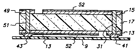
Figure 5 is a plan view of another circuit protection .
device of the invention which has been soldered to a circuit
board, and Figure 6 is a cross section on line VI-VI of Figure
5. The device is similar to that shown in Figures 1 and 2 but
has been made symmetrical so that it can be placed on a circuit
board either way up. Thus the device includes a second cross-
conductor 31 which connects the second electrode 15 to a second
additional member 35. The cross-conductors were made by plating
the apertures (and the other exposed surfaces) first with copper
and then with solder. The device has been soldered to traces 41
and 43 on an insulating substrate 9. During the soldering
process the solder plating on the device flows and completely
fills the apertures.
- Figure 7 is a plan view of a part of an assembly of the
invention which can be divided into a number of individual
devices as shown in Figures 1 and 2, and Figure 8 is a cross
section on line VIII-VIII of Figure 7. The assembly includes a
laminar PTC element 7 having a first face to which first laminar
conductive member 3 is attached and a second face to which
second laminar conductive member 5 is attached. The conductive
members 3 and 5 are not continuous but are in the form of
parallel strips formed by removing, e.g. by etching, strips of
electrode material from a corresponding continuous member. The
material is removed in staggered strips alternately from
opposite sides of the assembly, in order to balance the physical
stresses in the product. Before the etching step, a plurality
WO 95/08176 21717 4 9 pCT~S94/10137
-17-
of holes, arranged in a regular pattern, have been drilled
through the PTC element 7 and the laminar members 3 and 5, and
the assembly has then been plated to provide a tubular cross-
conductor 1 in each of the apertures (and a plating 2 on other
exposed surfaces of the assembly). The assembly can be
converted into a plurality of devices by dividing it along the
lines marked C. At the edge of the assembly, there are
registration holes 4 for use in locating the holes to be drilled
through the element 7 and members 3 and 5, and in locating the
lines of division C.
The invention is illustrated by the following Example.
A conductive polymer composition was prepared by pre
blending 48.6 by weight high density polyethylene (PetrotheneTM
LB 832, available from USI) with 51.4 by weight carbon black
(RavenTM 430, available from Columbian Chemicals), mixing the
blend in a BanburyTM mixer, extruding the mixed compound into
pellets, and extruding the pellets though a 3.8 cm (1.5 inch)
extruder to produce a sheet with a thickness of 0.25 mm (0.010
inch). The extruded sheet was cut into 0.31 x 0.41 meter (12 x
16 inches) pieces and each piece was stacked between two sheets
of 0.025 mm (0.001 inch) thick electrodeposited nickel foil
(available from Fukuda). The layers were laminated under heat
and pressure to form a plaque with a thickness of about 0.25 mm
(0.010 inch)-. Each plaque was irradiated to 10 Mrad. Each
plaque was used to prepare approximately 7000 devices, each
having the configuration shown in Figures 1 and 2.
Holes with a diameter of 0.25 mm (0.010 inch) were drilled _
through the thickness of the plaque in a regular pattern to
provide~one hole for each device. Each hole was deburred and
cleaned. The surface of both the nickel foil layers and the
conductive polymer surrounding the drilled hole were sensitized
using a palladium/copper solution. A copper layer approximately
0.076 mm (0.003 inch) thick was electroless plated onto the
sensitized surfaces and then a 0.025 mm (0.001 inch) thick layer
WO 95/08176 PCT/US94110137
-18-
of tin-lead solder was electroless plated onto the copper
surface. Using the following standard photoresist process, a
pattern was etched onto the plaque. First, a dry film (MylarT~'
polyester) resist was laminated onto both surfaces of the plaque
and then exposed to ultraviolet light to generate a pattern as
shown in Figures 7 and 8. Second, a ferric chloride solution
was used to chemically etch the pattern. During this step,
alternating sections on each side of the plaque were etched away
to expose the solder and relieve built-up mechanical stress.
Third, the etched plaque was rinsed and the resist was stripped
away.
The plaque was sheared and diced to produce individual
rectangular electrical devices. Each device had dimensions of
4.57 x 3.05 x 0.51 mm (0.180 x 0.120 x 0.020 inch). The
through-hole was positioned approximately 3.81 mm (0.015 inch)
from the shorter edge of the device. A strip of exposed
conductive polymer 0.51 x 3.05 mm (0.020 x 0.120 inch) was
present 0.38 mm (0.015 inch) from the through-hole and 1.02 mm
(0.040 inch) from the shorter edge of the device. Each device
had a resistance of approximately 300 mohm.