Note: Descriptions are shown in the official language in which they were submitted.
~. '~ 19 ~
OPTICAL IMAGE PROCESSOR EMPLOYING A NONLINEAR MEDIUM
WITH ACTIVE GAIN
Field of the Invention
The invention relates to optical image processors of the kind in
which image information is stored in a nonlinear medium that imparts gain.
6 Art Background
It has long been recognized that optical image processors can
perform a wide variety of optical processes. For example, image correlators
are
a type of image processor which can be used for pattern recognition. One class
of
image correlators are known as "joint Fourier transform optical correlators."
In
these devices, conveniently described with reference to FIG. 1, Fourier-
transform
12 lens 80 operates on a pair of coherent images representing a reference R
and an
unknown object S. The resulting optical intensity distribution in the focal
plane
of the Fourier-transform lens is recorded in a nonlinear medium 25 that
typically
comprises a photorefractive material. The output of the correlator is
generated
by a Fourier-transform lens (also shown in the figure as lens 80) operating on
the
recorded pattern. Each of two side regions of the output image (symmetrically
18 displaced from the center by the separation between R and S) contains an
intensity distribution corresponding to the cross correlation between R and S.
The position of a correlation peak identifies the location of a feature of R
that
resembles S. The height of the peak measures the degree of similarity. A
correlator of this kind is described, e.g., in H. Rajbenbach et al., "Compact
photorefractive correlator for robotic applications," Abp-Opt. 31 (1992) 5666-
24 5674. This system used a crystal of Bil2 Si020 (BSO) as the photorefractive
medium. With this material, a typical response time of about 50 ms was
achieved. Using a crystal about 1 mm thick, diffraction efficiencies of 0.1 % -
1
were obtained.
CA 02171996 1999-03-30
2
A second class of correlators are known as "Vanderlugt optical 25
correlators." These devices are described, e.g., in D.T.H. Liu et al., "Real-
time Vanderlugt
optical correlator that uses photorefractive GaAs," Appl. Optics 31 (1992)
5675-5680. In
these correlators, conveniently described with reference to FIG. 2, the
Fourier transform
of, e.g., the S image is written in nonlinear medium 25 by interfering it with
reference
beam 5, which is typically a plane wave. The output of the correlator is
generated by using
lens 84 to create a Fourier transform of the R image, which is impinged on the
photorefractive medium. As depicted in the figure, lens 82 is used both to
generate the
Fourier transform of the S image, and to generate the inverse Fourier
transform of the
output from the nonlinear medium.
The system described by D. T. H. Liu et al. used a crystal of gallium
arsenide, 5 mm thick, as the photorefractive medium. Diffraction efficiencies
less than
0.1 % were obtained. The shortest response time measured was 0.8 ms at a laser
intensity
of about 1.5 W/cm2.
U.S. Patent No. 5,606,457 issued February 25, 1997 to T.H. Chiu, discloses
an optical image correlator that uses the nonlinear optical properties of semi-
insulating,
multiple quantum well (SI-MQW) structures. This system can perform correlation
operations in 1 ps or less with diffraction efficiencies as great as 3% or
less.
One limitation of known optical image processors such as those described
above is that the nonlinear materials they employ are passive structures that
absorb
significant amounts of optical energy. As a result, the output from the image
processor is
often as much as two orders of magnitude smaller than the magnitude of the
input signal.
More efficient photorefractive materials may be employed to reduce the optical
absorption, but at the expense of a decreased response time.
Accordingly, it is desirable to provide an optical image processor that has a
rapid response time so that great volumes of data can be processed while at
the same time
imparting gain to the input signal rather than a loss.
Summary of the Invention
The invention relates to an optical image processor of the kind that includes
an input source and an output source of coherent light. (The term "light" is
meant to
CA 02171996 1999-03-30
include invisible portions of the electromagnetic spectrum, such as infrared
radiation.) The
input source provides input beams of light that may include a control beam and
a signal
beam. The processor further includes means for impressing on the input light
spatial
intensity modulation patterns corresponding to at least one input image, a
lens for creating
a Fourier transform of the modulation pattern, and a nonlinear medium for
recording the
Fourier transform as an absorption-modulation and/or refractive modulation
pattern, and
for modulating the output light in accordance with the recorded pattern. In
contrast to
processors of the prior art, the nonlinear medium of the inventive processor
includes an
active gain medium such as a vertical-cavity surface-emitting laser or an
optically pumped
gain medium. By using an active medium the resulting processor provides an
output that
exhibits less loss in power than the known processors without a significant
sacrifice in
response time. As a result, a plurality of such processes may be cascaded
together without
concern for power degradation. Moreover, the process may be employed to
perform a
variety of processing functions by feeding back the optical signal through the
gain medium
a plurality of times from different spatial locations.
In accordance with one aspect of the present invention there is provided an
optical image processor, comprising: a) first and second coherent input beams
of light; b)
means for impressing on the first input beam a coherent spatial, intensity-
modulation
pattern corresponding to at least a first input image; c) a lens for creating
a Fourier
transform of the modulation pattern; d) a third input beam having impressed
thereon a
coherent modulation pattern corresponding to at least a second input image;
and e) a
nonlinear medium for coherent processing by a four-wave mixing process, (i)
the
modulation pattern created from the Fourier transform, (ii) said second input
beam and
(iii) the second input image, to generate a modulated output beam, said
nonlinear medium
including an active gain medium operable to impart gain, by at least one of
optical
pumping and electrical injection, to the first input beam having an intensity
modulation
pattern impressed thereon.
Brief Description of the Drawings
FIG. 1 is a schematic, block diagram of a joint Fourier transform optical
image correlator.
CA 02171996 1999-03-30
4
FIG. 2 is a schematic, block diagram of a Vanderlugt optical image
correlator.
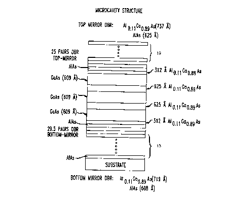
FIG. 3 shows an example of a VCSEL structure that may serve as the active
gain medium in the image processor of the present invention.
Detailed Description
The inventive processor will be described as either a joint Fourier transform
correlator or a Vanderlugt correlator. In either case, the general features of
the processor
are well known. A joint Fourier transform correlator is described, e.g., in H.
Rajbenbach
et al., cited above. A Vanderlugt correlator is described, e.g., in D.T.H. Liu
et al., cited
above. By way of illustration, we now briefly describe, with reference to FIG.
1, a joint
Fourier transform correlator that we have used successfully in experimental
trials.
Modifications of this system to achieve, instead, a Vanderlugt correlator will
be readily
apparent to the skilled practitioner.
A beam of input light is provided by laser 10, which is exemplary a
vertically polarized, 150 mW, single longitudinal mode diode laser emitting at
830 nm. A
beam of output light is provided by laser 20, which is exemplary a vertically
polarized,
single longitudinal mode diode laser emitting at 850 nm. Laser 20 is typically
operated at a
power level of about 10 mW. Its emission wavelength can be temperature-tuned
to
maximize the diffraction efficiency from photorefractive medium 25. The beam
from each
of lasers 10 and 20 is passed through an optical subsystem 30, 40 consisting
of a lens, an
anamorphic prism pair, and a beam expander. These subsystems expand and
collimate the
laser beams.
Modulator 50 is exemplary a liquid-crystal, spatial light modulator such as
sold by the Epson corporation as the Epson Crystal Image Video Projector
(trade mark).
This modulator has an aperture of 2.0 cm x 2.6 cm, and a pixel resolution of
320 x 220.
This modulator, as purchased, includes polarizer films that are removed before
the
modulator is incorporated in the correlator. The modulator is driven with a
video signal
from video source 60 to produce a control beam and a signal beam which in the
particular
case of a correlator correspond to a pair of side-by-side images R and S,
respectively. (At
this stage, the images are not visible because they exist only as a
polarization rotation.)
~~'~l~~u
Polarizing beam-splitter cube 70 converts the pattern of polarization rotation
to a
pattern of intensity modulation.
Lens 80, exemplary a doublet lens with a focal length of 26 cm,
operates on the input beam to produce a Fourier transform of the input images.
More precisely stated, nonlinear medium 25, situated at the Fourier plane of
lens
80, records the interference pattern corresponding to the multiplicative
product
of the Fourier transforms of the respective input images.
The output beam reads the recorded pattern by passing through
the nonlinear medium. The output beam then passes through lens 80, with the
result that the inverse Fourier transform of the recorded pattern is carried
by the
output beam. The output beam then falls on CCD camera 100 situated at the
12 back focal plane of lens 80. The output of camera 100 is recorded by frame
grabber 105. To remove spurious light at 830 nm (i.e., the wavelength of the
input beam), a band-pass interference filter 110 centered at 850 nm (i.e., the
wavelength of the output beam) is placed between lens 80 and camera 100. To
reduce the optical intensity impinging on camera 100, a neutral density filter
120
(typically with a density of 1) is also placed between the lens and the camera
A
t s beam block 130 situated between the lens and the camera excludes that
component of the output beam having zero spatial frequency.
In contrast to processors of the prior art, nonlinear medium 25 of
the inventive correlator is an optically pumped semiconductor material that
imparts gain to an input beam. Devices of this kind that may be employed in
the
present invention are described generally in Y. Yamamoto et al., Coherence,
24 Amplification and Quantum Efficiency in Semiconductor Lasers, Ch.13,1991,
John Wiley & Sons, Inc. While prior art processors employ photorefractive
materials to achieve nonlinear results, the inventive processor takes
advantage of
the nonlinear properties that are inherent in semiconductor materials. One
class
of optically pumped semiconductor materials that may be employed is a vertical-
cavity surface-emitting laser (VCSEL) structure operating below its lasing
CA 02171996 1999-03-30
6
threshold. A VCSEL is composed of an active gain material such as a
GaAs/AIGaAs
multilayer structure which is disposed between mirrors that form a Fabry-Perot
cavity.
These structures can produce gain by electrical injection. The cavity
increases the
efficiency of the device by providing feedback to the input signal so that the
total gain is
increased over that imparted by the active gain material itself. The nonlinear
nature of a
VCSEL device has been used to demonstrate four-wave mixing in Jiang et al.,
Conference on Lasers and Electrooptics, vol. 8, pp. 224-225, 1984, OSA
Technical
Digest Series, Optical Society of America. However, this reference does not
show the
use of a VCSEL structure in an optical image processor.
By way of illustration, we now briefly describe a VCSEL device that may
be used in the inventive processor. This device is more fully described in
U.S. Patent
No. 5,513,203 entitled Surface Emitting Laser Having Improved Pumping
Efficiency.
FIG. 3 shows a VCSEL structure designed to operate at a wavelength of 870 nm.
The
top mirror 19 is formed from 25 pairs of alternating layers of Alo.,~Gao.89As
(737 ~) and
AIAs (625 A) and the bottom mirror is formed from 29.5 pairs of Alo."Gao.89As
(719 ~)
and AIAs (608 A). The gain medium is formed from three active layers of GaAs
(609 ~) each separated by barrier layers of Alo "Gao g9As (625 ~). A barrier
layer of
Alo."Gao.g9As (312 t~) is interposed between the active layers and each of the
mirrors 13
and 19. The active layers are located at the antinodes of the standing wave
supported
between the mirrors 13 and 19 to maximize efficiency. The high reflectivity
bandwidth
of the bottom mirror 13 is shifted by approximately 14 nm relative to the top
mirror 19.
The mirrors 13 and 19 are also "unbalanced," as this term is defined in U.S.
Patent
No. 4,999,842, for example. That is, the bottom mirror 13 employs a greater
number
of alternating layers than the top mirror 19. As a result, the reflectivity of
the bottom
mirror 13 is greater than the reflectivity of the top mirror 19 at the
~1'~~.~~~
design wavelength. The optical output beam will be emitted from the top mirror
19 because of its decreased reflectivity relative to the bottom mirror 13.
It should be noted in this regard that the semiconductor material
is not necessarily based on a III-V material system. For example, II-VI
materials
may also be employed as the active gain material.