Note: Descriptions are shown in the official language in which they were submitted.
21~568
VOLTAGE COMPARATOR REQUIRING NO COMPENSATING OFFSET VOLTAGE
Technical Field of the Invention
The present invention relates generally to voltage comparators and more particularly to a
voltage comparator that does not require a compensating offset voltage.
S PL~ kground of the Invention
Known analog voltage comparators are often constructed using a differential pair of
transistors in which the voltages to be compared are each supplied to a different input transistor.
One limitation of this configuration is that there is an inherent offset error due to the unavoidable
deviation in the characteristics of different transistors (i.e., transistor mismatch). This offset
10 error often amounts to about 10 mV, which is too large for many applications. For example, if
one volt represents 8 bits of data yielding 256 distinct states, only about 4 mV separates adjacent
states. Clearly an error greater than 4 mV is often intolerable.
Comparators are known which compensate for the offset error by providing a
compensating voltage, but these comparators require additional circuitry and hence are unduly
15 complex. Examples of such comparators are shown in E.A. Vittoz, "Dynamic Analog
Techniques," VLSI Circuits for Telecommunications, edited by Y.P. Tsividis and P. Antognetti,
Prentice Hall, 1995.
Summary of the Invention
The present invention provides a method and apparatus for comparing a first input
20 voltage to a second input voltage. The invention overcomes the problem of transistor mismatch
without the need for a compensating offset voltage and thus without the need for additional
2 21725~8
circuitry. The invention achieves this result by applying the first and second input voltages to
the same input transistor rather than to two different transistors. As a result, the two voltages
undergoing comparison experience the same environment and consequently the problem of
transistor mismatch does not arise.
In accordance with the method of the invention, a first input voltage is transformed into a
first current flowing through a first transistor and a second transistor. A second input voltage is
transformed into a second current flowing through the first transistor while the first current
continues flowing through the second transistor. A difference current is developed which
represents the difference between the first current and the second current. An indicator signal is
generated which indicates the larger of the first and second input voltages based on the value of
the difference current.
In one particular embodiment of the invention, the apparatus includes a first transistor of
a first polarity. The first transistor has a drain-source path, a gate for selectively receiving the
first and second input voltages, and a first source terminal for receiving a first supply voltage. A
switching element is provided for selectively applying the first and second input voltages to the
gate of the first transistor. A second transistor of a polarity opposite to the first polarity is also
provided. The second transistor has a drain-source path serially coupled to the drain-source path
of the first transistor and a second source terminal for receiving a second supply voltage. An
output terminal is coupled to the drains of the first and second transistors. A switch is provided
for selectively coupling the gate of the second transistor to the output terminal.
In one alternative embodiment of the invention, the first input voltage, offset by an offset
voltage, is stored as a stored voltage. A differential voltage is developed between the second
input voltage, also offset by the offset voltage, and the stored voltage. An output signal
3 ~172~6B
proportional to the differential voltage is generated. The output signal indicates the larger of the
first and second input voltages. In one embodiment of the invention, these steps are performed
with an apparatus that includes an operational amplifier having an inverting input, a non-
inverting input, and an output. A switching element selectively applies the first and second input
voltages to the noninverting input of the operational amplifier. A capacitor has a first terminal
coupled to the inverting input of the operational amplifier and a second terminal for receiving a
supply voltage. A switch selectively couples the output of the operational amplifier to the
inverting input of the operational amplifier.
In another alternative embodiment of the invention, the first input voltage, offset by an
offset voltage, is stored as a stored voltage. The second input voltage is also offset by the offset
voltage to form an offsetting second voltage. An output signal is generated which represents a
difference between the stored voltage and the offsetting second voltage. The output signal
indicates the larger of the first and second input voltages.
Brief Description of the Drawin~
FIG. I shows a voltage comparator constructed in accordance with the present invention.
FIG. 2 shows an alternative embodiment of the voltage comparator which employs asource follower to provide immunization from noise.
FIG. 3 shows another alternative embodiment of the invention in which a plurality of the
voltage comparators shown in FIG. I are cascaded together to increase gain.
FIG. 4 shows yet another alternative embodiment of the invention which employs an
operational amplifier.
4 ~i7~S68
Detailed Description
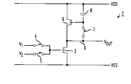
FIG. I shows an exemplary voltage comparator 2 constructed in accordance with one
embodiment of the present invention. The input voltages Vl and V2 that are to be compared are
selectively coupled to the gate of a first MOS transistor 3 via switches 4 and 5, respectively.
5 That is, the input voltages V~ and V2 may be sequentially directed to the gate of the first
transistor 3 by alternately closing and opening the switches 4 and 5. The first MOS transistor 3
has its source terminal connected to a first voltage supply Vss that is, for example, at ground
potential. The drain of the first transistor 3 is coupled to the drain of a second MOS transistor 6.
The source of the second MOS transistor 6 is connected to a second voltage supply VDD that is
10 maintained at a higher potential than the first voltage supply Vss. The output terrninal 9 of the
voltage comparator 2 is connected to a node located intermediate to the drains of the first and
second transistors 3 and 6. The gate of the second MOS transistor 6 is selectively coupled to the
output terminal 9 via a switch 7. As one of ordinary skill in the art will recognize, when switch 7
is closed, the second MOS transistor is in a diode mounted configuration. The gate of the second
15 MOS transistor 6 also may be optionally connected to a capacitor 8 that is in turn connected to a
constant reference voltage such as the second voltage supply VDD, for example. The capacitor 8
may be advantageously employed when the parasitic or inherent gate-source capacitance of the
second MOS transistor 6 is insufficient to m~int~in the voltage at the gate of the second
transistor 6. The capacitor 8 may be a charge storage device such as a conventional capacitor or
20 a MOS transistor in which the capacitance arises between the gate and transistor substrate.
The first and second MOS transistors 3 and 6 should have opposite polarities. Thus, in
the exemplary embodiment of the invention shown in FIG. 1, the first MOS transistor 3 is an n-
MOS transistor and the second MOS transistor 6 is a p-MOS transistor. Alternatively, the first
5 ~i72~68
MOS transistor 3 may be a p-MOS transistor and the second MOS transistor 6 may be an n-MOS
transistor. In this latter case the first voltage supply Vss should be at a higher potential than the
second voltage supply VDD
In operation, the switches 4, 5, and 7 are initially in their open state. Switches 4 and 7
5 are then closed, applying the first input voltage Vl to the gate of the first transistor 3. In a MOS
transistor, the drain-source current Ids depends on the applied gate-source voltage Vgs Thus, the
input voltage Vl is in effect transformed into a current Ids(VI) that flows through the source-drain
path of the first transistor 3. Since the first and second transistors 3 and 6 are serially connected,
the current Ids(VI) flowing through the first transistor 3 also flows through the second transistor
10 6. The current Ids(V,) flowing through the second transistor 6 causes a voltage Vgs to appear
between the gate and source of the second transistor 6 since the second transistor 6 is diode
mounted when switch 7 is closed. This voltage is maintained or stored in the second transistor 6
by the parasitic gate-source capacitance of the transistor, and possibly by the capacitor 8 as well,
if employed. Switch 7 may now be opened and the current Ids(VI) flowing through the second
15 transistor 6 will be maintained by the stored voltage.
In the next operational step, switch 4 is opened and switch 5 is closed so that the second
input voltage V2 is applied to the gate of the first transistor 3. Similar to the step previously
described in which the first input voltage Vl was transformed into a current flowing through the
first transistor 3, the second input voltage V2 now gives rise to a current Ids(V2) flowing through
20 the first transistor 3. Thus, a current Ids(VI) now flows through the second transistor 6 while a
current Ids(V2) flows through the first transistor 3. If the currents Ids(VI) and Ids(V2) are not
identical, a difference current will be generated at the output terminal 9 of the comparator 2. The
difference current will bring the unloaded output of the comparator 2 into saturation. That is, the
- 6 ~172568
comparator output terminal 9 will provide a voltage equal to one of the supply voltages Vss or
VDD when the currents Ids(V,) and Ids(V2) are unequal. More particularly, if the current Ids(VI)
is greater than the current Ids(V2) the comparator output terminal 9 will be at a voltage VDD. If
the current Ids(VI) is less than the current Ids(V2), the comparator output terminal 9 will be at a
S voltage Vss. Thus, the voltage appearing at the comparator output temminal 9 indicates whether
the first input voltage Vl is greater or less than the second input voltage V2.
In summary, the comparator undergoes two distinct periods during its operation. In a
first period denoted a transfer period, the first input voltage is applied to the comparator,
transferred to the second transistor 6 and stored in a capacitor. In a subsequent period denoted a
10 compare period, the second input voltage is applied to the comparator and the comparator
generates an output voltage indicating the larger of the first and second input voltages.
The comparator 2 may be operated in a variety of modes. In one mode an input voltage,
say the first input voltage Vl, has a constant value over time. In this mode the second input
voltage may be continuously applied to the comparator by leaving switch S in its closed state
15 after the constant input voltage Vl has been transferred to the second transistor 6 by first closing
and then reopening switches 4 and 7. In this manner the comparator remains in its compare
period so that the second input voltage V2 is continuously compared to the constant input voltage
Vl.
In a second mode of operation the input voltages are variable. In this mode the switches
20 4 and 7, operated in unison, must be altemately opened and closed with switch 5 each time a
comparison is to be perfommed so that the comparator 2 alternates between its transfer and
compare periods. As a result, new values of the input voltages Vl and V2 will be input and
compared after the completion of each compare period. The first mode of operation is
7 ~17~56~
advantageously employed whenever only one of the input voltages is variable because the
dynamic power requirements are less in this mode of operation and because continual switching
generates noise.
FIG. 2 shows an alternative embodiment of the invention similar to that shown in FIG. I
except that a source follower comprising serially connected transistors 40 and 41 is inserted
between the gate of the first transistor 43 and the switches 44 and 45. The source follower is
used to reduce noise from the first voltage supply Vss, which may occur whenever current is
injected into a supply rail with non-zero resistivity. This noise reduction is achieved by applying
to the gate of transistor 40 a reference voltage Vref that is immune to noise. The reference
voltage Vref may be more readily immunized from noise than the voltage supply Vss because,
unlike Vss, the reference voltage Vref only supplies a voltage and does not draw current.
As seen in FIG. 2, the source of transistor 40 is connected to the first supply voltage Vss
and the drain of the transistor 41 is connected to the second supply voltage VDD. The drain of the
transistor 40 is connected to the source of transistor 41. A reference voltage is supplied to the
gate of the transistor 40 and the input voltages Vl and V2 undergoing comparison are selectively
input to the gate of the transistor 41 via switches 44 and 45, respectively. The transistors 40 and
41 should be of the same dimensions so that they have the same operational characteristics. The
gate of the first transistor 43 is connected to a node located between the drain of transistor 40 and
the source of transistor 41.
The following discussion will explain how the comparator shown in FIG. 2 is
immunized from noise by the source follower. The voltage at the gate of the first transistor 43 is
equal to Vjn - (Vref - Vss), where Vjn is equal to either V~ or V2, depending on whether switch 44
or switch 45 is closed. The voltage at the source of the first transistor 43 is equal to Vss.
8 217256~
Accordingly, the voltage VgS43 between the gate and source of the first transistor 43 is equal to
Vin - Vref and thus the input voltage to the first transistor 43 is independent of the supply voltage
Vss~
The reference voltage should be selected so that it is equal to or greater than the
5 threshold voltage of the transistor 40 so that the transistor 40 remains on. However, as explained
below, when the reference voltage increases the range of voltages that may be compared by the
comparator decreases. Therefore, a reference voltage should be selected that is not much larger
than the threshold voltage to m~ximi7e the input dynamic range (i.e., the lower bound of the
voltage Vjn) of the comparator. The analysis presented below will explain why the input
10 dynamic range decreases as the reference voltage increases.
An examination of FIG. 2 leads to the following equality:
Vjn - VSS = VGS41 + VGS43 (I)
where VGS41 and VGS43 are the gate-source voltages of transistors 41 and 43, respectively, and the
remaining voltages have been previously defined. The gate-source voltage of transistor 43 must
15 be larger than the threshold voltage so that the transistor does not turn off. That is,
VGS43 > Vth (2)
Equation (1) thus becomes
Vjn - VSS ~ VGS41 + Vth (3)
The gate source voltage of transistor 40 is
VGS40 = Vref - VSS (4)
Since transistors 40 and 41 have the same sizing
VGS40=VGS41
Rewriting equation (3) using equations (4) and (5) to eliminate VGS41 results in
~17256~
Vin > Vref +Vth (6)
Equation (6) shows that the lowest acceptable value for the input voltages Vl and V2 for the
comparator shown in FIG. 2 is Vref + Vth. Therefore, as previously noted, the reference voltage
Vref should be minimized to maximize the input dynamic range.
In practice of course, the comparator output is loaded and as a result the output voltage
will not reach either VDD or Vss when the difference current representing the difference between
Ids(V2) and Ids(VI) is small. Thus, in order to increase the gain and as a consequence the
sensitivity of the comparator a cascaded structure such as shown in FIG. 3 may be used. While
FIG. 3 shows a two-stage comparator in which two of the FIG. 1 comparators are cascaded
together, one of ordinary skill in the art will recognize that in general an N-stage comparator may
be used, where N is any desired number of individual comparators which are cascaded together.
The comparators shown in FIG. 3 are cascaded together by coupling the output terminal 32 of
the first comparator 30 to the gate of the first transistor 34 in the second comparator 31. The
cascaded comparator operates in the same manner as the single stage comparator shown in FIG.
1 except that the switches 35 and 36 respectively connecting the gates of the second transistors in
the first and second comparators 30 and 31 to the output terminals 32 and 37 must both be
operated in synchronism. The gain of the N-stage comparator equals Al A2 A3, ..., AN~ where Ak
is the voltage gain of stage k. The voltage gain Ak of stage k is defined as the voltage change
that appears at the output of stage k for a given voltage change appearing at the input of stage k
20 (i.e., at the gate of the first transistor in stage k).
FIG. 4 shows an alternative embodiment of the invention which employs an operational
amplifier 20. Operational amplifiers are well known devices that provide high open loop gain,
high input impedance and low output impedance. Additional details concerning the
lo 2172~68
characteristics and structure of operational amplifiers are not a part of this invention and hence
will not be discussed further.
As seen in FIG. 4, the operational amplifier is coupled to supply voltages Vss and VDD.
In contrast to the previous embodiments of the invention, the output of the operational amplifier
can swing between almost completely between Vss and VDD. The input voltages Vl and V2 are
selectively applied to the noninverting input terminal 21 of the operational amplifier 20 via
switches 22 and 23, respectively. The inverting input terminal 24 of the operational amplifier 20
is connected to a capacitor 25. The capacitor 25 may be a charge storage device such as a
conventional capacitor or a MOS transistor in which the capacitance arises between the gate and
transistor substrate. The capacitor 25 is in turn connected to a constant voltage source, which as
illustrated in FIG. 4, may be at ground potential. The inverting input terrninal 24 of the
operational amplifier 20 is also selectively connectable to the output 26 of the operational
amplifier 20 via a switch 27. The output 26 of the operational amplifier 20 serves as the output
of the voltage comparator.
The operation of the comparator shown in FIG. 4 is similar to that of the comparator
shown in FIG. 1. That is, the comparator shown in FIG. 4 undergoes both a transfer period and a
compare period during its operation. In the transfer period, switches 22 and 27 are both closed.
As one of ordinary skill will recognize, the output voltage VOUt ~ppeafing at the output terminal
26 of an operational amplifier may be expressed as follows:
VOut= A(V+ - V + Voff) (7)
where A is an appropriate proportionality constant, V+ is the voltage at the noninverting input, V
is the voltage at the inverting input, and Vof~ is an offset voltage inherent in the operational
amplifier due to the mismatch between the input transistors.
11 ~ 1 72568
When switches 22 and 27 are closed so that V+=VI and V =VOU', this equation reduces
to:
V = [A/(A+I)] (Vl + Voff) (8)
Since A is infinite for an ideal operational amplifier, this equation can be approximated as:
V = Vl +Voff (9)
As equation (9) indicates, when switches 22 and 27 are both closed the voltage at the inverting
input terminal 24 equals the first input voltage Vl offset by the voltage Voff. This voltage at the
inverting input will appear across the capacitor 25. In the second part of the transfer period
switch 27 is opened so that the voltage Vl + Voff is stored across the capacitor 25.
In the compare period of operation switch 22 is opened and switch 23 is closed so that
the second input voltage V2 appears at the noninverting input terminal V+. Substituting into
equation 7 the voltages presently appearing at the positive and negative input terminals yields:
Vout = A(V2 - (V, +Voff) + Voff) = A(V2-V,) (10)
Accordingly, the output voltage VOut is independent of the offset voltage Voff and the
15 sign of the output voltage Vout indicates the larger of the two input voltages. More particularly,
as with the first embodiment of the invention, the output voltage VOut will equal one of the
supply voltages Vss or VDD supplied to the operational amplifier depending on whether Vl or V2
is the larger voltage. An N-stage comparator may be formed by cascading together two or more
of the single stage comparators shown in FIG. 4 in the same manner shown in FIG. 3. That is,
20 the output of each operational amplifier is coupled to the noninverting input of the succeeding
operational amplifier.
The embodiments of the invention shown in FIGS. 1-3 may be fabricated from discrete
MOS transistors. Alternatively, these embodiments may be fabricated as a monolithic device
12 217~68
using a conventional digital Complementary Metal Oxide Semiconductor (CMOS) process. The
embodiment of the invention shown in FIG. 4 employing an operational amplifier may be
fabricated by any conventional process, including bipolar or CMOS processes, or a combination
thereof.