Note: Descriptions are shown in the official language in which they were submitted.
CA 02173034 1998-12-11
-1-
BiMOS INTEGRATED CIRCUIT
FIELD OF THE INVENTION
This invention relates to a BiMOS (Bipolar Metal-Oxide-
Semiconductor) integrated circuit, and more particularly to, a
BiMOS integrated circuit in which a bipolar transistor and a MOS
transistor are integrated on a common semiconductor substrate.
BACKGROUND OF THE INVENTION
Fig. 1 shows a conventional BiNMOS (Bipolar n-channel Metal-
Oxide-Semiconductor) inverter. It comprises a first NPN transis-
for 29 in which the collector is connected to a high potential
power source (hereinafter referred to as Vcc) 1 and the emitter
is connected to an output terminal 8, NMOS (n-channel Metal-
Oxide-Semiconductor) 30 in which the source, drain and gate are
connected to GND 2, output terminal 8 and input terminal 7, res-
pectively, PMOS (p-channel Metal-Oxide-Semiconductor) 31 in which
the source, drain and gate are connected to Vcc 1, the base of
the NPN transistor 29 and input terminal 7, respectively, and
NMOS 32 in which the source, drain and gate are connected to GND
2, the base of the NPN transistor 29 and input terminal 7,
respectively.
Herein, the gate width of NMOS 30 is set at that required
to pull down a given load capacitance at a sufficient speed. For
example, the gate width is 10 ~,m. The gate width of PMOS 31 is
set to sufficiently shorten the time to charge the base of the
NPN transistor 29. For example, the gate width is 12 ~cm. The
gate width of NMOS 32 is set to sufficiently fast pull down the
parasitic capacitance around the base of the NPN transistor 29.
For example, the gate width is 5 ~,m.
CA 02173034 1998-12-11
-2-
In operation, when the potential of the input terminal 7 is
changed high to low, PMOS 31 turns on and NMOS 32 simultaneously
turns off thereby turning on the NPN transistor 29 to charge a
load capacitance. Here, NMOS 30 turns off thereby not flowing
a penetrating current between the NPN transistor 29 and NMOS 30.
When the potential of the input terminal 7 is changed low
to high, PMOS 31 turns off and NMOS 32 simultaneously turns on
thereby cutting off the base current for the NPN transistor 29
to reduce the base potential. Here, NMOS 30 turns on thereby
discharging the load capacitance to get down the output poten-
tial. If the gate width of NMOS 32 is set such that the falling
speed of the base potential of the NPN transistor 29 is faster
than that of the potential of the output terminal, the NPN tran-
sistor 29 continues to turn off to stop the penetrating current.
The power consumed in the above operation is mainly a power
for the charge-and-discharge of the gate capacitance of MOS
transistor and source and drain diffusion capacitance.
Fig. 2 shows a conventional CMOS (Complementary Metal-Oxide-
Semiconductor) inverter. PMOS 9 is used for pulling up the out-
put potential and NMOS 10 is used for pulling down the output
potential.
It is known that the gate width ratio of PMOS 9 and NMOS 10
is set about 2:1 to obtain the highest speed since ON current per
unit gate width of PMOS is about 1/2 that of NMOS. Furthermore,
the rise and fall time of the output potential can be balanced.
For example, the gate widths of PMOS 9 and NMOS 10 are set 20 and
to ~cm, respectively.
According as the gate width of PMOS 9 is reduced, the rise
time of the output becomes longer. However, since the logical
2 ~ 73034
-3-
threshold is simultaneously reduced, the operating speed in the
case of connecting a gate with the same circuit constant is not
highly degraded. Thus, in a gate array etc., to give priority
to the integration density and consumed power, the gate width
ratio of PMOS and NMOS 10 may be reduced to about 1.2:1. In this
case, the gate widths of PMOS 9 and NMOS 10 are, for example, set
12 and 10 um, respectively.
However, it is not preferable that the ratio is less than
1:1. Because, in the case that a constant total gate width is
set, if a larger gate width is assigned to NMOS therefrom, the
consumed power is not reduced and the operating speed is
decreased.
The operation speeds of the above-mentioned CMOS gate
circuit and BiNMOS gate circuit are generally equal under a low
load condition. Therefore, when a circuit block with a complex
logic is composed, the main section is generally composed of the
CMOS gate circuit which facilitates to compose the circuit and
has a high integration density and BiNMOS is used only for the
output section and a section with a large fan-out.
The above logical circuits can be composed as a master-slice
type semiconductor integrated circuit in which arrays of
transistors, resistance elements etc. are previously placed on
a semiconductor substrate and the elements on the substrate are
interconnected on the wiring process.
FIG.3 shows a basic cell layout for a conventional BiNMOS
gate array. Two PMOSs 34 and 35 are formed on a common diffusion
region 33 and have commonly a diffusion region contact.
Similarly, two NMOSs 37 and 38 are formed on a common diffusion
2173034
-4-
region 36 and have commonly a diffusion region contact. Also,
two small NMOSs 40 and 41 are formed on a diffusion region 39
separated from NMOSs 37 and 38, and a NPN transistor 42 is
provided.
The gate widths of PMOSs 34, 35, NMOSs 37, 38 and small
NMOSs 40, 41 are set 12 ~Zm, 10 pm and 5 pm, respectively.
For example, in the BiNMOS inverter in FIG.1, NPN 42 is used
as the NPN transistor 29, PMOS 34 or 35 is used as PMOS 31, NMOS
37 or 38 is used as NMOS 30 for output pull-down, and NMOS 40 or
41 is used as NMOS 32.
In a further complex logical block, a BiNMOS gate is used
in an output drive section and a CMOS gate is used in a logical
composition section. Thus, NMOS 30 for output pull-down of the
BiNMOS gate and NMOS used in the logical composition section have
the same gate width since they use NMOSs 37 and 38 in FIG.3.
Also, PMOS 31 for driving the base of the NPN transistor 29
of the BiNMOS gate and PMOS used in the logical composition
section have the same gate width since they use PMOSs 34 and 35.
FIG.4 shows a basic cell layout for a conventional CMOS gate
array. Two PMOSs 44 and 45 are formed on a common diffusion
region 43 and have commonly a diffusion region contact.
Similarly, two NMOSs 47 and 48 are formed on a common diffusion
region 46 and have commonly a diffusion region contact. The gate
widths of PMOSs 44, 45 and NMOSs 47, 48 are set 12 um and 10 ~Zm,
respectively.
FIG.5 shows another example of a basic cell layout for a
conventional BiNMOS gate array which is disclosed in U.S. patent
No. S, 055, 716.
2173034
-5-
In the above example, transistors used only for each of a
CMOS logical section 49 and a BiNMOS buffer section 50 are
provided in the basic cell. Though the CMOS logical section 49
can use MOS transistors with gate widths smaller than that of MOS
transistors used in the BiNMOS buffer section 50, the place where
the BiNMOS buffer is composed must be limited since a NPN
transistor does not exist in the CMOS logical section.
Thus, when small logical blocks such as a BiNMOS inverter
are continuously disposed, or when a gate which has few numbers
of output regardless of many MOS transistors, for example, a 16:1
selector, is placed, useless transistors will be left since the
BiNMOS buffer section is not used so frequently.
As described above, in the conventional BiNMOS logical
integrated circuit, even when the gate width of NMOS for output
pull-down in a BiNMOS gate and the gate width of NMOS in a CMOS
gate are equal, or the gate width of NMOS in the CMOS gate is
shortened by changing the size, the former leads to an increase
in consumed power and a decrease in integration density and the
latter leads to a lack of integration density. As a result, it
can not realize a high integration density and low consumed power
comparing with the same generation CMOS logical integrated
circuit.
SUMMARY OF THE INVENTION
Accordingly, it is an object of the invention to provide a
BiMOS integrated circuit which is provided with a higher
integration density and lower consumed power than the same
generation CMOS integrated circuit.
2 ~ 73034
-6-
According to the invention, a BiMOS integrated circuit,
comprises:
a bipolar transistor for output pull-up;
a BiMOS hybrid gate buffer section which comprises a MOS
transistor for output pull-down which is longitudinally connected
to the bipolar transistor, and a MOS transistor for base drive
which comprises an output which is connected a base of the
bipolar transistor to drive the base and a gate which is
connected to an input; and
a logical section which comprises at least a CMOS gate, the
logical section having an output which is connected to the input;
wherein the base drive MOS transistor has an input
capacitance less than that of the output pull-down MOS
transistor.
Herein, when the wiring length is short in a relatively
small circuit, the wiring capacitance is sufficiently lower than
the capacitance of the gate, source and drain of MOS. Therefore,
even if the gate width of the CMOS gate is decreased and the
input capacitance thereof is less than that of the BiNMOS hybrid
gate, the operating speed is not degraded and the consumed power
can be reduced. The logical section may comprise a CMOS gate and
BiNMOS gate.
The BiMOS integrated circuit of the invention may be
fabricated by a master-slice manner in which a basic cell array
which comprises combining a plurality of transistors is disposed
on a semiconductor substrate and the transistors are
interconnected to implement a given logical function, or by a
master-slice manner in which a basic cell array which comprises
2173034
combining a plurality of transistors is disposed on a
semiconductor substrate and the transistors are interconnected
to implement a given logical function.
To satisfy that " the base drive MOS transistor has an input
capacitance less than that of the output pull-down MOS
transistor" by the master-slice manner or the standard-cell
manner, the output pull-down MOS transistor of the BiMOS hybrid
gate may comprise connecting in parallel MOS transistors which
have the same conductivity type of the logical section, or may
comprise connecting in parallel a MOS transistor which is buried
in an interconnection region and a MOS transistor which has the
same conductivity type of the logical section.
BRIEF DESCRIPTION OF THE DRAWINGS
The invention will be explained in more detail in
conjunction with the appended drawings, wherein:
FIG.1 is a circuit diagram showing a conventional BiNMOS
inverter,
FIG.2 is a circuit diagram showing a conventional CMOS
inverter,
FIG.3 shows an example of a basic cell layout for a
conventional BiNMOS gate array,
FIG.4 shows an example of a basic cell layout for a
conventional CMOS gate array,
FIG S shows another example of a basic cell layout for a
conventional BiNMOS gate array
FIG.6 is a circuit diagram showing a BiNMOS inverter used
for a semiconductor integrated circuit according to the
2173034
_8_
invention,
FIGS.7A and 7B are circuit diagrams showing a three-input
NOR BiNMOS gate and CMOS gate, respectively,
FIG.8 shows a fan-out dependency on a delay time of a BiNMOS
inverter according to the invention,
FIG.9 is a circuit diagram showing a flip-flop used for a
semiconductor integrated circuit according to the invention,
FIG.10 shows a basic cell layout for a gate array in a first
preferred embodiment according to the invention, and
FIG.11 shows a basic cell layout for a gate array in a
second preferred embodiment according to the invention.
DESCRIPTION OF THE PREFERRED EMBODIMENTS
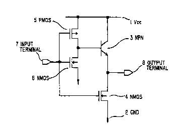
A BiNMOS inverter used for a semiconductor integrated
circuit in the first preferred embodiment will be explained in
FIG.6, wherein like parts are indicated by like reference
numerals as used in FIG.1.
A NPN transistor 3 as an output pull-up device and a NMOS
transistor 4 as an output pull-down device are longitudinally
connected with each other. Namely, the collector terminal of the
NPN transistor 3 is connected to Vcc 1 and the emitter thereof
is connected to an output terminal 8. The source of NMOS 4 is
connected to GND 2 and the drain thereof is connected to the
output terminal 8 and the gate thereof is connected to an input
terminal 7.
In this embodiment, CMOS is used to drive the base of the
NPN 3. Namely, the source of PMOS 5 is connected to Vcc 1 and
the drain thereof is connected to the base of the NPN transistor
- 2173034
-9-
3 and the gate thereof is connected to the input terminal 7. The
source of NMOS 6 is connected to GND 2 and the drain thereof is
connected to the base of NPN transistor 3 and the gate thereof
is connected to the input terminal 7.
The respective transistors have commonly a gate length of
0.5 pm and a gate silicon oxide film thickness of 0.1 pm. The
gate widths are set at, for example, 6 um in PMOS 5, 1.5 pm in
NMOS 6 and 10 ~m in NMOS 4. Namely, the total(7.5 ~Zm) of the
gate widths of PMOS 5 and NMOS 6 for driving the base of the NPN
transistor 3 as an output pull-up device is less than the gate
width(10 Vim) of NMOS 4 as an output pull-down device. Since the
thickness of gate insulating films and channel lengths are common
in the respective transistors, the gate input capacitance of NMOS
4 is greater than the total gate input capacitance of PMOS 5 and
NMOS 6.
In a NAND gate, NOR gate etc. , both the BiNMOS gate in FIG.6
and the CMOS gate in FIG.2 have MOS transistors increased in
proportion to the number of input.
FIGS.7A and 7B are circuit diagrams showing examples of
three-input NOR gates comprising BiNMOS gates and CMOS gates,
respectively. For example, the number ratio of MOS transistors
in the BiNMOS gate as shown in FIG.6 and transistors in the CMOS
gate as shown in FIG.2 is 3:2 in an inverter, 6:4 in a two-input
NAND(NOR) and 9:6 in a three-input NAND(NOR). Thus, the number
ratio of transistors, i.e., the ratio of total gate width is
constant regardless of the logic between the BiNMOS gate and the
CMOS gate. Therefore, the consumed power in the BiNMOS gate is
always less than that in the CMOS gate.
2173034
-10-
FIG.8 shows the fan-out dependency of the delay time of
BiNMOS inverter in a BiMOS integrated circuit of the invention.
The BiNMOS inverter can obtain a load driving current equal to
that in a CMOS inverter which comprises PMOS with 20 pm gate
width and NMOS with 10 pm. The input capacitance of the BiNMOS
gate as a fan-out load is six-tenths that of CMOS gate when the
gate capacitances per a unit gate width of PMOS and NMOS are
identical. Therefore, the fan-out dependency of the operating
speed in the BiNMOS gate is (16.5/20)/(20/15)=620 of the CMOS
gate which has 10~m gate widths for both PMOS and NMOS. Here,
16.5/20 is the ratio of the input capacitances between the BiNMOS
and the CMOS.
Furthermore, since the input capacitance of a BiMOS hybrid
gate is 11/20 that of CMOS which has 10~,m gate widths for both
PMOS and NMOS, the fan-out dependency of the operating speed in
the BiNMOS gate when driving the BiMOS hybrid gate is only
(11/20)/(20/15)=410 of the CMOS. Here, 11/20 is the ratio of the
input capacitances between the BiMOS hybrid gate and the CMOS and
20/15 is the ratio of the driving currents between the BiMOS
hybrid gate and the CMOS.
The reasons are considered as follows. The mutual
conductance of PMOS is generally smaller than that of NMOS.
Thus, if the speed is desired, the gate width of PMOS of CMOS
needs to be larger than that of NMOS thereof. In the BiNMOS
gate, since the NPN bipolar transistor is used for an output
pull-up, the driving current thereof is greater than that of
PMOS. Furthermore, since the bipolar has also current
amplification characteristics, the gate width of the MOS
2173034
-11-
transistor for supplying a base current thereto may be
reduced.
Accordingly, when the gate input capacitance of the MOS
transistor for driving the NPN transistor for an output pull-up
is less than that of NMOS for an output pull-down, the gate width
of the transistor in a CMOS logic section for driving a BiNMOS
buffer section can be reduced without degrading the speed of the
BiNMOS buffer section as compared with the same generation CMOS.
As a result, the consumed power can be reduced.
FIG.9 is a circuit diagram showing an example of the flip-
flop conducting a complex logic macro composed by combining an
output drive circuit comprising a BiNMOS gate and a logic circuit
comprising a CMOS gate. A latch circuit and a transfer gate etc.
are composed of MOS transistors. A data output section employs
a BiNMOS gate(inverter). Herein, the gate width of the CMOS
transistor used in the logic section is set 6 ~Zm and 5 um in PMOS
and NMOS, respectively.
FIG.10 shows an example of a basic cell layout for a gate
array in a semiconductor integrated circuit according to the
invention. It comprises two PMOSs 12 and 13 placed in the same
N-type diffusion region, two NMOSs 15 and 16 placed in the same
P-type diffusion region 14, small NMOSs 18 and 19 formed in the
same diffusion region 17 for providing the small NMOS 6 shown in
FIG.6 and a NPN transistor 20.
The collector burying region of the NPN transistor 20 and
N wells of PMOSs 12 and 13 are formed in a common region and are
connected to Vcc. The gate widths of PMOSs 12, 13 and NMOSs 15,
16 are set 6 um and 5 pm, respectively. N-well contact 21 and
2173034
-12-
P-well contact are also included and are connected to Vcc and
GND, respectively.
In a gate array, an internal region except a burying macro
and interface circuit array is formed disposing a basic cell as
shown in FIG.10.
The gate width of NMOS in the BiNMOS gate is 10 ~Zm. This
is formed connecting in parallel two NMOSs with 5 pm gate width
as explained in FIG.10. The gate input capacitance of the 10 ~Zm
NMOS is greater than the total input capacitance of PMOS and NMOS
composing CMOS of the input of BiNMOS gate. The input
capacitance of CMOS composing the logic section is set to be less
than that of the BiNMOS gate.
Here, when the wiring capacitance is negligible as compared
with the gate capacitance and diffusion capacitance of source and
drain in the MOS transistor, the delay time of the CMOS gate does
not depend on the gate width used. This is because the gate
capacitance and the source and drain diffusion capacitance as
well as the ON current are proportional to the gate width.
When the wiring length is short as in a relatively small
logic macro, for example, 20 pm, the wiring capacitance is about
2 to 4 fF. This value is sufficiently small as compared with the
sum(55 fF) of the gate capacitance and the source and drain
diffusion capacitance of PMOS with 5 ~m gate width and NMOS with
5 ~m gate width.
Accordingly, in the limited range of a small-scale logic
macro, even if the logic section composed of only MOS transistors
is designed with such small gate width, the operating speed is
not degraded.
2173034
-13-
On the other hand,the consumed power is proportional to the
gate width. For example, as compared with the CMOS logic section
composed of PMOS with 12 ~m gate width and NMOS with 10 ~m gate
width, the CMOS logic section composed of PMOS with 6 pm gate
width and a MOS transistor with 5 pm gate width has a consumed
power 50% reduced.
The CMOS logic section in a BiMOS integrated circuit
according to the invention is composed of PMOSs 12, 13 and NMOSs
15, 16. The BiMOS buffer section, for example, which is an
inverter, is composed of PMOS 12 or 13 and NMOS 18 or 19 as a MOS
transistor for driving the base of the NPN transistor 20. The
10 ~m NMOS for an output pull-down is composed in parallel
connecting two NMOSs 15 and 16.
The inventor of the present invention has found that the
ratio of one cell per 6 to 8 cells is required for a BiNMOS
output section when the gate array uses the above-mentioned basic
cell by taking statistics to kind design results of a gate array.
In the case of the embodiment in FIG.10, where NMOS 4 with 10 ~Zm
gate width for an output pull-down in the BiNMOS gate as shown
in FIG.6 is composed connecting in parallel NMOSs 15 and 16 with
5 pm gate width, even if one region of PMOSs 12 and 13 is
useless, the ratio thereof to the whole is very small. Namely,
since only one PMOS per 6 to 8 cells is useless, the ratio of the
useless region to the whole area is very small.
Furthermore, the useless region is much smaller even
compared with a conventional PNMOS gate array which is disclosed
in U.S. Patent No.5,055,716 because there is no restriction of
the macro placement.
CA 02173034 1998-12-11
-14-
Thus, in this embodiment, since the BiMOS buffer and CMOS
logic sections commonly use MOS transistors except NMOSs 18 and
19 with short gate width, the number of useless transistors is
significantly small wherever the logic macro is disposed.
Furthermore, when a NPN transistor and NMOS as buried in a
region vacated by decreasing the gate widths of PMOSs 12 and 13,
for example, a NPN transistor with 0.8 ~,m X 1.8 ~cm emitter size
and NMOS with 1.5 ~Cm gate width, are used, the integration
density can be improved as compared with the conventional CMOS
gate array as shown in Fig. 4. Since bipolar transistors used
for the recent submicron BiCMOS process have a reduced base
parasitic capacitance, the delay time does not highly vary even
when the gate widths of PMOSs 12 , 13 and NMOSs 18 , 19 for driving
the base are decreased.
Herein, "macro" means a block prepared to conduct a logic
with a function which is used in a hierarchical design technique
for efficiently designing LSI. Particularly in the case of
designing a logical LSI, some macros are generally combined to
design it. For example, for a microprocessor, an ALU macro,
register macro and cache memory are combined. For a gate array,
a NAND gate and flip-flop gate are combined as a macro. It is
used for both a circuit level and layout level. The above-
mentioned burying macro means a macro buried into a gate array.
Fig. 11 is a layout showing a gate array in the second
preferred embodiment according to the invention. In the second
embodiment, NMOSs 24, 25, 27 and 28 composing SRAM (Static Random
Access Memory) are disposed in the basic cell other than the
transistors shown in Fig. 10. NMOSs 24 and 25 are formed in a
common diffusion region 23, and
273034
-15-
NMOSs 27 and 28 are formed in a common diffusion region 26.
These are "MOS transistors buried in a wiring region" referred
to in the appended claims.
The gate widths of MNOSs 24, 25, 27 and 28 are set, for
example, 5 pm. NMOS 4 for an output pull-down which composes the
BiNMOS as shown in FIG.6 is formed connecting in parallel NMOS
or 16 for a logic circuit and one of NMOS 24, 25, 27 or 28 for
SRAM.
In this embodiment, there is an advantage that a BiNMOS gate
10 array with built-in SRAM which has an improved integration
density as compared with CMOS with a built-in MOS transistor for
composing SRAM can be provided.
Alternatively, in the above embodiments, where the logic
section is composed of CMOS, the logic section may comprise CMOS
15 and BiNMOS.
In the above embodiments, a so-called master-slice manner
gate array is illustrated in which a basic cell composed
combining a plurality of array transistors which are previously
disposed on a semiconductor substrate is used and necessary
transistors are connected on the wiring process to perform a
desired logical function. However, the spirit of the invention
can be also realized in a so-called standard-cell manner BiCMOS
integrated circuit in which logical function blocks optimized in
desired logical functions as well as a diffusion process are
combined and interconnected. In the standard cell manner, since
bipolar transistors can be disposed only when necessary not to
bring useless bipolar transistors, the integration density can
further be improved compared to the master-slice manner gate
2173034
-16-
array.
Although the invention has been described with respect to
specific embodiment for complete and clear disclosure, the
appended claims are not to be thus limited but are to be
construed as embodying all modification and alternative
constructions that may be occurred to one skilled in the art
which fairly fall within the basic teaching here is set forth.