Note: Descriptions are shown in the official language in which they were submitted.
21 73785
AUTOMATIC FREQUENCY CONTROL CIRCUIT APPLICABLE TO A
MOBILE COMMUNICATION SYSTEM
BACKGROUNDS OF THE INVENTION
FIELD OF THE lNV~N'l'ION
The present invention relates to an automatic
frequency control circuit applicable to a mobile
communication system, and more particularly to an
automatic frequency control circuit for performing a
frequency control such as to deal with Doppler shift,
multipass fading or the like which occurs during the
movement of the mobile communication system.
DESCRIPTION OF THE RELATED ART
This kind of a conventional automatic
frequency control circuit is disclosed in Japanese
Unexamined Patent Publication (Kokai) No. Heisei 2-44886.
The important part of the automatic frequency control
disclosed in this article is shown in Fig. 3.
In Fig. 3, a timing signal ~T~ for
controlling counting movement is supplied from a timing
signal generation circuit 102 to a counter 100 for
counting an error detecting signal "C" from a PCM decoder
101. An inhibit circuit includes the counter 100, the
timing signal generation circuit 102 and a judging
circuit 110. The judging circuit 110 includes a latch
circuit 111, a reference value generation circuit 112 and
a comparison circuit 113.
21 73785
A comparison unit 120 compares a count value
from a counter 121 with a reference value from a
reference value generation circuit 122, so as to supply a
three-valued signal. The output signal "C" from the
comparison unit 120 is supplied to a gate circuit 130.
The gate circuit 130 prohibits the output signal "Cl" of
the comparison unit 120 from being supplied to a control
circuit 131 if receiving from the comparison unit 113
such a high level signal as indicating that the count
value of the counter 100 is more than the reference
value.
More specifically, if the output value (count
value) of the latch circuit 111 is more than the
reference value as the result of the comparison of the
comparison unit 113, the output of the comparison unit
113 is at a H level, the gate circuit 130 is closed to
prohibit the comparison output "C1" of the comparison
unit 120 from being supplied to the control circuit 131,
thereby prohibiting the automatic frequency control
operation.
The above-mentioned conventional automatic
frequency control circuit is constituted in that the gate
circuit 130 prohibits supplying the output signal of the
comparison unit 120 to the control circuit 131 if
receiving from the comparison unit 120 the high level
signal indicating that the count value of the counter 100
is more that the reference value. Therefore, if Doppler
21 73785
shift, multipass fading or the like occurs during the
movement of the system to affect the received signal,
such a malfunction may occur in the conventional
automatic frequency control circuit that the comparison
unit 120 outputs a signal of high level and the gate
circuit 130 prohibits the automatic frequency control
operation.
SUMMARY OF THE INVENTION
The first object of the present invention is
to provide an automatic frequency control circuit free
from the malfunction caused by Doppler shift, multipass
fading or the like, even if it may occur during the
movement of a mobile communication system.
According to one aspect of the invention, an
automatic frequency control circuit installed on a mobile
communication system, comprising:
an quadrature demodulation means for creating
an in-phase signal and an antiphase signal by
quadrature-demodulating a Gaussian Minimum Shiftkeying
signal being supplied to said means, and supplying an
electric field strength signal exhibiting an electric
field strength of the Gaussian Minimum Shiftkeying signal
as well as said created in-phase and antiphase signals,
a quality judging means for judging the
quality of the Gaussian Minimum Shiftkeying signal on the
basis of said in-phase signal, antiphase signal and
21 73785
electric field strength signal, and creating an automatic
frequency-controlling data indicating a compensation
amount in accordance with the obtained quality signal so
as to supply the same,
a conversion means for converting said
in-phase signal, antiphase signal and electric field
strength signal supplied from said quadrature
demodulation means into digital signals so as to transfer
them to said quality judging means, and converting said
automatic frequency-controlling data supplied from said
quality judging means into an analog signal, and,
a compensating means for compensating the
frequency of the Gaussian Minimum Shiftkeying signal on
the basis of the compensation amount indicated by said
automatic frequency-controlling data converted into an
analog signal by said conversion means.
In the preferred construction, the quadrature
demodulation means comprises a means for mixing the
Gaussian Minimum Shiftkeying signal converted to a first
intermediate frequency signal and an oscillation signal
supplied from said compensating means on the basis of
said automatic frequency-controlling data so as to
convert them to a second intermediate frequency signal,
and a means for quadrature-modulating the second
intermediate frequency signal so as to create said
in-phase signal and antiphase signal.
In the preferred construction, the quality
21 73785
judging means comprises a means for calculating an amount
of interference between codes on the basis of said
in-phase signal and antiphase signal, a means for
calculating the quality of the signal by the combination
of said codes interference amount and said electric field
strength signal with the both as parameter, and a means
for supplying said automatic frequency-controlling data
indicating an compensation amount in accordance with the
quality of the signal to said conversion means.
In another preferred construction, the
quality judging means comprises a mutual-correlation
factor calculating circuit for calculating the
mutual-correlation factor of the input signal on the
basis of said in-phase and antiphase signals to compute
an amount of interference between codes, a signal quality
calculating circuit for calculating the quality of the
signal by the combination of said codes interference
amount and said electric field strength signal with the
both as parameter, a signal quality judging circuit for
ranking the quality of the signal and supplying the
control signal exhibiting a rank of the corresponding
quality signal, and an automatic frequency-controlling
data creating circuit for creating an automatic
frequency-controlling data on the basis of said control
signal.
In the above-mentioned construction, the
mutual-correlation factor calculating circuit obtains
21 73785
-- 6 --
eleven mutual-correlation factors by shifting across
central continuous 16 bits among 26 bits of training
sequence codes in one burst of the in-phase signal on the
basis of the GSM, selects arbitrary five
mutual-correlation factors from the obtained eleven
mutual-correlation factors to totalize the absolute
values thereof, and subtracts a total of the absolute
values of the other six mutual-correlation factors from a
total of the absolute values of all the eleven
mutual-correlation factors, except for the five
mutual-correlation factors having the absolute values of
which total is m~x; mllm, thereby to transmit the obtained
value as a codes interference amount signal.
In the above-mentioned construction, the
signal quality calculating circuit
having a table relating a combination of said
codes interference amount and electric field strength
signal to a numerical value predetermined to represent
the quality of the input signal with the both as
parameter,
combines said codes interference amount
calculated by said mutual-correlation factor calculating
circuit and said electric field strength signal supplied
via said conversion means and checks them with said
table, thereby to transmit the corresponding numerical
value as a quality signal representing the quality of the
corresponding input signal.
21 73785
In the above-mentioned construction, the
signal quality judging circuit ranks the quality of the
input signal calculated by said signal quality
calculating circuit, and transmits a control signal for
controlling said automatic frequency-controlling data
creating circuit in order to perform the predetermined
compensation to said automatic frequency-controlling data
in accordance with the quality rank of the corresponding
signal.
In the above-mentioned construction, the
compensating means comprises a voltage controlled
oscillation circuit for transmitting a predetermined
signal which is used for the quadrature demodulation of
the Gaussian Minimum Shiftkeying signal in said
quadrature demodulation means, a temperature compensated
crystal oscillation circuit for creating and supplying a
compensation signal on the basis of said automatic
frequency-controlling data, and a phase lock loop circuit
for controlling the oscillation frequency of said voltage
controlled oscillation circuit according to the
compensation signal supplied from said temperature
compensated crystal oscillation circuit; and
the quadrature demodulation means comprises a
means for mixing the Gaussian Minimum Shiftkeying signal
converted to a first intermediate frequency signal and an
oscillation signal supplied from said voltage controlled
oscillation circuit of said compensating means so as to
21 73785
-
convert them to a second intermediate frequency signal,
and a means for quadrature-modulating said second
intermediate frequency signal so as to create said
in-phase signal and antiphase signal.
Other objects, features and advantages of the
present invention will become clear from the detailed
description given herebelow.
BRIEF DESCRIPTION OF THE DRAWINGS
The present invention will be understood more
fully from the detailed description given herebelow and
from the accompanying drawings of the preferred
embodiment of the invention, which, however, should not
be taken to be limitative to the invention, but are for
explanation and understanding only.
In the drawings:
Fig. 1 is a block diagram showing a
constitution of an automatic frequency control circuit
according to the first embodiment of the present
invention.
Fig. 2 is a flow chart showing an operation
of the embodiment.
Fig. 3 is a block diagram showing a
constitution of a conventional automatic frequency
circuit.
DESCRIPTION OF THE PREFERRED EMBODIMENT
21 73785
-
A preferred embodiment of the present
invention will now be described in detail with reference
to the accompanying drawings.
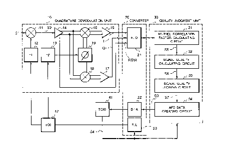
Fig. 1 is a block diagram showing the
5 constitution of an automatic frequency control circuit
according to the embodiment of the-invention.
As shown in Fig. 1, the automatic frequency
control circuit of the embodiment comprises an quadrature
demodulation unit 10 for receiving a GMSK (Gaussian
Minimum Shiftkeying) signal "S1" to quadrature-demodulate
the same, a quality judgment unit 30 for judging the
quality of the GMSK signal "S1", a converter 20 for
carrying out digital to analog or analog to digital
conversion of a signal between the quadrature
demodulation unit 10 and the quality judgment unit 30, a
temperature compensated crystal oscillation circuit
(TCXO) 41 for compensating the frequency of the GMSK
signal "S1" on the basis of a result of judgment by the
quality judgment unit 30, and a voltage controlled
oscillation circuit (VCO) 42. It is noted here that Fig.
1 shows only characteristic parts of the constitution in
the embodiment, while the description of the other
constitution is omitted.
The quadrature demodulation unit 10 includes
a mixer 11 for receiving the GMSK signal "Sl" converted
to a first intermediate frequency signal and converting
it to a second intermediate frequency signal, a frequency
2 1 73785
-- 10 --
demultiplier 12, a frequency demultiplier 13 for
quadrature-modulating the second intermediate frequency
signal so as to create an in-phase signal "I" and an
antiphase signal "Q", amplifiers 14, 15 and 17, mixers 16
and 18, and a phase shifter 19.
The GMSK signal ~S1" received and converted
to the first intermediate frequency signal by a mobile
communication receiver is supplied to the mixer 11. The
mixer 11 mixes a frequency divided signal by the
frequency demultiplier 12 with the GMSK signal "Sl" so as
to create the second intermediate frequency signal "S2".
A signal is supplied from the voltage
controlled oscillation circuit 42 to the frequency
demultiplier 12. The frequency demultiplier divides the
frequency of the signal by nl. The obtained
frequency-divided signal is transferred to the mixer 11.
It is noted here that nl is an arbitrary whole number.
Further, a signal is supplied from the
voltage controlled oscillation circuit 42 to the
frequency demultiplier 13. The frequency demultiplier 13
divides the frequency of the signal by n2. The obtained
frequency-divided signal is transferred to the phase
shifter 19. It is noted here that n2 is an arbitrary
whole number different from nl.
Provided at subsequent stages of the mixer 11
are the mixer 16 including the amplifier 14 at its input
side and the amplifier 15 at its output side, the mixer
21 73785
,
18 including the amplifier 14 at its input side and the
amplifier 17 at its output side, and the phase shifter 19
for converting the phase of the second intermediate
frequency signal "S2" supplied to the mixers 16 and 18.
The second intermediate frequency signal "S2"
is supplied from the mixer 11 to the mixer 16 via the
amplifier 14. The mixer 16 creates the in-phase signal
"I" having the same phase as the second intermediate
frequency signal "S2", and transmits it via the amplifier
15.
Also, the second intermediate frequency
signal "S2" is supplied from the mixer 11 to the mixer 18
via the amplifier 14. The mixer 18 creates the antiphase
signal "Q" of which phase is shifted at an angle of 90
with respect to the in-phase signal ~ supplied from the
mixer 16. The mixer 18 supplies the antiphase signal ~Q~
via the amplifier 17.
The phase shifter 19 shifts the phase of the
. second intermediate frequency signal "S2" supplied to the
mixer 18 at an angle of 90 with respect to the phase of
the second intermediate frequency signal "S2~ supplied to
the mixer 16, thereby creating the in-phase signal "I~
and the antiphase signal "Q".
The quadrature demodulation unit 10 transmits
to the converter 20 the in-phase signal ~I" and the
antiphase signal "Q" thus created, as well as an electric
field strength signal "RSSI" supplied from the amplifier
2~ 73785
- 12 -
14.
The converter 20 includes an A/D conversion
circuit 21, a D/A conversion circuit 22, and a PLL (Phase
Lock Loop) circuit 23.
The A/D conversion circuit 21 converts the
in-phase signal "I", the antiphase signal "Q" and the
electric field strength signal "RSSI" transmitted from
the quadrature demodulation unit 10 into digital signals
so as to send them to the quality judgment unit 30.
The D/A conversion circuit 22 converts into an analog
signal an automatic frequency-controlling data (referred
to as AFC data hereinafter) signal ~S3~ transmitted from
the quality judgment unit 30, which data will be
described below. The D/A conversion circuit 22 sends the
AFC data signal to the temperature compensated crystal
oscillation circuit 41.
The PLL circuit 23 controls the voltage
controlled oscillation circuit 42 on the basis of a
compensation signal "S4~ from the temperature compensated
crystal oscillation circuit 41.
The quality judgment unit 30 includes a
mutual-correlation factor calculating circuit 31 for
calculating the mutual-correlation of the input signals,
a signal quality calculating circu~t 32 and a signal
quality judging circuit 33 for judging the quality of the
input signal on the basis of the calculated
mutual-correlation of the input signal, and an AFC data
21 73785
- 13 -
creating circuit 34 for creating an AFC data in
accordance with the quality of the input signal.
The in-phase signal "I" and the antiphase
signal "Q" converted to the digital signals are supplied
to the mutual-correlation factor calculating circuit 31.
The circuits 31 calculates the mutual-correlation factor
of the input signal to compute an amount of interference
between codes. Concretely, the codes interference amount
is computed in the following manner. At first, in the
GSM(Global System for Mobile communication), central
continuous 16 bits among 26 bits of training sequence
codes in one burst of the in-phase signal ~ are shifted
across, thereby to obtain eleven mutual-correlation
factors. Arbitrary five mutual-correlation factors are
selected from the obtained eleven mutual-correlation
factors and the absolute values thereof are totalized.
Except for the five mutual-correlation factors having the
absolute values of which total is maximum, a total of the
absolute values of the other six mutual-correlation
factors is subtracted from a total of the absolute values
of all the eleven mutual-correlation factors. The
obtained value is supplied to the signal quality
calculating circuit 32 as the codes interference amount
signal "S5".
Essentially, the 16 bits corresponding to the
six mutual-correlation factors having the absolute values
whose total is m~x;mum, are positioned at the center of
2 1 73785
- 14 -
the 26 bits of the training sequence codes unless the
quality of the input slgnal is deteriorated. When the
input signal is degraded in quality, the above 16 bits
are shifted. Therefore, it can be detected by the above
operation whether the quality of the input signal is
deteriorated or not.
The signal quality calculating circuit 32
determines the quality of the input signal on the basis
of the amount of interference between the codes exhibited
by the codes interference amount signal "S5" supplied
from the mutual-correlation factor calculating circuit 31
as well as the electric field strength signal ~RSSI~. To
be concrete, the quality of the input signal is
determined as follows. That is to say, the signal
quality calculating circuit 32 has a table which relates
a combination of the codes interference amount and the
electric field strength signal ~RSSI~' to a numerical
value predetermined to represent the quality of the input
signal, with the codes interference amount and the
electric field strength signal ~RSSI~ as parameter. The
amount of interference between the codes of the input
signal exhibited by the codes interference amount signal
"S5" calculated by the mutual-correlation factor
calculating circuit 31 and the electric field strength
signal ~RSSI~ of the input signal supplied from the A/D
conversion circuit 21 of the converter 20 are combined
and checked with the table, and the corresponding
2 1 73785
- 15 -
numerical value is supplied to the signal quality judging
circuit 33 as a quality signal "S6" representing the
quality of the input signal.
The signal quality judging circuit 33
evaluates the quality of the input signal on the basis of
the quality signal "S6" from the signal quality
calculating circuit 32, and controls the AFC data
creating circuit 34. More specifically, there are
provided several ranks for evaluating the quality of the
input signal, and it is judged which rank the quality
signal "S6" of the input signal is in. A control signal
"S7~ for controlling the AFC data creating circuit 34 is
supplied in order to perform a predetermined compensation
to the AFC data in accordance with the quality rank of
the quality signal "S6".
The AFC data creating circuit 34 compensates
the AFC data on the basis of the control signal "S7" from
the signal quality judging circuit 33, so as to create
and supply the AFC data signal "S3". The output AFC data
signal "S3" is not only utilized by the mobile
communication system body, but also transferred to the
D/A conversion circuit 22 of the converter 20. The AFC
data is compensated by multiplying the AFC data by a
compensation factor previously set in correspondence with
every rank of the quality of the input signal.
A more detailed description will be made
about the judgment of the quality of the input signal by
21 73785
- 16 -
the signal quality judging circuit 33 and the
compensation of the AFC data performed by the AFC data
creating circuit on the basis of that quality judgment.
More specifically, the signal quality judging
circuit 33 fixes on the quality of the input signal
either of eleven ranks between "10" exhibiting the
highest quality and "0" exhibiting the lowest quality.
The AFC data creating circuit 34 regards the ranks "3"
and below as inferior quality and compensates the input
signal in the same manner when any of the ranks "3" and
below is fixed on the quality of the input signal. In
this case, if the signal quality judging circuit 33
decides that the quality signal "S6" delivered from the
signal quality calculating circuit 32 corresponds to the
rank "10", the signal quality is kept by 100%. The AFC
data creating circuit 34 multiplies the AFC data by a
compensation factor predetermined in accordance with the
quality. Then, the AFC data creating circuit 34 supplies
the AFC data signal ~S3" thus obtained.
In the case where the signal quality judging
circuit 33 judges that the quality signal "S6"
transmitted from the signal quality calculating circuit
32 corresponds to a rank ~7~, the signal quality is kept
by 70%. The AFC data creating circuit 34 multiplies the
AFC data by a compensation factor predetermined in
accordance with the quality. Then, the AFC data creating
circuit 34 supplies the AFC data signal "S3" thus
2 1 73785
obtained.
Further, if the signal quality judging
circuit 33 judges that the quality signal "S6"
transmitted from the signal quality calculating circuit
32 corresponds to the:rank "3", the signal quality is
kept by 30%. Because the AFC data-creating circuit 34
treats the quality in the rank "3" and below as the same
inferior quality, the AFC data creating circuit 34
multiplies the AFC data by a.compensation factor
predetermined in accordance with the quality in the rank
"0". Then, the AFC data creating circuit 34 supplies the
AFC data signal "S3" thus obtained.
Incidentally, how many ranks there provided
for evaluating the quality of the input signal and how a
compensation factor corresponding to each quality rank is
predetermined, can be appropriately decided in accordance
with the constitution or purpose of use of the mobile
communication system, the frequency of an input signal to
be dealt with by the communication system, or the like.
The AFC data signal "S3" converted to the
analog signal by the D/A conversion circuit 22 of the
converter 20 is supplied to the temperature compensated
crystal oscillation circuit 41. The circuit 41 transmits
the compensation signal "S4" on the basis of the AFC data
signal "S3". The compensation signal "S3" is supplied to
the PLL circuit 23 of the converter 20 to control the
voltage controlled oscillation circuit 42. The signal
2 1 73785
- 18 -
"S3'~ is also supplied to the quality judgment unit 30 so
as to be used as an operation clock for the respective
circuits 31 to 34.
A control voltage of the voltage controlled
oscillation circuit 42 is controlled by the PLL circuit
23, thereby to vary the oscillation frequency. Then, as
described above, the output signal of the voltage
controlled oscillation circuit 42 is supplied to the
frequency demultipliers 12 and 13, so that information of
the AFC data is fed back to the GMSK signal "S1-".
Referring to a flow chart of Fig. 2, an
operation of the embodiment will be described below.
When the received GMSK signal "S1" is
supplied to the mixer 11 of the quadrature demodulation
unit 10 (Step 201), the frequency demultiplying signal
from the frequency demultiplier 12 is mixed with the GMSK
signal "S1" so that the second intermediate frequency
signal "S2" is created (Step 202). After being amplified
by the amplifier 14, the second intermediate frequency
signal "S2" is supplled to the mixers 16 and 18. After
the phase of the second intermediate frequency signal
"S2" is shifted by the phase shifter 19, it is amplified
by the amplifiers 15 and 17 so as to be supplied to the
converter 20 as the in-phase signal "I" and the
~'antiphase signal "Q" (Step 203). The second
intermediate frequency signal ~S2~ is divided by the
amplifier 14 and supplied to the converter 20 as the
2 1 73785
electric field strength signal "RSSI " .
The in-phase signal "I", the antiphase signal
-Q-- and the electric field strength signal "RSSI"
supplied to the converter 20 are converted to the digital
signals by the A/D conversion circuit 21, so as to be
supplied to the quality judgment unit 30 (Step 204).
When the in-phase signal "I" and the
antiphase signal "Q" are supplied to the
mutual-correlation factor calculating circuit 31 of the
quality judgment unit 30, the amount of interference
between the codes is calculated on the basis of the
in-phase signal "I" and the antiphase signal "Q". The
codes interference amount signal 'S5-' representing the
result of the calculation is supplied to the signal
quality calculating circuit 32 (Step 205). Subsequently,
in the signal quality calculating circuit 32, the quality
signal "S6" representing the quality of the input signal
by a numerical value is created on the basis of the
amount of interference between the codes exhibited by the
codes interference amount signal "S5l' and the electric
field strength signal "RSSI", the quality signal 'S6--
being supplied to the signal quality judging circuit 33
(Step 206). Thereafter, the quality of the input signal
is ranked on the basis of the quality signal "S6"
supplied to the signal quality judging circuit 33. In
this connection, the control signal "S7" is supplied so
that the AFC data creating circuit 34 performs the
2 1 73785
-
- 20 -
compensation predetermined in correspondence to the rank
of the signal (Step 207). When the control signal "S7~
is supplied to the AFC data creating circuit 34, the AFC
data is compensated in response to the control signal
5 "S7~, so as to supply the AFC data signal(Step 208).
The AFC data signal "S3" created by the AFC
data creating circuit 34 is utilized by the mobile
communication system body, and also supplied to the
temperature compensated crystal oscillation circuit 41
after it has been converted to the analog signal by the
D/A conversion circuit 22 (Step 209).
Consequently, the compensation signal "S4"
corresponding to the AFC data signal "S3" is created in
the temperature compensated crystal oscillation circuit
41 and supplied to the PLL circuit 23 (Step 210). The
voltage controlled oscillation circuit 42 is controlled
on the basis of the compensation signal "S4" by the PLL
circuit 23, thereby carrying out the automatic frequency
control (Step 211).
As described above, according to the
àutomatic frequency control circuit of the present
invention, since the frequency is automatically
controlled on the basis of the result of judgment of the
signal quality by the quality judgment unit 30, even when
Doppler shift or multipass fading occurs during the
movement of the mobile communication system, the
frequency of the input signal can be compensated in
2 1 73785
- 21 -
accordance with the degradation of the quality of the
signal. Thus, it is possible to prevent the malfunction
of the mobile communication system such as stoppage of
the operation of the system.
Although the invention has been illustrated
and described with respect to exemplary embodiment
thereof, it should be understood by those skilled in the
art that the foregoing and various other changes,
omissions and additions may be made therein and thereto,
without departing from the spirit and scope of the
present invention. Therefore, the present invention
should not be understood as limited to the specific
embodiment set out above but to include all possible
embodiments which can be embodies within a scope
encompassed and equivalents thereof with respect to the
feature set out in the appended claims.