Note: Descriptions are shown in the official language in which they were submitted.
WO 95IlU9UU PCTlSE94l00909
~1'~~9~:~
TzTLE Or THE INVENTION: A SIGNAL RECEIVING AND A SIGNAL
TRANSMITTING UNIT
TECHNICAL FIELD
The present invention relates to a signal receiving and a
signal transmitting unit adapted to receive and further
transmit an information-carrying signal with no change in the
inforr,.ation content of the signal.
l0
The invention particularly relates to converting an informa
tion-carrying signal received at a first transmission rate to
an information-carrying signal which is transmitted at a
second transmission rate caith the same information content~as
the received signal.
DESCRIPTION OF THE PRIOR ART
Several diff~rc~t ;_inds o' signal receiving 4nd signal
transmitting uni is of the aforesaid kind are known to the art.
Different principles of converting the transmission rates of
signals through switches and like devices are known and
applied in 'the telecommunications field.
w It is also knocan, and standard, to use different transmission
rates, such as ? ~S Mb/s and 622 3~ib/s and also other transmis-
sion rates, such as 2.5 Gb/s, for instance.
Also known to the art are multiplexing signal receiving and
signal transmitting units in which signals received on a
connection have a signal transmission rate or 155 t~Ib/s and are
converted to a connection transmitted signal having a trans-
mission rate of 622 Mb/s.
Similar units are also known in which this rate conversion can
be effected from 155 Mb/s to 2.5 Gb/s.
SUBSTITUTE SHEET
~ '~ ~r~
Also known to the art are demultiplexing units in which the
signal transmission rate is converted from 622 Mb/s to 155
Mb/s, and so on.
Units of this kind are also known for conversion of other
signal transmission rates.
Normally, such units are adapted for one single conversion
index and each desired rate conversion requires a unit which
corresponds to the chosen rate conversion.
Consequently, several such units are required for different
purposes within switching equipment and other types of
electronic equipment.
With regard to the present invention and to its particular
application, it can be mentioned that a signalling pattern is
known in which information-carrying data packets, such as ATM
(Asynchronous Transfer Mode) cells, are transmitted, either in
series or in parallel, on each of a number of available
. connections.
A signalling pattern is also known in which a number of
available lines are adapted to the number of bit positions in
a word within a data packet, such as an ATM cell, and the
signal on each of these lines is permitted to carry the
content of respective bit positions simultaneously, wherein
a number of instantaneous bit positions occurring on these
lines together represent the signal information of a data
word.
The present invention can be applied advantageously in a
system described in Ericsson Review No. 1, 1993, in the
articles "The ATM Switch Concept and The ATM Pipe Switch" by
Mikael Larsson, et al, and "The Telecom Evolution in the
Broadband Era" by Peter Staxen, et al.
~~~!
.. .. . _. _".",. PCT/SE94lUU9U9
p _.
DISCLOSURE OF THE INVENTION
TECHNICAL PROBLEMS
When considering the prior art as described above, it will be
seen that a technical problem resides in the ability to
provide a novel signal receiving and signal transmitting unit
which is not only able to convert one single received informa-
tion-carrying signal to one single other transmitted informa-
l0 tion-carrying signal with a single specific relationship
between the transmission rates, but which caill also afford the
possibility of choosing one of a number of incorporated
transmission rates for received information-carrying signals
and enable the conversion of one such received signal to a
transmitted signal which, in turn, can be selectively allocat-
ed another transmission rate from a plurality of available
transmission rates.
It ::'ill also be seen teat a technical aroblem is o:~e oT
realizing that the use of such a unit having a plurality of
available signal receiving inputs where each input is adapted
to receive i.~.formation-carrying signals , such as data packets ,
at a transmission rate which differs from the transmission
rates of other inputs within a telecommunications system which
has different reauirements on transmission rates requires each
input to be connectable to an output for transmitting informa
tion-carrying signals, such as data packets, chosen from
several available outlets, :where each outlet is adapted to a
transmission rate which differs from the transmission rates
of remaining outlets.
Another technical problem is one of realizing and implementing
in a simple manner the choice of one conversion method from
a number of available conversion methods for multiplexing or
der~ultiplexing purposes.
A further technical problem is one of realizing that the
SUBSTITUTE SHEET
r. v !Ji a Vyvv rl. 1 ~Jr.y-lWUyvy
21'~~~~9
choice of conversion node can be nade in accordance with the
control signals occurring on one or more control lines, where
a selected control line and/or the signal informa~ion of a
control signal will initiate and select a conversion node with
a chosen conversion index related to the transmission rates.
It will also be seen that a technical problem resides in-
realizing that a signal receiving and a signal transmitting
unit which has successfully solved one or more of the afore-
said technical problems finds particularly suitable applica-
tion when a received information-carrying signal and a
transmitted information-carrying signal are comprised of
packets of data cihere each packet includes at least an
addressable part and an information-carrying part and can
therefore be included advantageously in an ATM system.
It caill also be seen that a technical problem resides in
realizing the significance of and the consequences associated
caitra adapting avail able i nputs an d avail able outpiit.~ =Oi: a~
determined conversion relationship between selected transmis-
sion rates such that the conversion ratio is changed, in-
creased or decreased, by a factor of "four" and therewith
realize and utilize the advantages of being able to reduce or
to increase the number of lines by a factor of "four".
It caill also be seen that a technical problem resides in
realizing the significance of and the flexibility afforded by
constructing a unit in cahich available inputs and available
outputs are structured for three different transmission rates.
A technical advantage is also achieved when respective inputs
and outputs in a unit of this kind are adapted for signal
transmission, or traffic, in each of two directions.
Another technical problem is one of realizing the advantages
that are afforded with the use of a signal receiving and
signal transmitting unit of the aforesaid kind which forms a
SUBSTITUTE SHEET
WO 951l0900 PCT/SE94100909
21'~~~~~~
mul ~ipieving/demultipiexing bloc): adapted for digital signals
and which is constructed and coordinated to convert a data
packet received at a low transmi ssion rate to a trars:~i ssio:.
rats which is four times hiaher than the received transmission
.. rate, or vice versa.
In this regard, a technical proble:~ resides in realizing the
adva:~tages that are afforded cahen conversion of the signals
or t:~e data packets is e'fected in a first stage, in a series-
parallel conversion stage, and the signals or the data packets
are :.hereafter stored in a memory store whose content can be
delivered to a parallel-series converter caith cloc:: pulse
COI7Ve=sion, t:~rough the medium of one er rore buffer circuits.
1~ Another technical problem is one c= realizing the need for the
reauisite memory store and the used buffer circuits to be
util_zed commonly for each signal data racket transmission,
irrespective cF the transni_ssion cirec t.ioil ciZOSen , and u? so
i n real izi:.g the advanzanes Lha t ~:i a of forded hereby .
Another tec: :.ical problem is one o. reali zing the significance
when receiving data packets or data cells that occur simulta-
neouslv on a number of _r.ccning ~nes in accordance wi t: the
two =arlie= shown sianallinc eatzerns of convertinc zhe
infer::,ation content of the data cells or data packets to a
parallel for~~sat that can be used internally in the unit.
Another technical problem is one o= realizing the simpli~ica-
tions that can be expected when tn2 frequenc,,% and/or rate of
the cock pulse is chosen at a spec=fic value below the values
that e:tist when receiving and trans-~ittirg a data cell on the
inpu_~ aid c~~~u~s c. the uni~ res~ectivelv.
A f;:= ch2r technical problem is one cf realizing the advantages
3~ that are afforded by the cccurrence of signal information in
the =crm cf data packets in an internal parallel format, with
the ~=oresaid presumptions accciuing to which the same
SUBSTITUTE SHEET
WU 95/lU9UU PCTISE94I00909
21'i 394
_. 6
synchronizing logic, memory stores, buffer circuits, etc., can
be used to selectively connect an available input from a
plurality of available inputs to an available output from a
plurality of available outputs.
Another technical problem is one of providing a data-t~acket
signal receiving and a data-packet signal transmitting unit
having a number of inputs for receiving data packets that have
different transmission rates and a number of outputs for
transmitting data packets at different transmission rates,
wherein one input unit can be used as an output unit and an
output can be used as an input.
In regard of a uni t of t:~e kind defined i :~ the introduction
1~ it will also be seen that a technical pronlem resides in the
creation of conditions with the aid of simple means such as
to adapt the total signal bandwidth of transmitted signals to
the total signal bandwidth of recei~Ted =_iar.~1=.
SOLUTION
t~dith the intention of solving one or more of the aforesaid
technical problems, the present invention takes as its
starting point a data packet receiving and data packet trans-
2~ mitting unit which is adapted to convert an information-
carrying digital signal received at a first transmission rate
to an information-carryi ng digital signal which is transmitted
at a second transmission rate different to the first transmis-
sion rate, said information-carrying digital signal being
adapted particularly for Lse with an AThi system in which the
information in transmitted signals is advantageously in the
form of a number of data packets each of a standard format.
The present invention relates to a unit, an integrated
circuit, an ASIC circui t having a plurality of available
inputs for'receiving digital signals, wherein each input is
adapted to a transmission rate which is different from the
SUBSTITUTE SHEET
w v ym tuyuu PCT7SE9a/00909
__ 7
transmission rates of other inputs. Each input can be connect-
ed to a signal transmitting output chosen from one of several
available outputs adapted for digital signals, and wherein
each output is adapted to a transmission rate which differs
from the transmissien rates of other outputs. The choice of
input arid output is made in accordance with signals occurring
-an one er several control lines or conductors, wherein a
selected control line and/or selected signal information
chooses and initiates one of several available conversion
modes with a selected rate conversion index.
According to proposed embodiments of the invention, the
received information-carrying signals and transmitted informa-
tion-carrying signals have the form of data packets or data
Z5 cells, such as data packets or data cells wfiose signal content
is adapted to an ATM system, wherein each packet includes at
least an addressable part and an information-carrying part.
Accerdi rg to o:.e ambodi ment ( available inputs and available
outputs are adapted so as to clearly transfer::t the transmis-
sion rates therebetween, such as increasing or decreasing the
transmission rates by a factor of "four", caith the number of
lines en inputs and outputs therewith being decreased or
increased by a zactor of "four".
According to another embodiment, available inputs and avail-
able outDUts within the unit are "three" in number and are
structured for three different transmission rates.
According to the invention, respective input units and
respective output units are adapted for separated traffic in
both directions.
Particular reference is made to a number of multiplexing/de-
multiplexing blocks which.are intended to convert received
digital signals which have low transmission rates to a rate
which is four times greater than the 10t5 transmission rate,
SUBSTITUTE SHEET
.. v r~muyuu YCT/SE9.ilUU9lly
c
while retaining the signal bandwidth.
The relevant conversion cf the data signals will preferably
be effected in a first stage in a series-parallel conversion,
where~r. the signals are stored in a memory and can be deliv-
ered from the memory to a parallel-series converter having a
clcck pulse converter for transmission, through the medium of
an array of buffer circuits.
The requisite memory and buffer circuits can be used for
signal transmission in each of two directions.
According to another embodiment, data cells that are received
and that occur on a number of lines are converted to an
1~ internal parallel format adapted to the unit, which, in turn,
is selected commonly for a11 available inputs and all avail-
able outputs, ~,~therein in the case of requisite signal process-
ing through the internal parallel format, zhe interna.: clock
pulse ~-a to i s chosen at a ? ower ~Tal ue than the clock pulse
rate and transmission rate of signals occurring on the inputs
and/or the outputs.
One and the same synchronizing logic, such as memories, buffer
circuits, control logic, coil l preferably be used when connect-
ing one of several available inputs to one of several avail-
able outputs.
ADVANTAGES
Those advantages that are primarily afforded by a signal
receiving and signal transmitting unit according to the
present inventicn reside in the construction of a single unit,
an integrated circuit, an ASIC circuit, which presents a
plurality of available inputs for receiving digital signals,
3~ wherein each input is adapted to a transmission rate which
differs from the transmission rates of remaining inputs, and
a plurality of available outputs for transmitting digital
SUBSTITUTE SHEET
signals, wherein each output is adapted to a transmission
rate which differs from the transmission rate of remaining
outputs.
Each of these inputs can be connected to one of the
digital-signal transmitting outputs. This enables one and
the same unit, an integrated circuit, and particularly an
ASIC circuit, to be used in different telecommunications
equipment. A conversion mode desired for a particular
1o application and having a selected conversion index can be
chosen by activating one or more control conductors. A
selected control conductor and/or selected signal
information initiates selection of the conversion mode.
Therefore, broadly stated, the invention provides a signal
receiving and signal transmitting unit for converting a
first transmission rate of a received information-carrying
signal to a second transmission rate of a transmitted
information-carrying signal that is different from the
2o first transmission rate. The unit comprises a plurality of
signal receiving inputs for receiving information-carrying
signals, wherein each input is structured to receive
information-carrying signals at a different rate, and a
plurality of signal transmitting outputs for transmitting
information-carrying signals, wherein each output is
structured to transmit information-carrying signals at a
different rate. At least one control conductor is provided
_ g _
for supplying control information indicative of a
conversion mode to be applied to the received information-
carrying signals. Control logic receives the control
information and selects a corresponding conversion mode, a
memory receives information-carrying signals from the
inputs, and a buffer circuit receives the information-
carrying signals from the memory and outputs the
information-carrying signals to the signal transmitting
outputs under control of the control logic. The control
logic connects one signal receiving input to one signal
transmitting output based on the control information, and
the unit performs rate conversion, using the control logic,
the memory and the buffer circuit, in the selected
conversion mode.
Alternatively summarized, the invention provides a signal
receiving and signal transmitting unit for converting a
first transmission rate of a received information-carrying
signal to a second transmission rate of a transmitted
2o information-carrying signal that is different from the
first transmission rate. The unit comprises a plurality of
signal receiving inputs for receiving information-carrying
signals, wherein each input is structured for a different
transmission rate, and a plurality of signal transmitting
outputs for transmitting information-carrying signals,
wherein each output is structured for a different
transmission rate. At least one control conductor is
- 9a -
_.
provided for supplying control information indicative of a
conversion mode to be applied to the received information-
carrying signals. A number of multiplexing/demultiplexing
blocks convert the first transmission rate of the received
information-carrying signal to the second transmission rate
of the transmitted information-carrying signal. The unit
connects one signal receiving input to one signal
transmitting output depending on the control information,
and the unit performs conversion, using the multiplexing/
to demultiplexing blocks, in a conversion mode having a
conversion index that is selected and initiated by the
control information.
BRIEF DESCRIPTION OF THE DRAWINGS
An exemplifying embodiment of a unit having features char-
acteristic of the present invention and at present prefer-
red and which is adapted for use in a telecommunications
system, particularly in an ATM system, will now be
2o described in more detail with reference to the accompanying
drawings, in which:
Figure 1 illustrates the principle construction of a
telecommunications system which utilizes ATM
technology;
Figure 2 illustrates schematically serially occurring data
packets or data cells used in the ATM system
according to Figure 1;
- 9b -
y~P
4'''~~~1
WU y~llUyUU PCT/SE94/UU9lly
to ~1'~~~~~
Figure 3 illustrates schematically the physical orientation
of circuit boards for the two coupling planes of
the coupling core, and circuit boards for the
connecting devices disposed in a magazine;
Figure 4 illustrates schematically the orientation of cor-
responding circuit boards in an extended telecom-
munications system according to Figure 1, wherein
redundant boards for the coupling core are coordi-
hated in two magazines, whereas the circuit boards
for the connecting devices are coordinated in four
magazines;
Figure 5 illustrates the principle coupling required betcaeen
two redundant coupling or conri~ction planes each
allocated a respective magazine, and four magazines
for circuit boards applicable to the connecting
de Jices ;
Figure 6 is intended to illustrate an optical connection,
available from a plurality of optical connections,
between a switch coupling plane and a magazine
intended for circuit boards ret~resentative of
connecting devices;
Figure 7 illustrates the principle construction of a signal
receiving and signal transmitting unit in accor-
dance with the present invention;
Figure o is a block sche:~atic illustrating a Bi-Ci~iOS inte-
grated circuit for certain parts of the unit,
including rive nultipiexing/demultiplexing blocks
among other things; and
Figure 9 is a block schematic illustrating such a block,
cahich includes CldOS transistors .
SUBSTITUTE SHEET
wu y5iluyuu PCT/SE9410U909
11 ~1'~3~~9
DESCRIPTION OF EXEMPLIFYING EMBODIMENTS AT PRESENT PREFERRED
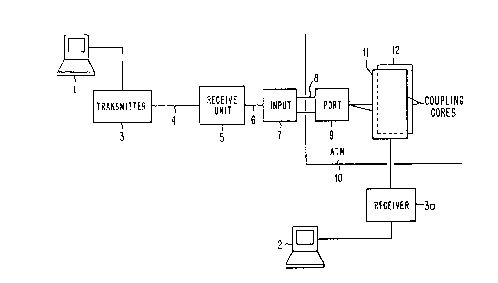
Figure 1 is a greatly simplified illustration of a telecommu-
nications system designated an ATI~i system, which utilizes data
coordinated in data packets or data cells for its function and
its signal exchange.
It will be obvious to the person skilled in this art that the
signal exchange is normally two-directional, although for the
sake of simplicity the following description will illustrate
solely the connection and signal-exchange between a transmit-
ter 3 of a transmitting terminal apparatus 1 and a receiver
3a of a receiving terminal apparatus 2.
1~ The exchange of information between the apparatus 1 and 2 is
achieved with the aid of data packets or data cells (20) with
data words structured in accordance with an ATri system.
The transmitter 3 coacts over a line or connection 4 with a
line-related receiving unit ~ which is connected via a line
or connection 6 to an input circuit 7 and which coacts,
through a line or connection 8, with a number of coupling
ports 9 belonging to an ATI~i switch 10 provided with two
redundant coupling planes or coupling cores 11, 12, and which
coacts with the signal receiving unit 3a through the medium
of circuits ( not shown ) corresponding to the circuits 9 , 7 and
5.
Each of the lines 4, G, 3 may consist of one or a nunber of
physical conductors.
The function of the AThi switch requires signal transinission
to be effected in packets or cells of data, and Figure 2
illustrates one such packet 20 which may have a five-byte (8-
bit words)~.address information section 21 (Header) and a
forty-eight'-byte (8-bit words) information-carrying section
22 ( Payload) . The data cell 20 may also include other informa-
SUBSTITUTE SHEET
.. v y~muyuu PCT/SE94/00909
12 ~~~3~~~
tion.
It should be noted that when transmitting signals on one
singl a physical conductor, one data cell, 20, will be preceded
by a data cell 20' and followed by a data cell 20", caherewith
a serial strean of data packets or data cells will pass along
the conductor 4.
It .s also assumed that the line ~, together with its conduc
toys, is dimensioned and adapted to a serial bit-rate of 155
t~ib/s ec .
Such serial signal transmission oz data cells is referred to
as "series transmission" in the following description.
cahen a similar "series transmission" takes place simultaneous-
ly on a plurality of conductors forming a line, this transmis-
sion is referred to as a "series transmi:;si.nn through oro!iped
links".
However, each word in a data cell can be transmitted simulta-
neously over a number of conductors, with the number of
conductors corresponding to the number of bit positions in
each word used, so that the bit information for a complete
word is received simultaneously by a nunber of receivers.
,:a;:
,.,~,
Such parallel transmission of data cells is referred to in the
following as "parallel transmission".
Figure 3 illustrates the principle, physical construction of
circuit boards placed in a magazine 30 which serves a switch
unit l0 or ATt~i s:~itch of relatively low capacity.
Located at the sides or extremities of the magazine is a
respective board 31 and 32, both of which are identical to one
another and' are provided with conductors and components corre-
sponding to the switch planes or selector planes 11 and 12.
SUBSTITUTE SHEET
w v ym iuyuu PCT/SE94/UU9tly
21'~33~~
.13
Located between these end boards 31 and 32 are a number of
boards which are adapted to form connecting devices, of which
six such boards are shown and of which two have been refer-
enced 33 and 34 in Figure 3.
The device boards 33, 34 are constructed to include circuit
structures pertinent to the input circuit 7 and the coupling
port 9. Conductors and buses are connected to respective
boards 33, 34 and 31, 32 by means of pin connectors. The pin
connectors of respective boards coact with circuitry (not
shown) mounted in a frame 35 or a backplane.
As will be understood, if it is desired to greatly increase
the capacity of a switch 10 with regard to the number of
simultaneous telecommunication connections, it is also
necessary to increase the rate at which signal transmission
is effected within the switch.
A contemplated increase in the capacity of the switch is
illustrated by choosing two magazines 40, 40a where al l boards
disposed in the magazine 40 can be considered to represent the
switch plane 11, while a11 boards disposed in the magazine 40a
can be considered to represent the switch plane 12.
Also included are four other magazines 41, 42, 43, 44, which
coact with the magazines 40, 40a in the manner illustrated in
Figure 5, in other words, each magazine 41) 42, 43, 44 coacts
with the two switch planes 40, 40a through a connection. It
will be evident that such a construction will require compre-
hensive signal transmission at a high transmission rate.
Signal transmission on each line and on each conductor takes
place at a high data-pulse rate, wherein typical pulse
frequencies are the standardized transmission rates of 155
Mb/s and 622 ?~ib/s . .
As the signal transmission can, in principle, be considered
SUBSTITUTE SNEET
YI.I~JGy-mvwm
wV y~llU'JUU
~~1~~~~
'14
the same for a11 of the connections shown in Figure 5, the
following description will be restricted solely to include
signal transmitting and signal receiving circuits for digital
pulses on one line or one connection 50 comprised of a fibre
optic and functioning to effect signal transmission between
the magazine 41 and the magazine 40 of the Figure 6 illustra-
tion.
The magazine 41 includes a number of integrated circuits on
i0 which there is mounted a number of signal muitiplexing/demul-
tiplexing blocks, of which one is referenced 61 and which are
connected to a transmitter 62 which is adapted to transmit
light pulses on the optical link or conductor 50 in response
to output signals from the block or the device 61.
-r
The light pulses on the line or conductor 50 are received by
a receiver 63 which is adapted to receive the light pulses and
to convert said light pulses to electric signals or electric
pulses.
These electric pulses are delivered to one of several avail-
able multiplexing/demultiplexing blocks 64.
The present invention also includes a particular design of one
such block 61 or 64.
The block 61 and the block 64 are mutually identical and
consequently the following description will be limited to
solely the block 61, with transmission of the data signal at
a higher transmission rate than the rate of the received data
signals.
The principle construction, as an integrated circuit, of one
such multiplexing/demultiplexing block 61 will now be de-
scribed in'more detail with reference to Figures 7, 8 and 9,
whereafterl the use of the block in the circuit shown in Figure
6 will be described more thoroughly.
SUBSTITUTE SHEET
. .. .." .". "" YC:'1~/SF;'l4/UUyUy
21'~3~~~9
Figure 7 illustrates the principle construction of a multi-
plexing/demultiplexing block 61 or unit according to the
present invention.
5 As shown in Figure 7, synchronizing signals are delivered to
the block 61 on a conductor 70a, while clock pulses arrive on
a conductor 70b, the effect of these clock pulses being well
known to the person skilled in this art and will not therefore
be described here.
It can be mentioned in this regard that the block 61 may well
be provided with means for generating internal synchronizing
signals.
The block 61 is constructed to include three different inputs,
referenced 70c, 70d and 70e, and three different outputs,
referenced 70c', 70d' and 70e'.
Each of the inputs is adapted for receiving information-
carrying digital signals in data cells having mutually
different transmission rates.
Each of the outputs is adapted for transmitting information
carrying digital signals in data cells at different transmis
sion rates.
More particularly, the input 70c and the output 70c' are both
adapted for a transmission rate of 155 Mb/s.
The input 70c and the output 70c' are both comprised of
sixteen conductors, wherein the data packets are transmitted
on each of these conductors serially and together form a
series transmission through grouped links.
The input 70d and the output 70d' are both adapted for a
transmission rate of 622 2~ib/s, wherein they are each comprised
of four conductors and the data packets occur on each of said
SUBSTITUTE SHEET
wV yJ/lUyUU PCT/SE94/00909
21'~3g~9
16
conductors serially and together form a series transmission
through grouped links.
The input 70e and the output 70e' are both adapted for a
trans::~ission rate of 2.5 Gb/s and are comprised of or.e single
conductor adapted for transmitting data packets or data cells
serially in sequence.
According to the invention, such a unit is able to freely
select a conversion mode through the medium of a control
signal, such that each of the three available inputs 70c, 70d
and 70e can be connected to an output selected from the three
available outputs 70c', 70d' or 70e'.
The choice of a specific input and a specific output, the so-
called conversion mode, is effected in accordance with signals
that occur on one or more control conductors 71, =.aherein a
selected control conductor and/or signal-carri~3 i~~=creation
initiates a circuit 72 ~~~hich selects the relevant conversion
mode through the medium of a control block 93 with a selected
conversion index adapted for a specific application.
The placement of such a unit or block 61 in switch equipment,
or elsewhere, thus becomes more or less determinative of which
;..,:
<<;;;~>' 2~ conversion mode shall be selected and be applicable to the
selected application.
Figure 8 is a block schemati c which illustrates the nultiplex-
ing/demultiplexing block 61 of Figure 7 in more detail.
The block G1 is constructed on a digital Bi-CtlOS circuit and
utilizes a Ci~iOS section 80 ~Nhich is laid on said circuit and
has four mutually identical sub-blocks 81, 81a, 81b and 81c.
The input 7pc includes four input conductors for the sub-block
81, four input conductors for the sub-block 81a, and so on,
making a total of sixteen conductors.
SUBSTITUTE SHEET
w v ramvrvv YI.I~JGJ'r~uV7Vl
~7 ~1'~3~4~
The sub-blocks 31, 81a , 81b and 81c are also provided with
four times four output conductors 70c'.
Each of the sub-blocks 81, 81a, 81b and 81c has a respective
output conductor, such as the conductor 83 for the sub-block
81.
A11 four output conductors 33, 83a, 83b and ~3c forn input
conductors to a fifth sub-block 84 which, in principle, is of
the same construction as the sub-block 81.
The sub-block 84 includes four input conductors 70d, four
output conductors 70d' and an output conductor 70e'.
In the case of the Figure 8 illustratiol~f, the block 61 is
adapted for a multiplexing and a demultiplexing function,
caherein in the case of the multiplexing function data signals
occurrinct on the input 70c have a rate of 1S5 :~ib/s, whils data
signals occ~,~rring on the outputs 83, 83a, 83b and 83c have~a
rate of 622 ldb/s .
Signals occurring on the output 70e' of the sub-block 84 have
a rate of 2.5 Gb/s.
The signal =low travels in the opposite direction in the case
w of a demultiplexing function.
Figure 9 is a block schematic which i .ustrates the sub-block
81 in more detail.
The input conductors 70c are repr-~ented in the Figure 9
illustration by the four incoming conductors 82a ... 82d.
Each of the conductors 82a ... 82:is adapted for a maximum
transmission rate of 155 M,b/s for data packets in the form of
ATM cells used in this case.
SUBSTITUTE SHEET
vv V YJ/ IUyUU P~ ris~yamoyuy
1.8 2~ r 3~~~
The circuit 95 is able to transmit data-containing output
signals at a frequency of 622 Mhz on the conductor 83, with
the aid of a series-parallel converter 91 and a memory 94
among other things.
It has previously been mentioned in the description that each
of the inputs 70c, 70d and 70e and each of the outputs 70c',
70d' and 70e' can be coupled selective? y so as to obtain a
desired rate conversion, and that a relevant conversion mode
is activated by an activating signal arriving on one or more
of the conductors 71 (Figure 8).
System-related clock pulses occur on the conductor or line 87.
Referring back to Figure 9, it will be seen that each of the
input conductors 82a ... 82d of the sub-block 81 is connected
to a series-parallel converter 91. The digital signals
arri~ing or. tze conductors 82a ... 82d thus converted by a
four-channel series-parallel converter to 20-bit parallel
transmission, t.~herein the signals are delivered on a conductor
or line 99 to a control logic 93 where they are processed at
an internal rate.
Requisite synchronization is effected through a synchronizing
unit 98.
Data signals converted to a parallel format are delivered to
a control block or control logic 93 and from there to a memory
94, a RAM memory. Information stored in the RAM memory, is
delivered therefrom, or from a ROM memory, through control
logic 93 to a buffer circuit 95, which in turn delivers the
information to a single-channel parallel-series converter and
clock pulse converter 96.
When converting in the reversed sense, signals arrive on the
conductor 83' to a single-channel series-parallel converter
and clock pulse converter 97, whereai'ter data signals in
SUBSTITUTE SHEET
wv yaituyuu PCT/SE94/00909
.~ 19 21'~3~~~~
parallel format are delivered to the control block 93, stored
in the memory 94 and then delivered in parallel format to the
buffer circuit 95, whereafter they are transmitted to a
parallel-series converter 92 and fed out on the conductors
a2~.
The exemplifying embodiment illustrates the invention in the
form of a functional block, and since such blocks are previ-
ously known or can be constructed readily by the skilled
person in this field without reauiring work of an inventive
nature, and with the guidance of general technology in the
field and with the aid of obvious expedients, certain parts
have not been described in detail.
With regard to the signals on the conductor 71, it is assumed
that parallel-transmitted bit positions on the three conduc-
tors of relevant bit configuration point to the relevant
conversic~ mode.
This bit configuration is transmitted to each of the control
logic circuits, for instance circuit 93, which therewith
calculates and selects the necessary signal flow and conver-
sion node.
It will also be noted that the clock pulse rate for the
internal signal processing is about 30 Mhz.
A signal receiving and signal transmitting unit of the
aforedescribed kind can be used advantageously with a circuit
arrangement described and illustrated ?n a Patent Application
filed on the same date as the present Application and entitled
"A Signal Processing Unit", or a unit described and illustrat-
ed in a Patent Application filed on the same day as the pre-
sent Application and entitled "A Multiplexing/Demultiplexing
Unit", or in an arrangement described and illustrated in a
Patent Application filed on the same day as the present Appli-
cation and entitled "A Synchronizing Circuit Arrangement".
SUBSTITUTE SHEET
TYV 7JILV7uu
rL 1 i~t,y~/uuyuy
~_ 2 0
Reference is made to these coterminous Patent Applications for
a deeper understanding of the application of the invention,
and the contents of these ADblications shall be taken to form
part of the present Application.
It caill be understood that the invention is not restricted to
the aforedescribed and illustrated exemplifying embodiment
thereof and that modifications can be made within the scone
of the inventive concept as illustrated in the following
Claims.
SUBSTITUTE SHEET