Note: Descriptions are shown in the official language in which they were submitted.
IMAGE DISPLAY APPARATUS WITH FLAT SCREEN
FIELD OF THE INVENTION
This invention relates to an image display apparatus having
multilayer structure comprising a flat panel, an adhesive resin layer
and a front panel, and a method of manufacturing the same.
BACKGROUND OF THE INVENTION
Examples of conventional image display apparatus include cathode
ray tubes, liquid crystal panels and a plasma displays. In general,
a cathode ray tube has a curved-shaped image display screen.
However, a cathode ray tube having a flat image display screen which
provides an image display with high resolution and less distortion
over the whole screen are used as computer displays and the like.
Many of the front panels which are layered on the flat panel through
an adhesive resin layer serve not only a reinforcement function for
the image display screen but also an anti-reflection function against
outside light and an anti-static function. In general, an image
display apparatus having multilayer structure comprising a flat
panel, an adhesive resin layer and a front panel is manufactured as
follows. First, spacers are placed at a flat panel portion, a front
panel is placed on the flat panel, and the gap at the periphery
between the flat panel and the front panel is sealed by using resin
tape or resin for sealing having a high viscosity. The gap at the
periphery between the image display screen and the front panel is
filled by injecting adhesive resin having a low viscosity from an
opening that is formed in the periphery of the flat panel and the
- 1 -
front panel. Then, the adhesive resin is hardened, and as a result,
an image display apparatus having multilayer sturcture comprising a
flat panel, an adhesive resin layer and a front panel is
manufactured. (For example, refer to Japanese Un-examined Patent
Publication N0. Hei 6-20598.)
However, the above-mentioned manufacturing method has following
problems and is required to be improved.
First, in a method for sealing a gap between the flat panel and
the front panel by using a resin for sealing having a high viscosity,
a step of hardening resin by irradiating ultraviolet rays or heating
that usually needs 30 to 90 minutes is required twice for the sealing-
resin and the adhesive resin.
Second, in sealing, the image display screen has to be
maintained horizontally. However, in injecting adhesive resin in a
gap at the periphery between the flat panel and the front panel, the
image display screen has to be tilted. Therefore, in attaching the
front panel to the flat panel of the image display apparatus, two
kinds of structures, maintaining the image display apparatus
horizontallly and maintaining the image display apparatus in a
position tilted at a certain angle are required.
On the other hand, in a method for sealing a gap at the
periphery between the flat panel and the front panel by using resin
tape, sealing is not completed sufficiently, and the adhesive resin
might leak out before hardened.
In addition to that, there are the following problems concerning
production efficiency that apply to both of the above-mentioned
methods. First, it takes a long time to inject adhesive resin in a
- 2 -
217~~22
narrow gap that is formed between the flat panel and the front panel.
Second, bubbles are easily formed in the adhesive resin layer.
Third, control of the viscosity of the resin is required strictly for
the resin to be filled completely in the whole area.
SUMMARY OF THE INVENTION
In order to solve the above-mentioned problems, this invention
aims to provide an image display apparatus having multilayer
structure comprising a flat panel, an adhesive resin layer and a
front panel and a method of manufacturing the same efficiently.
According to the image display apparatus of the invention,
contamination caused by the adhesive resin, and defective qualities
such as deterioration, discoloration, and peeling of the adhesive
resin do not tend to occur.
According to the invention, an image display apparatus having
multilayer structure comprising a flat panel, an adhesive resin layer
and a front panel is provided. The above-mentioned multilayer
structure is formed by forming the adhesive resin layer on the
surface of the flat panel and then gluing the front panel thereto.
In addition to that, the invention provides a method for
manufacturing an image display apparatus having multilayer structure
comprising a flat panel, an adhesive resin layer and a front panel,
the method comprising a step of applying adhesive resin to the
surface of the flat panel, a step of gluing the front panel to the
adhesive resin layer and a step of hardening the adhesive resin.
According to the present image display apparatus and the method
of the manufacturing the same, the above-mentioned problem, which is
- 3 -
2~~~~zz
caused by injecting adhesive resin in a narrow gap between the flat
panel and the front panel are facing each other through the spacer
does not occur.
It is preferable that in gluing the front panel to the adhesive
resin layer, one side of the front panel which is tilted toward the
flat panel and is contacted to the adhesive resin layer. Then the
front panel is tilted gradually to become parallel to the flat panel
and then the front panel is pushed toward the flat panel. According
to the above-mentioned method, bubbles are not easily formed in
adhesive resin layer between panels and the formed bubbles are
escaped from the gap of the panels easily with excess adhesive resin.
It is also preferable that, in applying the adhesive resin, the
thickness of the adhesive resin layer decreases from the one side to
which the side of the front panel is first contacted to the opposite
side, so that the formed bubbles do not remaine between panels.
It is also preferable that the step of applying adhesive resin
is performed at a temperature that is higher than room temperature so
as not to cause peeling of adhesive resin after hardening, or under a
condition in which the temperature of the surface of the flat panel
is maintained between 30 to 50 °C . Further, an ultraviolet ray
hardening resin or heat hardening resin may be used as the adhesive
resin.
It is also preferable that a pressing plate having a circular or
an oval shape is used to press the flat panel to the front panel.
The pressing of the front panel is intended to remove formed bubbles
from the gap between the panels and obtain the predetermined
thickness for the adhesive resin layer. Further, in pressing the
- 4 -
~~7~s2z
front panel to the flat panel, the pressing plate having a
rectangular shape which is same as that of flat panel or front panel
may be used, however, a more uniform thickness of the adhesive resin
layer can be obtained by using a pressing plate having a circular or
an oval shape.
In particular, it is preferable that an image display apparatus
comprising a cathode ray tube has a construction as follows.
The image display comprises a cathode ray tube comprising a bulb
having a flat glass panel portion, a flat shadow mask which is formed
facing the inner side of the flat glass panel portion and a
reinforcement band that is fixed at the periphery of the flat glass
panel portion.
The flat glass panel portion is formed integrally with a flat
panel for displaying an image and a glass wall portion that is
formed perpendicularly from the edge of the flat panel to connect
with the funnel portion.
The above-mentioned flat shadow mask is supported with tension
by a frame which is attached removably to an inner side of the glass
wall portion.
The above-mentioned structure of the cathode ray tube is
preferable not only for the manufacturing method in which a front
panel is attached to after the adhesive resin layer is formed on the
surface of the flat panel, but also for the strength of the image
display screen having a flat surface. That is, the flat panel and
glass wall portion are formed integrally and the glass wall portion
is connected to the funnel portion. As a result, the breaking
strength of the connected portion is much stronger with respect to
- 5 -
21'~~822
the pressure that is applied to the image display screen from outside
than in the case which the periphery of the flat panel is connected
with the funnel portion directly. In addition, the mechanical
strength with respect to the pressure from outside is improved by a
reinforcement band which is fixed at the periphery of the glass panel
portion (glass wall portion).
It is also preferable that the above-mentioned reinforcement
band is extended from the surface of the flat panel. By use of the
above-mentioned extruded reinforcement band, in applying adhesive
resin to the surface of the flat panel, leak of the adhesive resin of
the glass wall portion is prevented.
It is also preferable that a reservoir is formed for the
adhesive resin which is leaked from the periphery of the front panel
is formed in the periphery of flat panel along with protection means
covering the exposed portion of the reservoir for the adhesive resin.
It is preferable that the above-mentioned front panel (or
adhesive resin layer) has enough conductivity for preventing the flat
panel from being charged and also has a function is preventing
reflection of outside light (including a function to diffuse
reflection).
In a method of gluing the front panel to the adhesive resin
layer, it is preferable that, before a step of applying adhesive
resin to the surface of the flat panel, a reinforcement band is fixed
at the periphery of the flat panel and extended from the surface of
the flat panel. The surface of the flat panel is polished, the
surface to which the front panel is attached is finished, and a wall
for prevention of leak of adhesive resin is formed around the
- 6 -
~17~:~2~
reinforcement band extended from the front edge of the reinforcement
band.
In addition to that, after the step of hardening the adhesive
resin, it is preferable that the surface protective sheet of the
front panel is removed and a protective treatment to cover the
surface of adhesive resin that is leaked from the front panel portion
with resin tape is performed. By performing the above-mentioned
treatment, an appearance is improved, and derioration and
discoloration of adhesive resin caused by the elapse of time can be
prevented.
BRIEF DESCRIPTION OF DRAWINGS
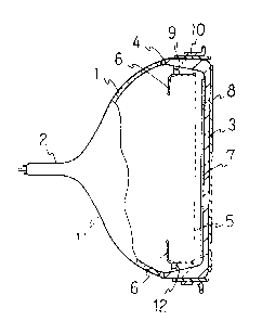
FIG.1 is a sectional view showing an image display apparatus of
the invention seen from the side of the cathode ray tube comprising
the image display apparatus.
FIG.2 is a partially exposed perspective view showing a
flat shadow mask and a frame which are provided inside of the cathode
ray tube as shown in FIG.1.
FIG.3 is a partial sectional view showing a multilayer structure
of the image display apparatus including a front panel, an adhesive
resin layer and a flat panel comprising conductive film and anti-
reflection layer of the cathode ray tube as shown in FIG.1.
FIG.4 is a side view of a cathode ray tube showing an example in
which a front panel is glued to a flat surface panel portion of a
cathode ray tube of this invention.
FIG.5 is a plan view showing an image display apparatus seen
from the image display screen of the cathode ray tube as shown in
2~.'~~822
FIG.4.
FIG.6A is a plane view showing a step of applying adhesive resin
to the surface of a flat panel in the method shown in FIG.4.
FIG.6B is a side view showing a step of applying adhesive resin
to the surface of a flat panel in the method shown in FIG.4.
FIG.7A is a sectional view showing a structure of the periphery
of the front panel in gluing the front panel to the flat panel
through the adhesive resin layer and an example to improve the
treatment.
FIG.7B is an enlarged sectional view showing a structure of
periphery of the front panel in gluing the front panel to the flat
panel through the adhesive resin layer and an example to improve the
treatment.
FIG.8 is a side view of the cathode ray tube showing another
example to explain a method of gluing the front panel to the flat
panel portion of the cathode ray tube.
FIG.9A is a plan view of the cathode ray tube showing a step of
applying adhesive resin to the surface of the flat panel in a method
as shown in FIG.8.
FIG.9B is a side view of the cathode ray tube showing a step of
applying adhesive resin to the surface of the flat panel in a method
as shown in FIG.8.
FIG.lOA is a graph showing the distribution of the measured
thickness of the resin layer formed by a step of pressing a
reinforcement panel to a flat panel in which a rectangular pressing
plate is used.
FIG.lOB is a graph showing the distribution of the measurede
g
2~~~822
thickness of the resin layer formed by a step of pressing a
reinforcement panel to a flat panel in which a circular pressing
plate is used.
FIG.lOC is a graph showing the distribution of the measured
thickness of the resin layer formed by a step of pressing a
reinforcement panel to a flat panel in which an oval pressing plate
is used.
DETAILED DESCRIPTION OF THE INVENTION
Referring to the figures, an embodiment of the invention in
which a cathode ray tube was used will be described. First, a
characteristic of the structure of cathode ray tube of this invention
will be explained. As shown in Fig. l, the cathode ray tube of this
invention comprises a bulb 11 having a flat glass panel portion 3
having a flat image display screen, a flat shadow mask 5 that is
formed facing an inner side of the flat glass panel portion 3 in the
bulb and a reinforcement band 10 that is fixed at the periphery of
the flat glass panel portion 3.
Bulb 11 comprises a flat glass panel portion 3 and a funnel 1
comprising a neck portion 2 containing an electron gun (not shown in
the figure). The flat glass panel portion 3 is not a flat panel but
comprises a glass wall portion 9 that is formed integrally with the
flat panel portion 3. The glass wall portion 9 is formed
perpendicularly from the edge of the flat panel portion and glued to
funnel 1 by using glass adhesive agent 4.
The strength of the bulb 11 is improved by the glass wall
portion 9. That is, when the periphery of the flat panel portion 3
g
~~ ~~~8.~2.
is glued to the funnel 1 directly without having a glass wall portion
9, and as a pressure is applied to the flat panel portion 3
perpendicularly, a strong pressure is produced at the attached
portion or nearby, and as a result, breaking of the bulb 11 starts
from the portion to which the pressure is applied from outside.
On the other hand, as shown in Fig. l, the image display
apparatus of this invention is not easily broken as the glass wall
portion 9 absorbs the pressure. The mechanical strength for the
pressure from outside is increased by reinforcement band 10 that is
fixed at the periphery of the glass wall portion 9.
The flat shadow mask 5 is supported with tension by a frame
attached removably to an inner surface of the glass wall by mask
spring 12 which are provided at four portions of the periphery of the
wall portion 9.
Fig.2 is a portion broken and perspective view showing frame 6
and shadow mask 5 which is supported with tension by a frame 6. The
reason why a tension is applied to the shasow mask is as follows.
During operation, when the temperature of the shadow mask 5 is
high, even though thermal expansion is generated, flatness of the
shadow mask 5 can be maintained by applying the tension to the shadow
mask.
In general, the temperature of the shadow mask during operation
rises to as high as 100 °C by collision of electron from the electron
gun. Therefore, the strength of the tension which is applied
beforehand is adjusted to maintain the flatness of the shadow mask 5
at a temperature as high as 100 °C . For example, a stress of 5-
50kg/mm2 is applied.
- 10 -
2I7~82
At the inner side of the flat panel portion 3, fluorescent
screen 7 is formed for color display. The flat shadow mask 5 is
formed facing the fluorescent screen 7, and they are arranged
substantially in parallel.
The distance between the flat shadow mask 5 and the fluorescent
screen 7 is adjusted within a range of about 2-30mm. The
fluorescent screen 7 can be formed efficiently by attaching a frame
removably to inner side of glass wall portion 9 through mask spring
12. That is, after the fluorescent screen is lighted up, an
operation of fixing and washing can be performed with the shadow mask
removed.
Further, the thickness of flat shadow mask 5 can be thinner than
that of the curved-shaped shadow mask, so the pitch of aperture
formed in shadow mask 5 can be narrowed. As a result, high
resolution can be realized. For example, the thickness of shadow
mask 5 can be 0.02mm, the pitch of the apertures can be 0.25mm and
the diameter of the aperture can be O.lmm.
The portion of the flat panel portion 3 on which fluorescent
screen 7 is formed has a substantially uniform thickness. As a
result, no difference in optical property is generated between the
center portion and the periphery of the image screen. It is
preferable that the thickness of the flat panel portion 3 is set
within a range of 5mm to 20mm.
As shown in Fig.l, front panel 8 made of transparent glass or
transparent resin such as acrylic resin is applied to the surface of
the flat panel portion 3. The front panel 8 is placed on the surface
of the flat panel portion 3 through an adhesive resin layer having a
- 11 -
~i7~s~~
substantially low degree of hardeness (0.3mm thickness). That is, an
adhesive resin layer having a comparatively low viscosity (about
0.3mm thickness) is formed on the surface of the flat panel portion
3, and the front panel 8 is placed on the adhesive resin layer. The
impact which is applied to the image screen of cathode ray tube from
outside is received by the front panel 8 and then is absorbed by the
adhesive resin layer. Therefore, an image display screen of bulb 11
can be substantially reinforced by placing the front panel 8 on the
front panel portion 3. As a result, a flat panel portion 3 can be
thinner than that to which the front panel 8 is not applied.
In addition to that, various kinds of functions can be provided
by giving special treatment to the front panel 8. For example, when
a front panel 8 is a transparent resin plate, surface hardness can be
increased and then anti-scratch property and anti-wear property can
be improved so as not to be scratched by sand and dust easily.
Further, clearness of the image display can be improved by forming an
anti-reflection film that prevents reflection of outside light on the
surface of the front panel 8 and by forming minute uneveness on the
surface of the front panel 8, which causes diffused reflection.
Further, discomfort for users caused by electrical discharge can
be reduced by applying conductivity for preventing the flat panel
portion 3 from being charged. The adhesive resin layer may have
conductivity. Further, the light transmittance rate and contrast of
the image display can be adjusted easier by including additives in
the material of the glass or transparent resin of the front panel 8,
than by adjusting the light transmittance rate of flat panel 3. As a
result, an improvement of the yield of the production of the bulb can
- 12 -
z~~~~zz
be obtained.
Each of the above-mentioned functions serves as an independent
function. However, by providing a multilayer film on the front panel
8 or by forming the front panel 8 having multilayer structure, above-
mentioned functions can be combined and the combined function can be
given to one of the front panels 8.
Figure 3 is a partial sectional view showing front panel 8
having multilayer structure that is glued to the flat panel portion
of bulb through adhesive resin 13.
The front panel 8 comprises a panel body 8a, a conductive layer
8b and a hardened layer 8c. Adhesive resin 13 and a method of
attaching (gluing) will be explained later.
The conductive layer 8b formed inside of panel body 8a is made
of a conductive material such as stannic oxide (Sn02 ) and silicon
oxide (Si02 ) in powder form so as to obtain anti-electrification.
It is preferable that the conductive layer 8b has at least a 5
4S/cm conductive ratio so as to have sufficient anti-
electrification properties.
It is preferable that the conductive layer 8b is connected to
the reinforcement band 10 using a conductive tape.
Hardened layer 8c is formed on the outer surface of panel body
8a by silicon hard contacting treatment, that is by forming a polymer
thin film having a siloxane bond, which is similar to the molecular
skeleton of glass, so as to increase surface hardness. To more
specific, alkoxysilane based composition such as material comprising
alkyltrialalkoxysilane or material comprising a silane coupling agent
is coated on the surface of panel body 8a and dried and heated to
- 13 -
~~7~~2z
hydrolyze and polymerize the alkoxysilane. As a result, hardened
layer 8c is formed on the outer surface of panel body 8a. In order
to improve hardness and durability, it is preferable that a mixture
of hydrolyzed alkyltrialalkoxysilane and colloidal silica is used to
form the hardened layer 8c.
The above-mentioned hardened layer 8c serves to function not
only to improve surfacial hardness of front panel 8 but also as a non-
reflection layer. As a result, a phenomenon that the image displayed
on the screen appears unclear due to reflection of outside light is
prevented or eased.
In order to control the light transmittance of the front panel
8, black dyestuff or pigment is dispersed in panel body 8a as an
additive. Light transmittance rate having preferable range (for
example 90~ to 40~) can be obtained by controlling the dispersed
condition of the additive.
Further, to given an example, when a thickness of panel body 8a
is set to be 2.4 mm, conductive layer 8b and hardened layer 8c having
a thickness of about O.Olmm respectively are obtained.
Further, the conductive layer 8b may be formed on the external
surface of the front panel 8a. In this case, it is preferable that
the conductive layer 8b is formed between the front panel 8a and the
hardened layer 8c as the conductive layer 8b has a high index of
refraction, and when the conductive layer 8b is formed on the surface
of the front panel, mirror reflection is increased and the image
display might appear unclear.
Next, a method of mounting the above-mentioned front panel to
the flat panel of the bulb through the adhesive resin layer (that is,
- 14 -
CA 02174822 2002-06-03
73466-36
gluing) will be explained referring to examples and figures.
Example 1
As shown in Fig.4, reinforcement band 21 (hereinafter, also
described as "shrink band") is fixed at the periphery of the glass
wall portion of the bulb by shrink fitting with extended away from
the surface of the flat panel of the bulb by a distance of about=
2.Omm.
In conventional image display apparatus, the shrink band is
attached to the position which is 5-20 mm below the surface of the
flat panel. As above-mentioned, in gluing the front panel 23
(hereinafter, also described as "reinforcement panel") to the flat
panel 22, leak of the adhesive resin 26 which is coated with the
surface of the flat panel 22 to the periphery of bulb can be
prevented and also position of the front panel 23 can be set easily
by forming the shrink band 21 with extended from the surface of the
flat panel.
Further, an edge of the front panel can be protected from
outside impact by the extruded shrink band 21.
Next, the flat panel 22 is polished by u~:ing abrasive material
such as "CEROX" (brand name) and then suface finish is given and dirt
and dust is removed. A surface finish is only given to the adhesive
surface of the reinforcement panel 23. Further, beforehand, an
ultraviolet-ray transmitting protective sheet 24 (for example, ",~PV_
224 clear" (brand name) manufactured by NITTO DENKO CORPORATION) is
stuck to the surface of the reinforcement panel 23 (opposite side of
the adhesive surface). Then, resin tape 27 hawing about 20mm width,
for example, "poly ester tape No.31 B"(brand name) manufactured by
- 15 -
2~~~szz
NITTO DENKO CORPORATION, a film made of polyethylene terephthalate,
is stuck around the shrink band 21 and extends '7 mm from the front
edge surface of shrink band 21. As a result, a wall that can prevent
leakage of adhesive resin 26 is formed. Then, in order to prevent
the leak of adhesive resin from the connecting portion of shrink band
25 (referring to the plan figure of Fig.5), ultraviolet-ray hardening
resin having a high viscosity (for example, "UVL1-1002S" (brand name)
manufactured by SANYO KASEI) is applied to the connection portion to
be filled in. Further, the order of the step of filling-in resin and
the step of forming wall can be changed, however, by conducting the
filling-in step after the step of forming wall, gap between tape 27
consisting of wall and shrink band 21 can be filled in at the same
time.
Next, adhesive resin (for example, "UVI1-1002"(brand name)
manufactured by SANYO KASEI) is applied over the whole surface of the
flat panel 22 uniformly. It is preferable that about O.lml/cm2 of
resin is used. When adhesive resin is applied to CRT having a
diameter of 4lcm, it is preferable that about 80-100 ml of resin is
used.
As shown in Figs.6A and B, an adhesive resin is applied to the
surface of the flat panel. In applying the adhesive resin, nozzle 28
comprising a plurality of outlet tubes 29 having diameter of 2mm that
are connected at intervals of ~ mm, is moved from one of the shorter
sides of the surface of the flat panel to the other of the shorter
sides at a predetermined speed and then the adhesive resin which is
flowed from each outlet 29 is supplied to the surface of the flat
panel 22. The thickness of the formed resin which is applied is 0.5-
- 16 -
l.2mm.
Then, as shown in Fig. 4, one side of the reinforcement panel is
contacted to the adhesive resin layer with the reinforcement panel
tilted toward the surface of the flat panel 22 at an angle of 10-20°.
The position of the reinforcement panel 23 on the surface of the
flat panel 22 can be determined by contacting one side of the
reinforcement panel 23 to the inner wall of the shrink band 21 which
extends from the surface of the front panel, and setting both sides
of the reinforcement panel 23 along the inner wall of the shrink band
21.
Then, the reinforcement panel 23 is pushed down gradually until
the reinforcement panel is parallel to the surface of the flat panel
22. During the above-mentioned operation, bubbles formed in adhesive
resin can be released easily by pushing down gradually on the
reinforcement panel 23 whose one side is contacted to the adhesive
resin layer.
Then, a pressure of 20kg (19g/cm2)is applied to the
reinforcement panel 23 perpendicularly and maintained for 10 seconds.
In the method of this invention, the spacer which is used
conventionally is not used. Therefore, it is important that the gap
between the surface of the flat panel 22 and the reinforcement panel
23 is rendered uniform by applying pressure uniformly. The above-
mentioned gap after the pressure was applied is about 0.3 mm. After
that, the adhesive resin was hardened by irradiating with 500-1800
mJ/cm2 of ultraviolet-ray energy.
Finally, the tape 27 that was stuck around the periphery of the
shrink band 21 as a wall was removed. When an adhesive resin leaks
- 17 -
2~7~~~2
out from the surface of the reinforcement panel 23, the extra
adhesive resin can be removed efficiently by with a cutter along with
the tape 27. Further, the extra adhesive resin which was leaked to
the reinforcement panel 23 was removed together with the protective
sheet 24, and then a step of placing the reinforcement panel (front
panel) is completed. Further, when the reinforcement panel 23 has a
conductive layer, after the step of placing the reinforcement panel,
the reinforcement panel 23 is connected to the shrink band 21 using
conductive tape.
In the above-mentioned example, ultraviolet-ray hardening resin
was used as the adhesive resin, however heat hardening resin (for
example, main resin:"EpiFine 9235" manufactured by Fine Polymers,
hardening agent:"EpiFine H-196" manufactured by Fine Polymers ) may
be used instead. Further, a method of coating adhesive resin is not
limited to the above-mentioned method of this example in which a
nozzle having a plurality of outlets is used. A method in which a
nozzle having only one outlet is used to apply the predetermined
amount of the adhesive resin at the central portion of the flat panel
or a method in which a nozzle is moved circularly from the central
part to the periphery of the flat panel. However, in applying the
predetermined amount of the adhesive resin to the central portion of
the flat panel, the viscosity of the resin is required to be low
enough so as to cover whole surface and periphery of the flat panel.
In contacting one side of the reinforcement panel to the resin
layer with the reinforcement panel tilted toward the surface of the
flat panel, less bubbles are produced by contacting the longer side
of the reinforcement panel to the resin layer than by contacting the
- 18 -
~~7~s2z
shorter side of the reinforcement panel.
Further, when the reinforcement panel is tilted at less than 10°,
bubbles are produced easily. Therefore, it is preferable that the
reinforcement panel is tilted at an angle between 10° and 20°.
Example 2
Next, an example which is based on Example 1 and whose structure
of panel portion and treatment is improved will be explained. Fig.7
A is a partially sectional view showing a front panel (reinforcement
panel) 33 to which the surface of flat panel 31 is glued through an
adhesive resin layer. Fig. 7 B is an enlarged view of panel 33
portion (X portion). As seen from Figs. 7 A and 7 B, reservoir 36
for extra adhesive resin 34 is provided around the periphery of the
reinforcement panel 33 and further, resin tape 35 is stuck to cover
the exposed portion 37 of the reservoir 36 as a protective cover.
When the reinforcement panel 33 is glued to the surface of flat panel
31 by the method of Example 1, the adhesive resin 34 which leaks out
from the periphery of the reinforcement panel 33 might be overflowed
beyond shrink band 32. In order to prevent the above-mentioned
overflow of the adhesive resin, reservoir 36 is provided. In the
image display apparatus comprising cathode ray tube of this example,
reservoir 36 is formed by the L-shaped curved surface, inner side of
shrink band 32 and edge surface of reinforcement panel 33. In the
image display of liquid crystal panel and plasma display, a reservoir
for adhesive resin can be formed by forming groove in the panel
portion. Further, excess adhesive resin 34 that leaks out from the
surface of the reinforcement panel 33 can be removed efficiently by
with a cutter along with the resin tape.
- 19 -
Further, after the adhesive resin is hardened, the resin
tape is stuck to cover the exposed portion 37 of the adhesive resin
of reservoir 36 not only to improve the appearance of the image
display apparatus, but also to prevent change in color and
deterioration of strength of the adhesive resin by direct exposure to
the air. An elastic vinyl chloride tape can be used as the resin
tape 35. The resin tape 35 is stuck around the periphery of
reinforcement panel 33 and front edge portion of shrink band 32, with
setting the exposed portion of adhesive resin to the center of the
resin tape. A resin tape not only made of vinyl chloride but also
made of polyester, polypropylene and cloth can be used. As a
protective means to cover for the exposed portion of the adhesive
resin, silicon based resin and coating material such as lacquer can
be used instead of stucking the resin tape.
Example 3
Next, an example which is based on Example 1 and having a
structure in which bubbles are not formed easily between the
reinforcement panel and the flat panel (adhesive resin layer) will be
explained.
As shown in Fig.8, in applying the adhesive resin 46 to the
whole surface of the flat panel 42, the thickness of the adhesive
resin layer is changed. That is, as above-mentioned, in contacting
the reinforcement panel 43 to the one side of the adhesive resin
layer, the thickness of the adhesive resin layer
decreases from the side to which the side of the front panel is first
contacted to the opposite side. In the step of gluing the
reinforcement panel 43 to the surface of the flat panel 42, one side
- 20 -
of the reinforcement panel 43 is contacted to the side of the
adhesive resin layer having greater thickness with the reinforcement
panel is tilted toward the surface of the flat panel 42. Then the
reinforcement panel 43 is further tilted gradually toward to become
parallel to the surface of the flat panel 42. Compared with the
Example 1 in which adhesive resin layer having uniform thickness is
applied, in this example, the reinforcement panel 43 can be tilted
pressing down the surface of the flat panel 42, therefore, bubbles
are not formed easily and formed bubbles can escape from the
reinforcement panel 43 with excess adhesive resin. As given an
concrete example, 30%-50% of formed foams were trapped in the product
when the adhesive resin layer having uniform thickness was used,
however, in this example, almost none of formed bubbles were trapped
in the product.
As shown in Figures 9 A and B, the adhesive resin layer whose
thickness is changed is applied to the surface of the flat panel 42.
In the same way as Example 1, the nozzle in which a plurality of (30-
50) outlet pipes 49 having a 2mm diameter are connected is moved from
one side of the surface of the flat panel 42 to another side of the
surface of the flat panel 42 at a predetermined speed to apply the
adhesive resin to the surface of the flat panel 22. Unlike Example
1, resin supplying tubes for pipe 48 are connected to two parts
spaced axially along the pipe 48. (Shown in Fig.9 48a and 48 b)
The amount of resin flowing from each outlet pipe 49 was changed
in the axial direction of the pipe 48 by changing the supply amount
of resin for the two resin supplying tubes 48a and 48b (supply
pressure) in the axial direction of the pipe 48. As a result, the
- 21 -
thickness of the adhesive resin layer that was applied to the surface
of the flat panel 42 was changed in the axial direction of the pipe
48.
A method to change a thickness of the adhesive resin layer is
not limited to the above-mentioned method. For example, the inner
diameter of the outlet pipe 49 that is provided on the side whose
thickness of resin is intended to be thicker is made to be bigger
than that of the opposite side. In addition to that, pitch between
which outlet pipes 49 are connected to the pipe 48 can be changed
instead of making them constant (for example 7mm pitch). That is, on
the side having thicker adhesive resin, the pitch between outlet
pipes 49 can be narrower than on the opposite side. (In other words,
the outlet pipes 49 are connected more densely.)
Further, it is preferable that the ratio of thickness of the
adhesive resin layer is 7:3 (the side having the thickest thickness
of the adhesive resin layer . the side having thinnest thickness of
the adhesive resin layer). When the ratio of the thickness of the
adhesive resin layer is higher than that, it takes a longer time to
press down the reinforcement panel 43 which is tilted toward the
surface of the flat panel 42 to become parallel to the surface of the
flat panel 42, thus, the efficiency of the operation is reduced.
Further, when outlet pipes 49 are connected to the pipe 48 densely,
the resin which is flowed out from the outlet pipe 49 is stuck
together before the resin is applied to the surface of flat panel,
thus, the resin can not be applied to the surface of the flat panel
normally. On the other hand, when outlet pipes 49 are connected to
the pipe 48 with wider pitch, an area to which the resin is not
- 22 -
2i~~s~
applied is generated, and thus, bubbles are formed easily between the
reinforcement panel 43 and the surface of the flat panel.
Example 4
Next, an example which is based on Example 1 and having
structure in which the thickness of adhesive resin between the
reinforcement panel and the flat panel is uniform and in which
peeling of the adhesive resin layer does not occur easily will be
explained.
In a step of pressing the reinforcement panel to the flat panel
after the reinforcement panel is tilted gradually to the flat panel
to be parallel, an improvement of making the thickness of adhesive
resin layer uniform is performed. The reinforcement panel is pressed
to the flat panel by applying 20-60kg of pressure perpendicularly for
about 10 seconds.
The step of pressing the reinforcement panel to the flat panel
is intended to remove bubbles formed between the reinforcement panel
and the flat panel (in the adhesive resin layer) with excess resin
and to obtain the resin layer having the predetermined thickness.
When the resin layer is thick, the display image is seen with
distortion and weight of the resin layer is increased. Further, when
a reinforcement panel made of float soda lime glass is cracked,
shards of glass scatter as the adhesive resin layer serves as spring.
It is preferable that the resin layer is thin enough to prevent the
scatter of the pieces of glass. To be concrete, it is preferable
that the thickness of the resin layer is less than lmm. When soda
lime glass having a weak strength is used as a reinforcement panel,
it is preferable that the thickness of the resin layer is thinner
- 23 -
21748~~
than that, for example, less than 0.3mm (300,u m).
In order to obtain the resin layer having the above-mentioned
thickness effectively, in this example, a pressing plate having a
circular shape or an oval shape was used. As a result, the
variations of thickness of the resin layer became narrow. Before the
method of using a pressing plate having a circular shape or an oval
shape, a pressing plate having a rectangular shape which is similar
figure of that of reinforcement panel was used. Figs. 10 A, B and C
are graphs showing a distribution of measurements which were obtained
by using a pressing plate having a rectangular shape, a circular
shape or an oval shape. When the pressing plate having a rectangular
shape was used, the obtained average thickness of the resin layer was
226 a m, and variation Q was 87 ,u m. When the pressing plate having
a circular shape was used, the obtained average thickness of resin
layer was 67 a m, and variation Q was 41 ,u m. And when the pressing
plate having an oval shape was used, the obtained average thickness
of resin layer was 61u m, and variation Q was 35 ,u m. Further, the
rectangular pressing plate having a size of 150 x 200 mm, the
circular pressing plate having a diameter of 160 mm and the oval
pressing plate having a size of 100 x 150 mm (short axis x long axis)
were used for a CRT tube having 4lcm in diameter in this example.
Further, the reinforcement panel having a size of 292 x 368 mm was
used.
When a small pressing plate is used, a pressure is concentrated
on one portion, thus, the adhesive resin layer on this portion is
pressed strongly and forced away. As a result, on this portion, the
flat panel and reinforcement panel are contacted directly, and an
- 24 -
interference fringe pattern is produced to affect the image display
adversely. Further, it is important that the reinforcement panel is
pressed to the flat surface carefully not to cause tilt and warping
of the reinforcement panel. Therefore, it is required to use a
pressing plate having a proper size and to press the whole surface of
the pressing plate to the reinforcement panel by applying the
pressure uniformly. It is possible to press the whole surface of the
pressing plate which can be operated flexibly by giving flexibility
to the supporting structure of pressing plate. It is preferable that
a hard material such as aluminum or teflon resin is used for pressing
plate and the pressing plate has a flat surface. Further, it is
preferable that rubber material is glued to the pressing surface to
prevent a scratch of the surface of the reinforcement panel.
Next, an improvement to prevent peeling of the adhesive resin
layer will be explained. According to the above-mentioned reasons,
it is preferable that a thickness of the adhesive resin layer is
thin, less than 1.00 mm. However, when the adhesive resin layer is
thin, peeling of the adhesive resin layer can occur easily. In
particular, when a product (for example, an image display apparatus
or a computer with which the image display is equipped) is
transported, or is stored in the container, the surrounding
temperature sometimes rises up to about 70 °C , and peeling of the
adhesive resin layer often occurs.
In order to prevent the above-mentioned peeling of the adhesive
resin layer, in this example, a step of applying adhesive resin to
the surface of the flat panel is performed under the condition which
is higher than room temperature. According to the result of the
- 25 -
21~~~~-2
test, it is found that, when the adhesive resin was applied to the
surface of the flat panel
having surface temperature 5-20 °C, peeling of the resin occured at
70-100°C . On the other hand, it was found that, when the adhesive
resin was applied to the surface of the flat panel maintaining
surface temperature 40-50°C , peeling of the resin occured at 110
°C
or higher.
When the upper limit of temperature is set to be 75°C for
transport and storage of the product, it was found out that peeling
and not occur when the adhesive resin was applied to the surface of
the flat panel maintained at a surface temperature 30°C . Therefore,
in addition to the method of applying the resin at high temperature
30-50 °C ), adhesive resin may be applied to the surface of the flat
panel after the surface of the flat panel is heated. As a result,
when the adhesive resin is applied to the surface of the flat panel
maintained at a surface temperature 30-50°C , the above-mentioned
effect can be obtained. In the filling step in Example 1, when a
heat hardening resin is used as filling resin to prevent the leak of
the resin, it is possible to harden the filling resin at the same
time in heating the surface of the flat panel.
According to the invention, embodiments applying to the cathode
ray tube were explained referring to examples, however, this
invention may be applied not only to the cathode ray tube but also to
an image display apparatus having a display screen comprised of a
flat plate such as plasma display panel (PDP),
liquid crystal panel (LCD), EL, vacuum display (VFD) and micro
cathode display. When the above-mentioned image display apparatus
- 26 -
are applied to the embodiments of this invention, a frame made of
resin may be used to form a wall to prevent the leak of the adhesive
resin instead of using shrink band which is used for the cathode ray
tube.
- 2'7 -