Note: Descriptions are shown in the official language in which they were submitted.
WO 95/12007
PCT/US94/12380
1
Title: METhIOD AND APPARATUS FOR THIN FILM COATING AN
ARTICLE
s BACKGROUND OF THE INVENTION
1. Field of the Invention
The present invention relates generally to a method and apparatus
for applying a thin film coating to an article and more particularly to a
method
i o and apparatus for providing a thin film coating to a portion of an article
while
substantially isolating other portions of the article from the coating
environment. In a preferred embodiment, the present invention relates to a
method and apparatus for applying a thin film coating to the front face of a
cathode ray tube (CRT) after assembly using a thin film deposition technique
i s such as sputtering.
2. Summary of the Prior Art
Although the invention has general application to the thin film
coating of an article through a variety of thin film deposition techniques
such as
electron beam deposition, chemical vapor deposition and sputtering, among
20 others, it has particular applicability to the application of a thin film
anti-
reflective or other coating onto the front face or screen of a CRT after
assembly.
A major objective of designers and manufacturers of displays using
CRTs is to reduce glare resulting from the reflection of ambient light off the
CRT
face. Several approaches have been used in the prior art to achieve glare
25 reduction on CRT screens. One approach has involved surface treatment of
the
screen by chemical etching such as by means of a hydrofluoric acid solution.
Examples are disclosed in U.S. Patent Nos. 3,679,451 issued to Marks et al.
and
WO 95112007 : , ' ,, PCT/LTS94/12380
2
3,941,511 issued to Deal et al. Both methods seek to reduce glare from the CRT
face by providing a treated surface which scatters incident light while still
maintaining good transmittance of light emanating from the CRT face. In
general, however, anti-reflective coatings applied through chemical etching
s achieve only minimal glare reduction and usually result in degradation of
the
resolution.
A further approach to glare reduction has been to provide a CRT
with an anti-glare filter consisting of a piece of glass or other material
having an
anti-reflective view surface. The filter is placed in a frame and suspended in
io front of the CRT view surface. In such a device, the glass filter may be
tinted or
bear an absorbing coating to provide contrast enhancement. Such a device is
known as a contrast enhancement filter. Coatings onto the glass filter may
also
be in the form of optical interference coatings applied to the glass surface
by
means of physical vapor deposition methods such as sputter and evaporative
is deposition. They may also be applied by means of chemical vapor or by
liquid
deposition methods such as spin or dip coating.
A third approach has been to apply optical interference coatings to a
CRT screen prior to assembly into a finished unit. For such method to be
successful, however, the applied coating must be able to survive the
subsequent
2o processing steps during assembly of the unit. The most challenging of these
subsequent processing steps is the "frit sealing" step in which the face plate
is
sealed to the funnel of the CRT by using a paste comprised of glass and
ceramic
particles. The temperatures needed for the frit seal process may be as high as
450°C. Many optical interference coatings will undergo an irreversible
and ,
WO 95/12007 ~ ~ ~ ~ 5 g PCT/US94/12380
3
deleterious alteration of their properties on exposure to these processing
conditions. Such changes may also alter optical thicknesses and electrical
conductivity optical constants of several of the layers, thereby resulting in
a loss
of desired optical or electrical conductivity properties.
A still further approach known in the art for providing a CRT
screen with anti-reflective properties is to coat a piece of glass with an
anti-
reflective coating and then bond the glass directly to the CRT. Such a process
is
known in the art as bonded panel construction. Such processes are expensive
since they require a precision bent glass substrate and can result in
significant
io yield loss because of the CRTs and panels which must be discarded due to
imperfections in the process.
A desirable feature of anti-reflective coatings intended for CRT face
plates or glare filters regardless of the application process, is electrical
conductivity. Such conductivity should preferably be sufficient to facilitate
the
dissipation of static electrical charges and thereby reduce accumulation of
dust on
the CRT or filter. Electrically conductive coatings are not possible with
methods
involving chemical etching. Even with the other processes described above,
where electrically conductive coatings are possible, additional time consuming
processing steps must be undertaken to electrically connect the coating to the
2o implosion band or other grounding component so that the static charges can
be
dissipated.
Attempts to directly coat the face plates of CRTs or other similar
articles after assembly have not proven to be successful. Several reasons
exist for
this. First, many of the materials and components in the finished CRT are not
WO 95!12007 ~ . . PCT/US94/12380
2~1'~5~58
4
compatible with the conditions existing in a thin film deposition environment
such as, for example, magnetron sputter deposition environments. Second, an ,
assembled CRT embodies various polymeric materials including electronic and
other components at the rear of the CRT. These tend to "outgas" or release
volatile contaminants when subjected to the heat, vacuum and ion
bombardment of thin film deposition environments. Such volatile
contaminants may include water vapor, plasticizers, solvents and oligomers.
The presence of these outgas components adversely affect the coating process
and
operation of the deposition equipment. This in turn adversely affects the
quality
io and characteristics of the anti-reflective coating. Although outgassing can
be
reduced by exposing the assembled CRT to vacuum conditions for an extended
period prior to coating, this is time consuming and expensive.
Fuither, CRTs or other articles having a significant depth or
thickness dimension relative to the surface portion being coated necessarily
dictates the need for a relatively large process chamber in which the CRT or
other
article is positioned, or through which the CRT or other article passes,
during the
coating process. With a large process chamber, the maintenance of the coating
process parameters at the desired and optimum levels is difficult. Further, as
the
size of the process chamber increases, conductance between adjacent cathodes
2o increases. Failure to accurately and consistently control the coating
process
parameters and to minimize conductance or contamination between adjacent
cathodes results in inferior coatings.
Accordingly, there is a need in the art for an improved method and
apparatus for providing the face plate or screen of CRTs and other similar
articles ,
WO 95/12007 ~ ~ ~ ~~ ~ ~ g PCT/US94/12380
with an anti-reflective or other coating which is cost effective and which
overcomes the problems currently existing in the prior art. A more specific
need
exists for a method and apparatus for directly coating a CRT face plate or
other
article after assembly with a highly acceptable coating without regard to
s interference by outgassing from assembled CRT components and without regard
to the incompatibility of such components to the deposition environment. A
still further need exists for a method and apparatus for coating a CRT face
plate
or a selected portion of other articles in which the coating process
parameters can
be accurately and consistently controlled and conductance between adjacent
io cathodes or other coating devices can be minimized.
SUMMARY OF THE INVENTION
In contrast to the prior art, the present invention provides a
method and apparatus for direct coating of an article such as a CRT face plate
or
screen, after assembly, by a thin film deposition technique such as magnetron
i s sputtering. This is accomplished by substantially isolating noncompatible
and
outgas producing components of the assembled CRT from the deposition
environment, thereby preventing exposure of the noncompatible components to
the deposition chamber and significantly reducing, if not eliminating,
outgassing
problems which would otherwise adversely affect the deposition process and
2o coating quality. The method and apparatus of the present invention also
provide a means for effectively reducing the size and dimensions of the
deposition zone of the process chamber so as to facilitate control and
maintenance of the coating process parameters and minimize conductance
between adjacent cathodes. Still further, the method and apparatus of the
WO 95/12007 ' ' _~. ~~ PCT/US94/12380
:,
21'~5~~8
6
present invention facilitates direct coating of the face plate of a CRT with a
conductive coating which extends onto a portion of the implosion band or other
.
grounding component, thereby providing an efficient method and apparatus for
electrically connecting the coating with a static dissipating connection.
s In accordance with the preferred embodiment of the method and
apparatus of the present invention, the CRT or other article to be coated is
processed in a thin film deposition system in which the CRT face plate or that
part of an article which is to be coated is exposed to a deposition
environment
and the remainder is substantially isolated from such environment. In the
io preferred embodiment, this is accomplished by supporting the CRT so that
its
front face is exposed to a plurality of deposition process zones and by
providing a
moving, substantially continuous barrier which substantially isolates the non-
coated portion of the article from the deposition environment and thus limits
exposure of the deposition environment to the portion of the article to be
coated.
i5 Reduction in the migration or movement of outgasses and other contaminants
into the deposition zone may also be accomplished by maintaining a pressure
differential between the deposition and exhaust zones, either alone or in
combination with the barrier. Such barrier also effectively reduces the size
and
dimensions of the deposition zone, thereby facilitating improved control of
the
2o coating process parameters.
In the most preferred method and apparatus, the present invention
provides a continuous, in-line processing system in which CRTs or other
articles
to be coated are continuously passed through the system. The system includes
an
entry and an exit buffer chamber and a plurality of coating devices defining a
WO 95!12007 ~ PCT/L1S94112380
7
deposition zone to which the CRT face plates are exposed during passage
through
the system. The components of the CRT which are not compatible with the
deposition environment as well as the possible outgassing sources are
substantially isolated from the deposition zone by the moving barrier.
Accordingly, it is an object of the present invention to provide an
improved method and apparatus for providing a CRT face plate or a selected
portion of another article with an anti-reflective or other coating.
Another object of the present invention is to provide a method and
apparatus for directly mating the face plate of a CRT or other article after
i o assembly.
A still further object of the present invention is to provide a
method and apparatus for directly providing a CRT face plate with an anti-
reflective coating which is electrically conductive and in which the coating
extends to and is electrically connected with a dissipation contact.
i s A still further object of the present invention is to provide a
method and apparatus for directly providing a CRT face plate with an anti-
reflective mating via sputtering in which the coating can be applied after
assembly without concern for outgassing problems.
Another object of the present invention is to provide a dynamic or
2o moving barrier through the process chamber of the coating apparatus to
facilitate
accurate and consistent control of the coating process parameters and to
minimize conductance between adjacent coating devices.
CA 02175058 2006-08-21
7a
In a further aspect, the present invention provides an apparatus for providing
a
thin film coating to an assembled cathode ray tube in which said cathode ray
tube
includes a front face portion to be coated and a rearward portion comprising
the
remaining surface of said cathode ray tube, said apparatus comprising: a
process chamber
having an interior surface, first and second ends, a deposition zone and an
exhaust zone: a
plurality of cathode ray tube carriers movable through said process chamber
From said
first end to said second end, each of said carriers comprising a separation
barrier with an
outer edge associated with the interior surface of said process chamber and
with adjacent
carriers to substantially define and separate said deposition and exhaust
zones, each of
said carriers having a ftrst surface facing said deposition zone and a second,
opposite
surface facing said exhaust zone, at least one of said carriers having a
n~c~untin'~ c~hcnin'~
for a cathode ray tube and a cathode ray tube support for supporting a cathode
ray tube in
said opening with said front face portion facing said deposition zone and said
rearward
portion facing said exhaust zone; and a thin film deposition device in said
deposition
zone.
In a still further aspect, the present invention provides a carrier for
supporting a
fully assembled cathode ray tube in an apparatus comprising a series of
adjacent carriers
for providing a thin film coating to a front face portion of said cathode ray
tube, the
apparatus having a deposition zone and an exhaust zone and said carrier
comprising: a
base; and a barrier plate having at least one mounting opening for mating
association
with a peripheral surface portion of said cathode ray tube and an outer edge
with a first
CA 02175058 2006-08-21
7b
edge portion for mating association with an adjacent carrier and a second edge
portion
for mating association with said apparatus to substantially separate said
deposition zone
from said exhaust zone.
In a further aspect, the present invention provides an apparatus for providing
a
thin film coating to an article in which said article includes a first surface
portion to he
coated and a second surface portion which is uncoated and which comprises the
remaining surface of said article, said apparatus comprising: a process
chamber having an
interior surface and first and second ends; a plurality of carriers movable
through said
process chamber from said first end to said second end, said carriers
comprising a
separation barrier having an outer edge associated with the interior surface
of said process
chamber and with adjacent carriers to substantially separate said process
chamber into a
deposition zone and an exhaust zone; a thin film deposition device in said
process zone;
each of said carriers having a first surface facing said deposition zone and a
second
surface facing said exhaust zone and at least one of said carriers having an
article support
for supporting an article in which the first surface portion of said article
is exposed to said
deposition zone and the second surface portion of the article is exposed to
said exhaust
zone.
In a still further aspect, the present invention provides a continuous process
for
providing a thin film coating to the front surface of an assembled cathode ray
tube,
wherein said cathode ray tube includes said front surface to be coated and a
rearward
CA 02175058 2006-08-21
~C
portion comprising the remaining surface which remains uncoated, said process
comprising: providing a process section with an interior surface, a cathode
ray tube inlet,
a cathode ray tube outlet and first and second zones extending from said
cathode ray tube
inlet to said cathode ray tube outlet wherein said first zone is a deposition
zone adjacent
to said second zone; providing a thin film deposition device in said
deposition zone;
providing a cathode ray tube support movable through said process section,
said cathode
ray tube support comprising a separation barrier with
an outer edge associated with the interior surface of said process section to
substantially
and continuously separating said first zone from said second zone throughout
said process
section and having at least one support opening, supporting said cathode rav
tube relative
to said support opening such that said support opening surrounds said front
surface,
whereby said front surface faces said first zone and said rearward portion
faces said
second zone; activating said at least one thin film deposition device and
1110v111g said
cathode ray tube support through said process section, whereby said cathode
ray tube
enters said inlet end, moves through said process section with said front
surface exposed
to said thin film deposition device for application of a thin film thereon;
and exits said
cathode ray tube outlet.
WO 95112007 ~ ~ PCTlUS94/12380
s
These and other objects of the present invention will become
apparent with reference to the drawings, the description of the preferred
method
and apparatus, and the appended claims.
DESCRIPTION OF THE DRAWINGS
Figure 1 is a perspective view of the apparatus of the present
invention.
Figure 2 is an isometric view of the rearward side of a CRT carrier
usable in the apparatus illustrated in Figure 1 with a CRT mounted therein.
to Figure 3 is an isometric view of the front side of the CRT carrier of
Figure 2 with portions broken away.
Figure 4 is a top view, partially in section, of the CRT carrier of
Figure 2.
Figure 5 is a front elevational view of the CRT carrier of Figure 2
i5 positioned within the entry buffer chamber of the apparatus of Figure I.
Figure 6 is a top elevational view, with parts broken away, showing
the linear drive mechanism for the CRT carriers and showing the CRT and CRT
carrier of Figure 2 in phantom within the entry buffer chamber.
Figure 7 is a top schematic illustration of the processing section of
2o the apparatus of the present invention showing a plurality of coating
devices and
a plurality of double CRT carriers being moved through the apparatus.
Figure 8 is an enlarged illustration showing connection between the
CRT and the CRT carrier of Figure 2. ,
Figure 9 is an illustration similar to that of Figure 8 showing an
z5 alternate embodiment of the connection between the CRT and the CRT carrier.
WO 95/12007 ~ ~ ~ ~-1 ~ ~ ~ pCT/US94/12380
~c 5
9
Figure 10 is an illustration similar to that of Figure 8 showing a
further embodiment of the connection between the CRT and the CRT carrier.
Figure lI is a schematic illustration of the apparatus of the present
invention showing the vacuum pumps connected with the deposition and
s exhaust zones.
Figure 12 is a schematic illustration of a modified structure showing
means for improving isolation between adjacent coating devices.
Figure I3 is a schematic illustration showing an alternate
embodiment of a seal means between the CRT and CRT carrier.
1o Figure I4 is a schematic illustration showing a further embodiment
of a seal means between the CRT and CRT carrier.
Figure 15 is a schematic top illustration, similar to claim 7, showing
an alternate embodiment of the barrier means for separating the deposition and
exhaust zones.
i s Figure 16 is a schematic end illustration of the embodiment shown
in Figure 7.
Figure I7 is a schematic end illustration of the embodiment shown
in Figure 15.
Figure 18 is an isometric view of an alternate carrier design with a
2o CRT inserted and with the front mask separated from the carrier body.
Figure 19 is an elevational front view of the alternate carrier of
Figure 18 with the front mask removed.
WO 95/g2007 , ~ : ~ . PCT/LTS94/12380
'.,' '', <:
to
Figure 20 is an enlarged fragmentary front elevational view
showing the connecting relationship between adjacent carriers of the design of
,
Figures 18 and 19.
DESCRIPTION OF THE PREFERRED METHOD AND APPARATUS
The present invention relates to a method and apparatus for
applying a thin film coating to an article and a carrier for use in such
apparatus
and method. More particularly, the method and apparatus relates to applying a
coating to a first surface portion of such article while substantially
isolating the
io remaining surface portion of such article. It is contemplated that the
present
invention has applicability and can be used to apply such a coating to a
variety of
articles where selective coating of a portion of the article is desired;
however, the
present invention is particularly effective in applying a thin film coating
onto
the screen or front face of a CRT or in applying a thin film coating to an
article
1 s having a significant dimension in a direction perpendicular to the surface
being
coated. Further, although the method and apparatus can be used to apply such a
coating at various stages of assembly, it has particular advantages when
applied
to the screen of a fully assembled CRT or to other articles where the
noncoated
surfaces provide outgas sources.
2o Except as specifically limited, the reference in the present
application to a thin film deposition device or process is intended to include
all
devices and equipment capable of applying a thin film coating. Included are
devices such as electron beam deposition devices, chemical vapor deposition
devices and sputtering devices, among others. The preferred embodiment of the
25 present invention, however, is described with respect to a DC magnetron
WO 95/12007 ~ PCT/US94/12380
s: . s
11
sputtering device. Further, a variety of coatings can be applied including
antireflective coatings, conductive coatings for touch screens and the like.
The
preferred coating, however, is an antireflective coating.
General reference is first made to Figure 1 comprising a perspective
s view of the apparatus 10 of the present invention. The apparatus 10 includes
an
elongated housing with a centrally positioned process chamber or section I1
and
end sections comprising entry and exit buffer chambers 12 and 14,
respectively.
The entry buffer chamber I2 is provided with an access door I5, with latch
members 18 and I9 and with a slit or gate valve I6 for selectively isolating
the
i o interior of the chamber 12 from the process chamber 11. The chamber 12 is
also
provided with air supply means 20 and air exhaust means 21 for selectively
providing ambient pressure conditions or vacuum conditions within the
chamber 12. Similarly, the exit buffer chamber 14 is provided with a hinged
door
22, latch members 24 and 25, a slit or gate valve 26 and air supply and
exhaust
15 means. Both chambers 12 and 14 function as buffer zones or chambers to
facilitate entry of an article to be coated into, or exit of the coated
article from, the
process chamber 11.
The apparatus 10 is supported on a plurality of legs 28 and is
provided with a top wall 29, a bottom wall 31 and a pair of side walls 30 and
32.
2o Positioned within, and extending the entire length of, the apparatus IO is
a linear
drive mechanism 13 having a plurality of spaced, rotatable wheels 17 for
transporting the CRT carrier through the apparatus as will be described below.
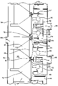
The interior of one embodiment of the process chamber 11 of the
apparatus 10 is illustrated schematically in Figures 7 and 16 and includes a
WO 95112007 ~ PCTIUS94/12380
I2
plurality of side-by-side coating devices 34. Each of these devices 34 is
provided
with at least one thin film deposition device which, in the preferred
embodiment, is a sputtering cathode 36. Preferably, each of the coating
devices 34
is provided with a pair of sputtering cathodes 36 and 39. The cathodes 36 and
39
are rotatable cathodes which are constructed of a target material and function
in
accordance with technology known in the art. During operation, each of the
cathodes 36 and 39 emits atoms or other small particles 40 for deposition onto
the
front screen 41 of a CRT 42 or other article to be coated.
Each of the coating devices 34 is defined in part by a pair of end
i o walls 44, the inner wall portions 45 including the cathode shielding wall
portions
46, and the outer side wall 32. The outer side wall 32 includes a port 49 for
evacuating gases from the chamber defining the interior of the coating devices
34
as described in greater detail below. In the system schematic of Figure 11,
each of
the evacuation ports 49 is connected with an evacuation or process zone pump
i5 50. Depending upon various factors, including the particular reactive gases
employed in each of the coating devices 34, it is possible for several of the
outlet
ports 49, or in some cases all of the ports 49, to be connected with a common
pump 50.
The plurality of coating devices 34 are positioned generally in line
2o and adjacent to one another to facilitate a continuous coating process.
During
operation, working or reactive gases are supplied to the sputtering cathodes
36
and 39 by means of a plurality of distribution manifolds 57. These manifolds
direct the working gases toward the magnetron cathodes 36 and 39, causing
emission or reaction of the particles 40 for deposition onto the CRT face 41.
WO 95112007 PCT/US94/12380
21~~~j8
13
Following bombardment of the cathodes 36 and 39, the working gases flow
through the openings 52 in the cathode shielding portions 46 and are then
evacuated through the evacuation port 49.
Positioned between the coating devices 34 and the front faces 41 of
the CRTs 42 and within the process chamber II is a deposition zone 33. The
deposition zone 33 is defined on one side by the coating devices 34 and on the
other side by the CRT screens 41 and the carrier barrier plates 6I. As will be
described in greater detail below, the barrier plates 61 of the carriers 58
cooperate
with adjacent carrier plates 6I and with the top and bottom walls 29 and 31 to
i o form a substantially continuous moving barrier extending throughout a
substantial portion of the length of the chamber I1.
Adjacent to the deposition zone 33 and positioned between the zone
33 and the side wall 30 is an isolation or exhaust zone or plenum 54. The zone
54
extends the entire length of the process section I1 (Figure 1) and is defined
on its
i 5 ends by the gate valves 16 and 26 and on its top and bottom by the top
wall 29 and
bottom wall 31 of the apparatus I0. One of its sides is defined by the side
wall 30,
while its other side is defined by various barrier plates 6I of the CRT
carriers.
The zone 54 is provided with a single outlet port 55 although multiple ports
can
be provided if desired. As illustrated in the schematic diagram of Figure 11,
a
2o separate exhaust pump or system 56 is connected with the port 55 for
generating
reduced pressure within the zone 54.
As illustrated best in Figures 2, 3 and 4, a CRT carrier 58 supports a
CRT 42. When used with the apparatus 10 of Figure 1, a plurality of carriers
58
transport the CRTs 42 past the coating devices 34 for coating. At the same
time,
WO 95!12007 ! r ~ .~ ~ PCTIUS94I12380
~1'~5~ ~~
14
the carriers 58, in conjunction with adjacent carriers and with portions of
the
apparatus 10, form a substantially continuous, moving barrier to substantially
isolate the deposition zone 33 from the exhaust zone 54 and thus the portions
of
the CRT 42 which are to remain uncoated. This substantially reduces or
s eliminates outgassing problems and facilitates the coating of CRT screens
following assembly. It also effectively reduces the deposition zone size of
the
process chamber I1 so that process parameters can be more accurately and
consistently controlled.
The carrier 58 includes a base 59 and a CRT support comprised of a
i o bottom 60, a pair of side brackets 62 and a front, generally rectangular
barrier
plate 61. The bottom 60 is connected with the base 59 by appropriate
connection
means. The brackets 62 are secured to the bottom 60 and to the rearward
surface
of the plate 6I by welding or the like to support the plate in a generally
vertical
orientation at right angles relative to the bottom 60. As illustrated best in
zs Figures 3 and 4, the barrier plate 6I is provided with a central opening 64
conforming substantially in size and configuration to a peripheral surface of
the
CRT 42. As shown in Figure 8, the rearward surface of the plate 6I is provided
with a plurality of standoffs 65 and threaded members 66 for connection with
tabs or ears 68 extending from the implosion band 69 of the CRT. With this
2o structure, the CRT 42 can be mounted relative to the barrier plate 6I with
the face
or screen 41 of the CRT 42 extending through the opening 64 and the remaining
portion of the CRT 42 extending to the rear of the plate 61. Preferably, the
barrier
plate 61 engages the implosion band 69 in a sealing relationship by an
elastomeric seal or the like so as to preclude passage of any outgas or other
CA 02175058 2004-08-04
material between the opening 64 and the CRT 42 or band 69. In some cases,
however, a small gap between the barrier 61 and the implosion band 69 can be
tolerated if the quantity or partial pressure vapors, etc. of gases passing
between
the exhaust zone 54 and the process zones 34 are insignificant in comparison
5 with the quantities or partial pressures of the reactive gases supplied to
the
sputter deposition process.
Positioned forwardly of the barrier plate 6I is a generally rectangular
mask or shield member 70 having a central opening 71 and top, bottom and side
edges. The member 70 is mounted in spaced relationship relative to the plate
61
to by a plurality of standoff members 73. In the preferred embodiment, the
central
opening 71 is generally aligned with the opening 64 of the plate 6I but is
larger as
illustrated best in Figures 3, 4, 5 and 8. Preferably, the shield member 70 is
spaced
forwardly from the barrier plate 61 a distance at least as great as the
distance
which the front face or screen 41 extends forwardly of the plate 61. A section
of
t5 Kapton film 74 may be provided between the opening 7I of the mask 70 and
the
opening 64 of the barrier 61 to improve the separation and the isolation of
the
front face 4I of the CRT from the exhaust zone 54. The film 74 is secured to
the
front face of the mask 70 by a plurality of tape strips 75. As shown best in
Figure
8, the film 74 extends inwardly from the opening 71 and then past the opening
zo 64. If needed or desired, the film 74 is retained relative to the barrier
plate 61 by a
plurality of tape strips (not shown). Preferably the film 74 is positioned
relative
to the front face 41 so that when the CRT is exposed to the deposition device,
the
coating extends over the entire front face 41 as well as a portion of the
implosion
band 69. Although provision of the film 74 is desirable, it is not necessary
as
.1 n 1 ~....r r! ..
WO 95112007 PCT/US94/12380
21'~~~r7~
16
shown in several of the alternate embodiments. Further, as shown in Figure 10,
the opening 7I in the mask member 70 may be smaller than the opening 64 if a
reduced portion of the front face 41 is desired to be coated.
Secured to one side of the barrier plate 6I is an overlapping edge tab
s 76 having an outer edge which is bent away from the plate 6I so as to
overlap the
plate 61 from an adjacent carrier as shown in Figure 6. As best shown in
Figure
16, the shield 70 should be positioned as close to the wall 45 and shield
portions
46 as possible. Further, the side edges of adjacent shield members 70 and
adjacent
barrier plates should be positioned as close together as possible. Minimizing
the
to gap between these surfaces not only maximizes the isolation and separation
between the exhaust and deposition zones 54 and 33, but, in the case of the
gap
between the shield 70 and the wall portions 45 and shield portions 46, also
minimizes the conductance or contamination between adjacent coating devices
34.
is Figures I5 and 17 illustrate an alternate embodiment for separating
the deposition and exhaust zones. In this alternate embodiment, the shield
member 70 of the embodiment of Figures 7 and 16 has been eliminated and
mating separation panel or barrier portions 83 are provided. T'he barrier
portions 83 (shown best in Figure 17) are connected with walls 29 and 3I and
2o extend along the entire length of the process section II. The portions 83
mate
with top and bottom edges of the barrier plate 61. In the preferred
embodiment,
the top and bottom edge of the plate 61 and portions 83 extend laterally to
improve separation between the deposition and exhaust zones. The side edges of
the barrier plates 6I of adjacent carriers in the embodiment of Figures 15 and
17
WO 95/12007
PCTIUS94/12380
I7
<'_~. q
should be positioned as close as possible to minimize the gap between them and
thus prevent, or at Least minimize, transmission of gases from the exhaust
zone 54 to the deposition zone 33. To further improve separation, an edge tab
76
may be provided between the barrier plate side edges of adjacent carriers 58.
Figure 12 illustrates a structure for obtaining improved separation
or isolation between adjacent coating devices 34. Such isolation may be
desirable
in cases where different working or reactive gases are used. In Figure 12, a
sealing roller 76 is mounted such that a portion extends through an opening in
the wall portion 78. By providing a shield or barrier 70 of sufficient length,
a seal
i o , is formed between the rollers 76 and the shield 70 as the CRTs 42 move
through
the apparatus. Such a structure effectively forms a seal, and thus prevents
the
flow of gases, etc., between adjacent coating devices 34.
Figure I3 is an illustration of an alternate apparatus for mounting
the CRT 42 relative to the carrier and for sealing the same relative to the
barrier
i s plate 61. In the embodiment of Figure 13, an elastomeric seal member 79
engages
a portion of the CRT 42 rearwardly of the implosion band 69. The CRT 42 is
supported relative to the barrier plate 6I by the threaded members 82 attached
to
peripheral ears 68 commonly provided around the CRT periphery. This
particular embodiment is preferred when outgassing contaminants resulting
2o from the implosion band 69 can be kept to a minimum. An advantage of this
particular embodiment is that the conductive coating applied to the front
screen
4I of the CRT 42 can extend up to and include a portion of the band 69,
thereby
insuring electrical contact between the conductive coating and the band 69 and
dissipating static electricity.
CA 02175058 2004-08-04 - . .
I8
Figure 14 illustrates a further embodiment for supporting the CRT
42 relative to the carrier and forming a seal between the barrier plate 61 and
a
peripheral edge of the CRT screen 41. In the embodiment of Figure 14, an
elastomeric seal 80 is positioned forward of the implosion band 69. An '
advantage of this embodiment is that it isolates the implosion band 69 from
the
deposition zone 34 and thus prevents or minimizes the band 69 as a source of
outgassing. The sealing force and CRT support in the embodiment of Figure 14
is provided by a yoke or rnllar 81 which is pressed against a rear surface
portion
of the CRT I1 by means of springs, etc. In all embodiments, however, a
io substantially continuous, moving barrier is formed in the process chamber
separating the exhaust and deposition zones.
Figures I8, 19 and 20 illustrate a further embodiment of a CRT
carrier. Specifically, as shown best in Figure I8, the carrier 85 includes a
base 86
and generally box-like structure comprising a top wall 88, a bottom wall 89
and a
pair of side walls 90, 9I. Joined with the walls 88-9I is a barrier plate 92
having a
pair of CRT receiving openings 94, 94. A CRT illustrated in phantom by the
reference character 95 is shown mounted within one of the openings 94. The
outside surface of the wall 90 is provided with an elongated seal or gasket
member 96 for sealing engagement with the exterior of the wall 91 of an
adjacent
2o carrier. Preferably, the seal 96 is constructed of silicon or Viton in
order to
minimize outgassing.
The bottom wall 89 is connected with a base 86 which includes
means on its bottom surface for engagement with the linear drive means of the
apparatus illustrated in Figure 1. The base 86 is provided with a counter
weight
* Trade Mark
WO 95/12007
PCT/US94112380
19
98 to provide stability to the carrier. Adjacent to the forward face of the
barrier
plate 92 is a mask 99 having a pair of openings 100, 100 aligned with the
opening
94, 94. The mask 99 is designed to be connected to the forward edges of the
walls
88-91 by a plurality of latch or other connection means 101. Preferably, the
mask
99 is spaced forwardly from the plate 92 a distance approximately equal to the
curvature of the CRT 95 which extends forward of the front surface of the
barrier
plate 92. A lower surface of the bottom wall 89 is provided with a lip I08
which
extends outwardly past the wall 9I for mating engagement with an adjacent
carrier as shown in Figure 20.
i o Figure 19 is a front elevational view of the carrier 85 with a
mounted CRT 95. As shown, means for mounting the CRT 95 to the plate 92
includes a plurality of support pins 102 adapted to extend through openings in
two of the mounting ears 105 of each CRT. Keepers or cotter pins I06 are then
inserted through openings in the pin ends to retain the ears 105 on the pins
102.
is A second pair of CRT mounting ears 105 are retained by pivotable latches
104.
As described above, a principal object of the present invention is to
provide an apparatus and method in which the deposition zone and the exhaust
zone are substantially isolated or separated from one another. This prevents
or
minimizes interference of the deposition process by outgasses from noncoated
2o portions of the article such as an assembled CRT. Substantial isolation or
separation of the deposition and exhaust zones in accordance with the present
invention can be accomplished in several ways. First by physically separating
the
two zones by minimizing the gaps between adjacent carrier side edges and
between top and bottom carrier edges and the process chamber walls, a partial
WO 95/12007 PCT/US94/12380
2~.~~~8
pressure differential between outgas gases and process gases across the
physical
barrier is created. A second way is by maintaining a total pressure
differential ,
between the deposition and exhaust zones so that prevailing movement of
gasses within the process chamber during operation is from the deposition zone
s to the exhaust zone; and third, by combining the physical separation with
the
maintenance of a pressure differential. The presence of the barrier also
functions
to confine the deposition zone, thereby facilitating control of the coating
process
parameters.
Physical separation can be maximized by sealing the barrier plate 61
i o to the article to be coated as shown in Figures 8 - I0, 13 and 14 and by
minimizing
the gaps between the side edges of adjacent carriers 58 and between the mating
top and bottom edges of carriers and barrier portions of the process chamber.
Small gaps can, however, be tolerated, particularly if combined with a
pressure
differential between the deposition and exhaust chambers. Preferably, gaps
i 5 between the barrier plate 61 and the CRT and between the carrier 58 and
mating
portions of the process chamber should be maintained at less than about 6 mm
and more preferably less than about 3 mm and most preferably less than about
1.5 mm. The size of the gap that can be tolerated, however, will depend on the
amount of pressure differential between the deposition and exhaust zones and
2o the proximity of the gap to the surface to be coated. A further factor
involves the
shape of the gap. For example, the movement of gases between zones can be
reduced by a serpentine shaped gap.
In the preferred embodiment, the deposition and exhaust zones 33
and 54 are provided with separate pumping systems, 50 and 56 (Figure 11)
WO 95/12007
PCT/US94/12380
21
respectively. The provision of separate pumping systems facilitates the
pressure
differential. In the preferred embodiment, the pressures in the deposition
zone 33 are maintained in the general range of about 1 x IO-3 to 8 x 10⁻³
Torr. In
the exhaust zone 54, pressures are preferably maintained in a general range of
s about 5 x 10⁻⁵ to
7 x 10-~ Torr. Preferably, the pressure differential between the zones is such
that
the deposition zone pressure exceeds the exhaust zone pressure by a factor of
at
least two and more preferably at least five.
Having described the structure of the present apparatus, the
io operation of the apparatus and the method of the present invention can be
understood best as follows.
First, in accordance with the method of the preferred embodiment,
a fully assembled CRT 42 is mounted to a CRT carrier 58 as illustrated in the
embodiment of Figures 2, 3 and 4 or any one of the various alternate
15 embodiments. For this purpose, the carrier may be a single CRT carrier 58
as
shown in Figures 2-6 or may be a double CRT carrier 58 as illustrated in the
schematic view of Figure 7 or the alternate carrier of Figure I8. In either
case, the
carrier is provided with a barrier plate having an opening substantially
conforming in size and configuration to a peripheral surface of the CRT 42. A
2o forwardly spaced mask or shield member 70 (Figures 7 and T6) or 99 (Figure
I8)
with openings may also be provided. Alternatively, the mask can be eliminated
as shown in the embodiment of Figures 15 and I7. In the embodiment of
Figures 7 and 16, a film 74 may optionally be provided between the openings 71
and 64 to improve isolation of the deposition zone 33 and the front face 41 of
the
WO 95/12007 . ~ PCT/ITS94/12380
~ ~. '~'~ ~ ~ S , v
22
CRT 42 from contaminating outgasses. Although it is desirable for the opening
64 in the barrier plate 61 to be sealed to a peripheral surface of the CRT 42,
a total
seal is not necessary. In fact, a small gap can be tolerated. Preferably,
however,
the partial pressures of gasses within the deposition zone 33 and the exhaust
zone 54 are such as to preclude migration of outgasses from the exhaust zone
54
into the deposition zone 33.
After the CRT 42 has been mounted to the CRT carrier, the gate
valve I6 (Figure 1) is closed and the air supply means 20 is actuated to
provide
the interior of the entry buffer chamber 12 with atmospheric pressure. The
i o door 15 is then opened and the carrier 58 with the attached CRT 42 is
positioned
within the entry buffer zone 12 as illustrated in Figures 5 and 6. In this
position,
the base 59 of the carrier 58 is positioned on the transport rollers 17. The
door I5
is then closed and latched and the air exhaust means 21 actuated to create
vacuum conditions within the chamber I2 substantially identical to those
within
i 5 the process chamber I I. The gate valve 16 is then raised and the carrier
with
mounted CRT 42 is transported into the process section 1I so that it abuts an
adjacent carrier. If desired, a dynamic seal between adjacent carriers as they
enter
and exit the process chamber I1 can be provided. If CRTs or other articles to
be
coated are not intended to be mounted in each carrier opening, dummy carriers
2o can be provided with glass inserts covering the CRT mounting openings. When
the carrier 58 and CRT 42 are positioned within the section lI, the gate valve
16
may be dosed, the chamber I2 brought to atmospheric pressure and a new carrier
and CRT introduced into the chamber 12 to repeat the cycle.
WO 95!12007 t~ -
PCT/US94/12380
23
If CRTs or other articles to be coated are not intended to be mounted
in each carrier opening, dummy carriers can be provided with glass inserts
covering the CRT mounting openings.
Within the section I1, the carrier 58 and CRT 42 are progressively
s moved along so that the front face 41 of the CRT is progressively moved past
the
various coating devices 34 within the deposition zone 33 for sequential
deposition of a thin film coating by the sputtering cathodes 36 and 39.
Because it
is possible and common for adjacent coating devices 34 to utilize different
working gasses, as well as different materials, it is preferable for each of
the
io devices 34 to be provided with separate evacuation pumps or pump systems 50
(Figure 11).
To minimize the contamination of working gasses and the like
from one coating apparatus 34 to another, it is preferable during movement of
the CRTs through the section I1 for the mask or shield portion 70 of the
i s carrier 58 to be positioned as close to the walls 45 and 46 as possible.
During the deposition process reduced pressure conditions are
maintained within the devices 34, and thus the deposition zone 33, by the
vacuum pumps 50 (Figure II) and in the exhaust zone 54 by the vacuum
pump 56 (Figure 11). Preferably, the pressure levels maintained in the
2o deposition zone 33 are slightly greater than that in the exhaust zone 54 so
that a
pressure differential is created. Thus, the prevailing movement of gases,
etc.,
although minimized, is from the deposition zone 33 to the exhaust zone 54.
In the above identified apparatus and method, to the extent
outgasses are released from electronic and other components of the assembled
WO 95!12007 PCT/L1S94/1238~
'~~.~5~8
24
CRT 42, they are isolated from the deposition process zone 33. Thus, such
outgasses are effectively prevented from interference with the deposition
process. This represents a significant advancement in the art and facilitates
the
thin film coating of an article such as a CRT screen after the CRT has been
s substantially assembled. Further, the maintenance of a moving barrier
through
the process zone effectively reduces the size of the deposition zone and
thereby
facilitates improved control of the process parameters. Still further, by
maintaining minimal gaps between the moving barrier and various wall
surfaces and portions of the chamber II and the devices 34, substantial
isolation
1 o between adjacent coating devices can be maintained.
Although the description of the preferred embodiment and method
have been quite specific, it is contemplated that various modifications could
be
made without deviating from the spirit of the present invention. Accordingly,
it
is intended that the scope of the present invention be dictated by the
appended
is claims rather than by the description of the preferred embodiment.