Note: Descriptions are shown in the official language in which they were submitted.
2 i 75276
MBT~OD AND ~YSTEM FOR A~O~ING AN INTEGRATED CIRCUIT
TO BF PORTABLY GENERATED FROH ONE MANUFACTURING
PPO~ TO ANOTHER
FIELD OF THE INVENTION
The present invention is directed toward generating
integrated circuits and more particularly to a system and
method for producing an integrated circuit that can be
portably produced regardless of the manufacturing process.
R~C~UND OF THE INVENTION
Integrated circuits are designed in a variety of fashions
for a variety of purposes. Initially, a custom cell or
megacell is designed which comprises a collection of gates and
transistors and interconnections therebetween.
For a conventional circuit, there is a preexisting
integrated circuit design environment including a schematic
capture station, a logic simulator, timing verifier, and
circuit simulator. The hardware of such design environments
generally minimally comprises a computer, keyboard, graphic
display means (such as a color graphic CRT display system),
and graphic input means (such as a mouse or a digitizing
tablet). Generally the hardware would be based upon a
commercially available computer workstation, such as those
provided by Sun Microsystems or by Apollo Computer
JAS 304 -1-
2 1 75276
Incorporated, and the software of the design environment would
be provided as an ~et of tools by one or more cadence
manufacturer, such as the design environments provided by
Mentor Graphics Incorporated. There also exists a logic
schematic prepared on the schematic capture station for which
an accurate logic simulation is desired, and from which a net-
list has been prepared. A net-list is a file comprising
descriptions of the logic primitives (e.g., AND/OR gates,
etc.) used in the logic schematic and the connectivity
therebetween. This is generally accomplished automatically by
the schematic capture system upon completion of the logic
schematic, although some systems may require an additional
step of logic compilation, whereby the user invokes a program
to perform the process of conversion of the graphical
schematic data to a net-list. In any case, the capability of
net-list generation is widely known and implemented in all
present schematic design environments.
Traditionally, the physical layout design is done with
physical layout tools, known generically as "polygon editor".
Experienced layout designers are employed to manually design
such integrated circuits with the sole objective of creating
a very area efficient design. One of the most important
constraints in a layout design is the process layout design
rules, which specify the spatial characteristics and limits of
éach process mask layer and the relationships between multiple
JAS 304 -2-
2175276
layers. These design rules are process technology specific.
The major drawbacks of the traditional approach in custom cell
(integrated circuit) design are (1) time consuming, (2) not
easily adaptable to new processes, and (3) very poor in terms
of logic/timing simulation capability.
In addition, it is not possible to provide an accurate
simulation model for such integrated circuits. Typically,
"behavioral model" is used to describe the functionality of
the cell. "Behavioral models" in great majority of cases do
not adequately model the cells' functional and timing
characteristics. Furthermore, there is often a need to have
the same custom cells in different "processes" (as in
fabrication), either to increase circuit performance, or to
have alternate sources for the product or to be integrated in
another design. Accordingly, what is needed is a system which
allows for the migration of a particular integrated circuit
portably from one process to another process quickly and
accurately. In addition, what is needed is a design
methodology that will allow for an integrated circuit design
to be used over and over again with only minor modifications
and within a variety of process environments. The present
invention addresses ~uch a need.
JAS 304 -3-
21 75276
8UMNARY OF THE INVENTION
A method and system for taking a first integrated circuit
from a first manufacturing process and generating a second
integrated circuit for a second manufacturing process is
disclosed. The method and system comprises providing a first
library from the first integrated circuit, the first library
defining the characteristics of the first gate array, and
mapping and characterizing the first library from the first
integrated circuit into a set of design criteria for the
second manufacturing process.
The method and system in accordance with the second
aspect also includes generating a plurality of a methodology
and system of databases representing libraries and information
about the design. The database will include the following
information: physical cell library, logic device library,
timing model library for the logic devices, design netlist and
physical connectivity of the logic devices. In addition, the
integrated circuit's physical size, functional behavior and
timing characteristics are fully defined by the above
database. The method and system in accordance with the
present invention also enables mapping of physical database to
allow for the recharacterizing of the timing models from one
IC fabrication process to any other IC fabrication process.
JAS 304 -~-
21 75276
~.
Accordingly through a system and method in accordance
with the present invention, an integrated circuit can be
portably manufactured on a plurality of different
manufacturing processes. The method and syætem therefore has
significant advantages over known conventional integrated
circuit design processes.
BRIEF D~P~PTPTION OF T~E DRA~ING~
Figure 1 is a diagram that shows the necessary required
design flow in this system for designing core integrated
circuit with a first manufacturing process.
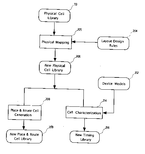
Figure 2 is a diagram that shows the creation of new
Physical, Place and Route, and Timing Libraries for an
integrated circuit when the integrated circuit is moved from
one process to another process.
Figure 3 is a diagram of the production of Physical
Database for a new integrated circuit utilizing the second
process after the creation of the particular libraries.
DE~TT~D DE8CRIPTION
The present invention is directed toward a system and
method for generating a design for an integrated circuit
regardless of the manufacturing process being utilized.
JAS 304 --~-
2 1 75276
.
The following description is presented to enable one of
ordinary skill in the art to make and use the invention as
provided in the context of a particular application and its
requirements. Various modifications to the preferred
embodiment will be readily apparent to those skilled in the
art, and the generic principles defined here may be applied to
other emho~iments. Thus, the present invention is not
intended to be limited to the embodiments shown, but is to be
accorded the widest scope consistent with the principles and
novel features disclosed herein.
In a conventional system for designing an integrated
circuit for integrated circuits, a logic designer would
prepare a schematic or a block diagram of the particular
integrated circuit and then would provide this block diagram
or schematic to an expert in layout design. The layout
designer would then utilize the schematic and a netlist
showing the different characteristics of the devices to be
used to design the layout of the circuit. This type of
methodology would oftentimes provide a efficiently organized
integrated circuit. However, such a system also consumes many
man hours of time for design.
one of the problems of the above identified methodology
is that for the design to be portable from one process to the
other, e.g, from an older fabrication process to a newer, more
advanced one, significant work on the part of the layout
JAS 304 -6-
2 1 75~76
designer is required. Typically the approach would be to
linearly scale down or "shrink" the different devices that are
part of the design. However, thiS is oftentimes not adequate
or practical because (1) not all the layout design rules
(constraints), i.e. "contact" size and "metal overlapping
contact amount" do not change by the same proportion, and (2)
not all the devices (therefore circuit parameters) change at
the same rate. That is, a resistor utilized in the integrated
circuit may change at one rate from one to another process
where a transistor in the same circuit may change at another
when manufacturing is transferring the manufacturing from one
process to another. In addition, through this conventional
process it is not possible to obtain an accurate simulation
model when moving from one process to another. Applicant,
through the present invention, has provided a method for being
able to move from process to process and still have accurate
information about the device.
To more specifically describe the features of the present
invention, a few terms will be defined. In the context of the
present application, "Netlist" means the connectivity
information of various logic elements of the integrated
circuit. The "Timing Library" for a specific integrated
circuit means the library of timing models speed, delay, etc.
of the corresponding "logic library". The "Logic Cell
Library" means the library of logic elements. The "Place and
JAS 304 -7-
2 ~ 75276
Route" database indicates a symbolic representation of the
physical connection of the devices. Finally, the "Physical
Cell Library" is the library which comprises of the actual
physical layers, or the different dimensions of the various
layers of the corresponding "Logic Library".
In a system and method in accordance with the present
invention once an integrated circuit is designed in one
process, the integrated circuit can be portably manufactured
on another process. To more particularly describe the
advantages and features of the present invention refer now to
Figures 1-3 which are diagrams showing the design for
generating an integrated circuit in accordance with the
present invention.
Figure 1 is a diagram that shows the necessary required
design flow in the construction of an integrated circuit.
Figure 2 is a diagram that shows the creation of new Physical,
Place and Route, and Timing Libraries for an integrated
circuit when the integrated circuit is moved from one process
to another process. Figure 3 is a diagram of the production
of Physical DatAh~se for a new integrated circuit utilizing
the second process after the creation of the particular
libraries.
Referring now to Figure 1, what is shown is a diagram of
the creation of the important portions of an integrated
circuit utilizing a first process. Initially, as is seen a
JAS 30~ -8-
2i 75276
.. .
design Netlist 102 is provided, along with the Timing Library
106 and the Logic Library 108 respectively to enable the Logic
Simulation 110. Next a Place and Route Cell Library 112 is
provided so that the final netlist (integrated circuit) can be
placed and routed 114. The end result of the place and route
step 114 is wiring information that allows the creation of the
integrated circuit 115 for the integrated circuit. The
integrated circuit includes the wiring information and the
physical information from the Physical Library 113 which after
incorporation or merging provides the physical information for
the integrated circuit. Accordingly, the integrated circuit
115, as is seen in Figure 1, comprises three different
databases 116-120. The Netlist Database 116 includes the
connectivity information providing a full logic description of
the integrated circuit. The Place and Route Database 118
describes all the physical connections of the integrated
circuit. The integrated circuit also includes the Physical
Database 120 which denotes all the physical layers of the
integrated circuit. This system can be fully automated,
therefore, given these databases, a new integrated circuit can
be provided which has all of the above characteristics.
Figure 2 is a diagram that shows the creation of new
libraries required for a new integrated circuit based upon
moving that integrated circuit to a different fabrication
process. In such a device, the Physical Library 113 from the
JAS 304 -9_
21 75276
.,~ .,
original manufacturing process along with the layout design
rules 204 are physically mapped 205 to produce a new Physical
Library 206. The prerequisite- for the methodology is the
built-in characteristics of the "Physical Library", which is,
unlike conventional "custom" cell library, typically more
structured, this lending itself to mapping easily with
computing software. This new Physical Cell Library 206 then
allows for generation of a new Place and Route Library 209 in
step 208. Device models 212 from the new process in
conjunction with the new Physical Cell Library 206 allow for
recharacterization of the cell library to create a new Timing
Library 216. The steps 208 and 214 can be done by computer
programs. Through the use of these three libraries 206, 209
and 216, as is seen, along with the other elements of the
process, the "building block" libraries of the new process are
ready to be used on the integrated circuit.
To more specifically describe this feature, refer now to
Figure 3. In this embodiment, the Logic Cell Library and the
new Timing Library 216 along with the design netlist 303
constitute the new circuit model of the integrated circuit
115. The Place and Route Database 118 from the original
integrated circuit 115, in conjunction with the new place and
route cell library, is mapped 302 into the new Place and Route
database 308. The mapping step 302 in this emboAiment can be
achieved with computer programs. It simply converts cell
JAS 304 -10-
21 75276
placements and interconnectivity wires from one coordinate
system to another. For example, the coordinate system for the
Place and Route DatAhi~s~ of the-first procesæ may have a grid
resolution of 1 microns in the x direction and 2 microns in
the y direction; in a second process, the grid resolution
could be 0.7 microns in the x direction and 1.2 micron in the
y direction, respectively. The new Place and Route Cell
Library 304 along with the new Place and Route DatAhAse 308
provide the necessary inputs to the physical datAhA~e
generation step 310. In this embodiment a new Physical
Database 312 is generated 310 from a new Physical Library 313.
In so doing, a completely new database (physical, place &
route and netlist) of the integrated circuit are created
(generated) for new manufacturing process. Furthermore, this
methodology can be applied hierarchically. In other words,
this integrated circuit can become a building block of a much
bigger, more complex integrated circuit. In this case, the
integrated circuit is a megacell (custom cell).
Through a system and meithod in accordance with the
present invention, firstly an integrated circuit is generated
essentially from the libraries associated with the integrated
circuit and the place and route information. In so doing, a
Netlist Database, a Place and Route Database and a Physical
Database can be generated therefrom that can be readily
implemented into a physical integrated circuit. In addition,
JAS 304 -11-
21 75276
when a new manufacturing process is utilized to generate a new
integrated circuit, the only things that need to be done are
a mapping of the physical cell library, generating new timing
models, and finally mapping of the Place and Route Database.
Accordingly, this system can be utilized for several different
processes across several different technologies to quickly
provide an integrated circuit for an integrated circuit.
Accordingly, through this process, a new integrated
circuit can be generated that is process independent, that
takes a minimal amount of time to design, and that does not
require as much modification after the new database is
generated.
Although the present invention has been described in
accordance with the embodiments shown, one of ordinary skill
in the art will readily recognize that there could be
variations to the embodiments and those variations would be
within the spirit and scope of the present invention. It
should be understood that the above-identified process would
have application to a gate array cell. That is, a gate array
cell manufactured on one process can be transferred to another
process utilizing the principles of the present invention.
Accordingly, many modifications may be made by one of ordinary
skill in the art without departing from the spirit and scope
of the appended claims.
JAS 304 -12-