Note: Descriptions are shown in the official language in which they were submitted.
2i 75861
POWER CONTROL METHOD AND APPARATUS SUITABLE
FOR USE IN A RADIO COMMUNICATION DEVICE
Field of the Invention
s
Generally, this invention relates to controlling power in
electronic equipment and, more specifically, to mAximi7.ing the
use of a battery's energy in a portable electronic device.
Background of the Invention
Traditionally, power control apparatus have been developed
to control power provided by a battery to a portable electronic
device. These power control apparatuses monitor the voltage of
- 15 the battery and compare the battery voltage to a hardware
undervoltage threshold. If the battery voltage falls below the
undervoltage threshold, then the power to the portable
electronic device is powered-off. Typically, this threshold is
positioned 200-300 millivolts above the lowest operating voltage
of the portable electronic device. In radio commlmic~tion
devices, the threshold was typically positioned 200-300
millivolts above the operating voltage of voltage regulators in
the radio communication device. The voltage regulators are
used to provide a steady ~efeIellce to the rest of the radio
commlmic~tion device. By providing such a threshold, the
radio communication device's operation was very reliable,
howt~v~r, some unused energy remained in the battery. The
amount of the unused energy differed dep~n~ling upon the type
of battery attached to the radio commlmic~tion device.
3 0 FIG. 1 is an illustration of a voltage/drain characteristic
100 of a NiCd (nickel cadmium) battery. As can be seen from
the voltage/drain characteristic, the amount of unused energy
rçm~inin~ in the battery after re~hing the traditional
undervoltage threshold 101 is minim~l FIG. 2 is an
3 5 illustration of a voltage/drain characteristic 200 of a lithium
., " 2l7s86l
ion battery. As can be seen from FIG. 2, the lithium ion battery
has a linear voltage/drain characteristic. Consequently, a
significant portion of unused energy rem~in-c in the battery
after re~ching the traditional undervoltage threshold 201. If a
5 lower undervoltage threshold could be provided, such as
threshold 203, then the operating time of the battery powered
equipment would be significantly increased.
In the portable electronic device market there is a push by
the manufaclulels to provide long lasting operation. This is
10 particularly true in the radio communication device market.
The introduction of lithium ion batteries is a significant
advance in battery te~hnology, offering increased operation
time of portable electronic devices. How~vel-, the impact of this
advance is not fully exploited with a traditional power control
l 5 apparatus, as described above. The traditional power control
apparatus powers-off the portable electronic device even though
there is a significant portion of unused energy rem~qining in
the battery. Thus, it would be advantageous to provide a power
control apparatus to utilize a larger portion of the energy in a
20 battery before powe~ g-off.
Brief Description of the Drawings
FIG. 1 is an illustration of a voltage/drain characteristic of
25 a NiCd battery as is known in the art.
FIG. 2 is an illustration of a voltage/drain characteristic of
a lithium ion battery as is known in the art.
FIG. 3 is an illustration in block diagram form of a radio
communication system including a portable radio
30 communication device which may be used in accordance with
the present invention.
FIG. 4 is an illustration in block diagram form of a power
control circuit of FIG. 3 in accordance with the present
lnvention.
2t75861
.
FIG. 5 is an illustration of a process flow chart in
accordance with the present invention.
Part 1 of FIG. 6 is an illustration of the performance of a
power control apparatus and is known in the prior art.
Part 2 of FIG. 6 is an illustration of the performance of a
power control apparatus in accordance with the present
nvention.
Detailed Description of a Preferred Embodiment
The present embotliment describes a portable radio
communication device for use in a radio communication
system. The radio commllnic~t.ion device is powered by a
rechargeable battery. The rechargeable battery is a lithium ion
l 5 battery. Ho~ ver, other batteries such as NiCd, nickel metal
hydride, and their equivalents could be used. The portable
radio commllnic~tion device includes power control circuitry
for monitoring the voltage level incominF from the battery and
provides power to the other electronic components, including
radio circuitry, contained within the radio communication
device.
The power control cilcuilly includes a boost regulator that
provides a constant level output voltage independent of the
input voltage, including input voltages which are less than the
oul~ l, regulated voltage. The boosted regulator out~lll signal
is used to generate an internal refe~ellce signal for use
throughout the radio communication device, including an
analog to digital collvel ler (ADC) for digitizing the battery
voltage for use by the power control ~ .;uill y. The digitized
3 0 battery voltage is compared to at least one threshold and in
response to the comparison, the radio communication device is
put into a powered-off state in one of many known manners,
such as that described in U.S. Patent No. 4,642,479, issued on
February 10, 1987 and ~ ne~l to the ~-~si~nee of the present
3 5 invention. Using the boost regulator o~ ul signal as a
2 1 7586 1
reference to the ADC allows the battery voltage to fall below the
voltage of the internal lere,e~,ce signal and shutoff at a lower
undervoltage threshold than the traditional undervoltage
threshold described in the background of the invention. Using
this lower undervoltage threshold m~ximi7es the ~mount of
battery energy used from the battery.
Additionally, a hardware comparator is used to compare
the battery voltage to a second battery voltage threshold and a
third battery voltage threshold, thereby ~ v~llting ll~m~e of
l 0 the battery and radio communication device circuitry.
Specifically, when the radio commllnic~tion device is in a
powered-up state, the battery voltage is comp~red to a first
hardware undervoltage threshold that is less than the software
undervoltage threshold. When the radio communication
l 5 device is in a powered-off state, the battery voltage is compared
to a second hardware undervoltage threshold that is greater
than the software undervoltage threshold. The first hardware
undervoltage threshold protects the battery from harm when
the software power control cil~ y fails. The second
hardware undervoltage threshold ensures proper operation of
the radio communication device during advancement to the
powered-up state. Upon arrival at the powered-up state, the
hardware undervoltage threshold switches to the first
hardware undervoltage threshold.
FIG. 3 is an illustration in block diagram form of a radio
communication system 300. The radio communication system
300 includes a fixed site transceiver 301. The fixed site
transceiver 301 sends and receives radio frequency (RF) sign~
to and from multiple radio commllnis~tion devices within a
fixed geographic area. One such radio communication device
is radio communication device 303 of FIG. 3. The RF sign~
transmitted between the fixed site transceiver 301 and the radio
communication device 303 provide radio commlmic~tion
services such as radio telephone service, electronic mail
service, wireless fax service, and short message service. Other
21 7586~
.
equally sufficient embodiments of the present invention may
include other combinations of these communication services as
well as other known radio commlmic~t.ion services.
The radio commllnic~tion device 303, also referred to as a
portable electronic device 303, includes an antenna 305, a
transmitter 307, a receiver 309, a processor 311, an user
interface 313, a power control circuit, also lefelled to as a
power control apparatus 315, and a battery 317. The radio
communication device 303 receives the RF siEn~l~ through the
1 0 antenna 305. The ~ntqnn~ 305 col~vel ~ the received RF signAl.
into electrical RF æign~ for use by the leceiver 309. The
receiver 309 demodulates the electrical RF ,siEn~l~ and recovers
the data transmitted using the RF ,si~n~l~. Additionally, the
radio receiver 309 outputs the data to the processor 311. The
l 5 processor 311 includes at least a main mi~;lo~locessor, such as
an MC 68040 available from Motorola, Inc., and associated
memory, as well as, other control cil~;uits including integrated
~;ilCuitS and other known technologies. The processor 311
formats the received data output from the radio receiver 309
into recogni~hle voice or mesg~ging information for use by
other parts of the radio device circuitry including the user
interface 313. The user interface 313 communicates the
formatted data output to the user via a speaker, display, and
any other medium of communication.
Upon tr~n.~mi.~ion of RF sign~ from the radio
communication device 303 to the fixed site transceiver 301, the
user interface 313 transmits user input data to the processor
311. Such data may include voice data and or mes.s~EinE
information. The processor 311 formats the informzltion
obtained from the user interface 313 and transmits the
formatted information to the radio transmitter 307. The radio
transmitter 307 converts the formatted information into
electrical RF-modulated .~ign~l~ and oull~uls these to the
antenna 305 for tr~n.~mi.~ion to the fixed site transceiver 301.
2 1 7586 1
In the l~lefel,ad embodiment, the battery 317 is of a lithium
ion type. Although other batteries such as nickel cadmium
and nickel metal hydride and any other known battery type
may be substituted, it is believed that this invention is most
beneficial to those portable electronic devices which use linear
discharge-type batteries, such as lithium ion batteries. The
battery 317 oul~uls a ground signal and a positive battery
oul~ signal (B+). The B+ signal has a battery voltage that is
monitored by the power control cil~;uilly 315. In the ~fefelled
1 0 embodiment, the power control cirC li~ly 315 monitors or
compares the voltage of the B+ signal to three independent
threshold sign~ . The first threshold is a software shutdown
voltage threshold. In order to be compared, the B+ signal is
digitized using an ADC that uses an internal lefe~e"ce
l S generated by a boost regulator. Using the boost regulator
allows the software undervoltage threshold to be at the lowest
operating point of the radio communication device and lower
than the traditional hardware undervoltage threshold. As
previously discussed, the traditional hardware undervoltage
2 0 was set 200-300 millivolts above the regulator operating point.
This traditional threshold was required because once the
battery fell below the voltage of the regulated output the voltage
of a non-boosted lefelellce would fall with the voltage of the
battery. Thus, in the traditional system, if this lower software
undervoltage threshold shutdown was employed, the
traditional system would never in(lic:lte a shut off condition.
Lowelillg the threshold for shutoffwhen the radio
communication device is in the powered-up state allows use of
the unused energy in the battery that could not be used with the
traditional hardware undervoltage circuit. This allows the
radio communication device 303 to increase its operation time
significantly over those phones av~ qhle in the prior art.
Additionally, the power control cil~;uilly 315 includes a
hardware comparison with two additional hardware
undervoltage thresholds. While the radio communication
21 75361
device 303 i8 in the poweled-up state, the voltage of the B+
signal is compared to a first hardware undervoltage threshold
that is lower than the software undervoltage threshold. In the
~lefelled embodiment, the first hardware undervoltage
S threshold is set equal to 2.7 volts.
While the portable radio communication device is in the
~o~ve~ed-off state, the voltage of the B+ signal is compared to a
second hardware undervoltage threshold that is higher than
the software undervoltage threshold. In the preferred
l 0 embodiment, the second hardware undervoltage threshold is
set equal to 3.1 volts. The second hardware undervoltage
threshold is set to a level that pr.dv~llts the radio
commllnic~tion device 303 from powe~ g up in an illegal state
and ensures operation in the powered-up state of the radio
l 5 communication device for a reasonable amount of time.
Details of the power control cilc~ 315 are illustrated in FIG.
4.
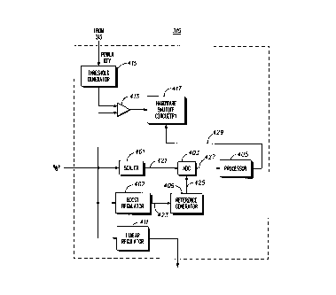
FIG. 4 is an illustration in block diagram form of the power
control CilCuilly 315 of FIG. 3. In the ~lefelled embodiment,
the power control cilcuill ~ 315 includes a scaler 401, an
~n~log-to-digital converter 403 (ADC), a processor 405, a boost
regulator 407, a lefelellce generator 409, a linear regulator
411, a hardware comparator 413, a threshold generator 415,
and a hardware shutoff .;ir~ ill y 417.
While the radio communication device 303 is in the
powered-up state, the voltage on the B+ signal 321 is input into
scaler 401. The scaler 401 is not a necessary part of the present
invention, but it is preferred. Scaler 401 scales the voltage on
the B+ signal 321 to optimally fit an input voltage range of the
3 0 ADC 403. Additionally, the B+ signal 321 is input into the boost
regulator 407, the linear regulator 411, and the hardware
comp~rator 413. The boost regulator 407 may be a boost
regulator model MAX 631 available from lV~xim Integrated
Products. The function of the boost is to provide an oull u~
voltage that is higher than its input voltage. Although the
21 7586 1
power control circuit 315 only includes one linear regulator
411, the actual number of linear regulators used in a radio
commllnicAt.ion device will vary depen~lin~ upon the specific
needs of the design of the particular radio communication
device. The linear regulator 411 is used to provide a regulated
voltage to a portion of the radio communication device circuitry
included in the radio communication device 303. The proper
operation of the linear regulator 411 requires a voltage on the
B+ signal at least 0.2 volts higher than the ouL~u~ voltage of the
l 0 linear regulator 411.
The regulator output signal 423 of the boost regulator 407
carries a boosted regulator voltage and is input into the
refe,e,llce generator 409. In the prefelled embodiment the
l~fe~ ce generator 409 is used to control variations in the
boosted regulator output signal 423 and provide a steady
internal lefelellce signal 425 to the ADC 403 as well as other
;uill ~ within the radio communication device 303. The
,~fe~llce generator 409 is not an essenti~l element of the
present invention. It is merely a tool by which a smooth
lefe~ellce is provided in the ~lefel,ed embodiment. Other
equally sufficient means, including an improved boost
regulator, may be substituted for the lefelence generator 409.
The ADC 403 lltili7.es the ~efer~lce signal to sample the
voltage of the B+ signal and generate a digitized battery voltage
signal 427. The digitized battery voltage signal 427 is input into
the processor 405. The processor 405 may share .;il.;uil, ~ with
the processor 311 of FIG. 3, or it may be a stand alone
proces.~ing circuit, depçn-ling upon the implementation of the
invention. In the pl2felled embodiment the processor 405
3 0 includes a memory device for providing storage of a computer
program as well as a microprocessor for executing the steps of
the computer program. Details concerning the computer
program stored on the computer memory device are illustrated
in process flow chart form in FIG. 5. Generally, the digitized
battery voltage signal 427 is coInp~red to a predetermined
21 75861
software undervoltage threshold while the radio
communication device is in the powered-up state. If the
digitized battery voltage falls below the predetermined software
undervoltage threshold, then the radio commllnic~tion device
5 is powered-off in one of many known manners. One such
m~nner is described in U.S. Patent No. 4,642,479, issued on
February 10, 1987 and ~igne~ to the ~ nee of the present
invçntion- Once the software shutdown is completed, the
processor 405 oul~uls a power-off signal 429 that is input to the
10 hardware shutoffcil~;uilly 417. The hardware shutoff
cilcuiLly removes power to the rem~ining radio
communication device ~ ;Uitly.
If the soIlwa~ e shutdown procedure fails to execute due to
an unforeseen event, a backup hardware shutdown is provided
15 in the ~lefelled embo~liment of the power control cil~;uilly 315.
Specifically, the threshold generator 415 oul~ul~ a first
haldwale undervoltage threshold to the comparator 413. The
battery voltage, B+, is input to the comr~rator 413 and
compared to the first hardware undervoltage threshold. If the
20 battery voltage B+ falls below the first hardware undervoltage
threshold, then the comparator 413 oul~uls a power-off signal
to the hardware shutoff~ ;uilly 417. The hardware shutoff
circuitry 417 removes power to the rem~ining radio
communication device circuitry. In the preferred
25 embodiment, the first hardware undervoltage threshold is set
equal to 2.7 volts, which is lower than the software
undervoltage threshold. Using a hardware shut down circuit
as a fail safe or secondary method of power shut down
increases the reli~qhility of the power control cil~uilly 315.
3 0 Because the hardware used to shut down the radio
communication device can operate at significantly lower
voltages than the software controlled shut down, the hardware
shut down circuitry ensures that the battery and the radio
communication device 303 will be shut down properly.
- ` 21 7586~
10 -
Additionally, the preferred embodiment includes a second
hardware undervoltage threshold for comparing the battery
voltage B+ thereto when the radio communication device is in a
powered-off state. Specifically, when a power key of the radio
communication device, located in the user interface 313 of FIG.
3, is depressed by a user to power-on the radio communication
device 303, the battery voltage, B+, is comp~red, at the
comparator 413, to a second hardware undervoltage threshold
generated by the threshold generator 415. If the battery voltage
l 0 B+ exceeds the second hardware undervoltage threshold, then
the rem~ining radio commllnic~tion device circuitry is
powered-up in a known m~nner. After normal power-up
procedures are completed, the threshold generator 415 oul~uts
the first hardware undervoltage threshold to the comparator
l 5 413. The battery voltage B+ continues to be comp~red at
comparator 413 to one of the thresholds generated by the
threshold generator 415, as described above. In the preferred
embodiment, the first hardware undervoltage threshold is less
than the second hardware undervoltage threshold.
Specifically, the second hardware undervoltage threshold is set
equal to 3.1 volts and the first hardware undervoltage threshold
is set equal to 2.7 volts. Setting the second hallwale
undervoltage threshold equal to 3.1 volts prevents the radio
communication device from powering-up in an illegal state.
This ensures that upon power-up of the radio communication
device 303, all the components contained within the radio
commllnis~tion device 303 will properly operate for a sufficient
length of time so as not to be a nlli~nce to the user of the radio
communication device 303.
FIG. 5 is an illustration of a process flow chart of the
program contained in a memory within the processor 405 in
FIG. 5. At block 501, the program provides a digital battery
voltage and a software undervoltage threshold. At decision
block 503, the program compares the digitized battery voltage
3 5 B+ to the software undervoltage threshold. If the battery
; ~ 2 1 7586 ~
voltage is greater than the software undervoltage threshold,
then the program continues to provide power to the reIn~ining
c;l-;.~illy in the radio commlmic~t.ion device-303, at block 505.
If the digitized battery voltage B+ is less than the software
undervoltage threshold, then the program powers down the
radio communication device 303 at function block 507.
Typically, the power-off function as indicated in function block
507 sends a signal from the radio commllnic~tion device 303 to
the fixed site transce*er 301 in~lic~ting that it is ~n~ling any
communication including communications now in progress
with the fixed site transceiv~r and requests an acknowledge to
be returned to the radio communication device 303. Next, the
radio commlmic~tion device 303 waits a predetermined
amount of time until an acknowledge signal is returned from
l S the fixed site transceiver 301. After leceivil,g the acknowledge
~ign~l, the function block 507 sends the power-off signal 429
from the processor 405 to the hardware shutoff-;ilcuilly 417.
The hardware shutoff circuitry 417 provides a me~h~ni.~m for
discontinuing power to the rem~ining cil~uilly in the radio
communication device 303.
Part 1 of FIG. 6 is an illustration of various undervoltage
thresholds and related thresholds available in the prior art.
An axis 601 is the intlic~tion of battery voltage of a battery
available in the prior art with volts varying between 0 and 6
volts. The following thresholds are indicated in part 1 of FIG.
6: a software undervoltage threshold is equal to 5.15 volts as
indicated at 603; a hardware undervoltage threshold in the
prior art is set equal to 5.05 volts as in~ te~l at 605; and the
voltage regulator thresholds within the radio communication
3 0 device are at 4.75 volts as indicated at 607. Thus, in the prior
art the software undervoltage threshold and the hardware
undervoltage threshold were both set significantly higher than
the operating voltage of the voltage regulators of the radio
communication device, as illustrated in Part 1 of FIG. 6~
2175861
'~
12
Part 2 of FIG. 6 is an illustration of various undervoltage
thresholds and related thresholds in the preferred
embodiment. Here an axis 609 is an indication of battery
voltage of the battery 317 of FIG.3. The battery voltage
S in~licP~te-l in 609 varies between 0 and 7 volts. The following
thresholds are in~lic~ted in part 2 of FIG. 6: a software
undervoltage threshold is set equal to 2.8 volts as indicated at
lafe~el,ce numeral 613; a nomin~l voltage regulator threshold
for the voltage regulators contained within the radio
l 0 commllnicA~;on device 303 operates safely at 2.75 volts as
indicated at ~efe~ellce numeral 615; a firæt hardware
undervoltage threshold is set equal to 2.7 volts as indicated at
617; and a second hardware undervoltage threshold is set equal
to 3.1 volts as indicated at reference numeral 611. The internal
l 5 reference signal generated at the output of the reference
generator 409 is set equal to 2.66 volts as in~ic~t~l by reference
numeral 619. Thus, the present invention, as indicated in Part
2 of FIG. 6, allows the battery voltage, B+, to tli~ h~rge as low
as 2.7 volts before shutting off the radio communication device
303. 2.7 volts is chosen to ensure that the hardware shutoff,
including any tolerances, does not encroach upon the software
shutoff, thus, ensuring an orderly shutdown sequence.
Consequently, the power control ci~cuill y 315 e~t~n~ the
operation time of the radio commlmic~tion device 303 by
allowing the battery voltage to tlicch~rge further than the
power control ~ ;uill~ previously avAil.qhle. Additionally, the
second hardware undervoltage threshold as indicated at 611
insures proper power-up of the radio communication device
303.