Note: Descriptions are shown in the official language in which they were submitted.
CA 02175943 2001-07-30
~~'~~943
SQUEAK AND DELETION RESISTANT
IMAGING MEMBER AND SYSTEM
BACKGROUND OFTHE INVENTION
This invention relates in general to xerography and more
specifically to an imaging member comprising a novel charge transport
layer. The invention further relates to a novel electrophotographic system
containing a cleaning blade, particularly a doctor blade.
In recent years, interest has been shown in electrophotographic
drums for use in high speed office copying machines. Some of these drums
are multilayered devices comprising a conductive substrate layer, a
blocking interface layer, an optional adhesive layer, a charge generation
layer and a charge transport layer. The charge transport layer comprises an
organic charge transport molecule dissolved in a polymeric matrix
material. This layer is substantially nonabsorbing in the spectral region of
intended use, e.g., visible light, but is "active" in that it allows (1)
injection
of photogenerated holes from the charge generation lacer and (2)
efficient transport of these charges to the surface of the transport layer to
discharge a surface charge thereon.
One class of charge transport molecules, N,N'-Biphenyl-N,N'-
bis(alkylphenyl)-[1,1'-biphenyl]-4,4'-diamines, has been extensively studied
in the forms of solutions or dispersions in polycarbonate polymers. The
conductivity of this class of compounds in polycarbonate polymers has
been found to increase under certain circumstances. When imaging
members employing this class of compounds have a residual amount of a
halogen-containing alkane solvent in the transport layer and they are
subjected to ultraviolet radiation, a condition known as "cycle down"
progressively develops as the device is cycled in the xerographic process:
"Cycle down" refers to the progressive increase in conductivity of the
transport layer such that in a relatively short period of time the charge
acceptance of the device deteriorates.
Also, special precautions have to be taken with regard to the
handling of the devices employing these compounds. They cannot be
stored or left exposed to ambient room light for any length of time
because fluorescent lamps employed in most buildings contain a UV
component. This UV radiation causes devices left- exposed to the room
light to undergo gradual deterioration resulting in an increase in the
CA 02175943 2001-07-30
~r . 2~'~5~43
_2_
conductivity of the transport layer. Chemical stabilization of the physical
properties of polymers has been well pursued and additives are available
that stabilize various polymers against ultraviolet induced discoloration or
ultraviolet induced mechanical failures.
A photoreceptor is also subjected to a large number of chemical
species produced by the charging devices typically used. A number of
these species, especially the oxides of nitrogen, can react with hole
transporting materials. This results in an electrially conductive surface. An
electrostatic image residing on such a surface tends to spread, and in
severe cases can totally desperse, producing a fuzzy to non-existant final
image. By chemical stabilization, as used in the present invention, is meant
the elimination or minimization of chemically induced conductive species
on the surface of the photoreceptor.
To be useful as a stabilizer in a cyclic duplicating machine, the
additive, in addition to preventing chemical degradation, has to meet
another stringent requirement. The additive should not introduce traps,
or conductive species of its own. Even a small number of traps results in
the cumulative trapping phenomenon generally referred to as "cycle up."
The trap could be an isolated electronic state of the additive or it could
result from the additive changing the character of the dispersion of the
host molecule in the binder matrix. The generation of conductive species
on the photoreceptor surface would result in unacceptable image quality.
This conductive species could be the oxidized state of the hole transporting
moiety present in the photoreceptor transport layer.
It has been found that when some multi-layered drum imaging
members are cleaned with flexible cleaning blades, the cleaning blade
interacts with the drum imaging members in such a way as to cause a
vibration in the drum. This vibration may be perceived as an irritating
squeak. This squeak can be eliminated by plasticizing the charge transport
layer. However, plasticization of the charge transport layer softens the
layer and adversely affects its durability. In other words, the layer,
subjected to the abrasive conditions generated by the interaction of the
development materials and processes, tends to wear out too rapidly. Also,
high loading of plasticizers may adversely affect the electrical mobility of
the imaging member and interfere with other eaectrical and physical
properties.
CA 02175943 2001-07-30
2115943
a ' , ' - -
U.S. Patent No. 4,297,425, to Pai et al., discloses an imaging
member containing a hole transport layer comprising a poiycarbonate
resinous material having a residual amount of a halogen-containing
organic solvent. Dispersed in the layer is a diamine as a charge transport
compound and a diary) or triaryl methane compound as a stabilizing
compound to overcome effects of the residual halogen-containing solvent.
The reference discloses a weight ratio of the stabilizing compound to the
diamine compound of from 0.0005:1 to 0.7:1.
However, U.S. Patent No. 4,297,425 does not disclose any
relationship of the diary) or triaryl methane compound to squeaking in a
drum imaging member cleaned using a cleaning blade. The reference does
not teach the use of diary) or triaryl methane compounds in amounts
greater than 0.1:1 relative to the diamine compound or selecting an
electrophotographic system comprising a cleaning blade and a drum
imaging member with a transport layer containing a diary) or triaryl
methane compound. It also does not teach an imaging member having a
transport layer free from halogen containing solvents comprising a diary)
ortriaryl methane compound.
SUMMARY OF THE INVENTION
An aspect of the present invention provides an electrophotographic
system comprising a cleaning blade, preferably a doctor blade, and an
imaging member, particularly a drum, comprising a charge generation layer
and a charge transport layer comprising a diamine compound of the class
defined below and a diary) or triaryl methane compound of the class defined
below.
An aspect of the present invention further provides an imaging
member comprising a charge generation layer and a charge transport layer
comprising a diamine compound of the class defined below and a diary) or
triaryl methane compound, wherein the weight ratio of the methane
compound to the diamine compound is preferably greater than 0.1:1.
An aspect of the present invention further provides an imaging
member comprising a charge generation layer and a charge transport layer
comprising a diamine compound of the class defined below and a diary) or
triaryl methane compound of the class defined below, wherein the transport
layer is free of halogen containing organic solvent.
It has been found that the addition to the transport layer of the diary)
or triaryl methane compound significant reduces or eliminates
CA 02175943 2001-07-30
2115943
-4-
chemical reactions leading to the deleterious effect of image blurring due to
lateral conductivity on the photoreceptor surface. Further, the addition to
the
transport layer of diaryl or triaryl methane compound significantly reduces
the
squeak problem when a drum imaging member is cleaned using a cleaning
blade. The use of this class of additives has no apparent deleterious effects
on the physical or electrical properties of the charge transport layer.
Further aspects of the invention are as follows:
An electrophotographic imaging system comprising:
(a) an imaging member drum comprising a charge generation layer and a
contiguous charge transport layer, said charge transport layer comprising:
(1) a diamine compound of formula (I):
(1)
wherein R is
X X
or -CI-iZ
and wherein X is independently selected from the group consisting of alkyl
having from 1 to
about 4 carbon atoms and chlorine in the ortho, meta or para position, and
;n.. ,;:,
%._
CA 02175943 2001-07-30
217543
- 4a -
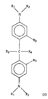
(2) a methane compound of formula (II):
R
y
N
R3
Rs C Ra
R3
N
R~ RZ
(II)
wherein R, and RZ are independently selected from the group consisting of
alkyl having 1 to 8
carbon atoms, aryl, alkaryl and aralkyl, where said aryl is a phenyl group or
a condensed ring
group, and where the alkyl group of said alkaryl and aralkyl has 1 to 4 carbon
atoms;
R3 and R4 are independently selected from the group consisting of hydrogen
and CH3; and
RS is selected from the group consisting of alkyl having 1 to 8 carbon atoms,
aryl, alkaryl, aralkyl, and disubstituted aminophenyl group having
substituents independently
selected from the group consisting of alkyl having 1 to 8 carbon atoms, aryl,
alkaryl and aralkyl,
where each said aryl is a phenyl group or a condensed ring group, and each
said alkyl group of
each said alkaryl and aralkyl has 1 to 4 carbon atoms; and
(b) a cleaning blade that comes into contact with the charge transport layer.
CA 02175943 2001-07-30
2175943
- 4b -
An imaging member comprising a charge generation layer and a contiguous
charge transport layer, said charge transport layer comprising:
( I ) a diamine compound of formula (I):
Q~ ~ o ~~
(I)
wherein R is
X X
or -CHZ
and wherein X is independently selected from the group consisting of alkyl
having from I to
about 4 carbon atoms and chlorine in the ortho, meta or para position, and
(2) a compound of formula (II):
CA 02175943 2001-07-30
2175943
-4c-
R~\ /RZ
N
R3
R5 C R4
0
N
Rt RZ
(II)
wherein R, and Rz are independently selected from the group consisting of
alkyl having 1 to 8
carbon atoms, aryl, alkaryl and aralkyl, where said aryl is a phenyl group or
a condensed ring
group, and where the alkyl group of said alkaryl and aralkyl has 1 to 4 carbon
atoms;
R3 and R4 are independently selected from the group consisting of hydrogen and
CH3; and
RS is selected from the group consisting of alkyl having 1 to 8 carbon atoms,
aryl,
alkaryl, aralkyl, and disubstituted aminophenyl group having substituents
independently
selected from the group consisting of alkyl having 1 to 8 carbon atoms, aryl,
alkaryl and aralkyl,
where each said aryl is a phenyl group or a condensed ring group, and each
said alkyl group of
each said alkaryl and aralkyl has 1 to 4 carbon atoms,
wherein a weight ratio of said compound of formula (II) to said diamine
compound
of formula (I) is from greater than 0.1:1 to 1:1.
~:.:w~a
CA 02175943 2001-07-30
. 2115943
- 4d -
An imaging member comprising a charge generation layer and a contiguous
charge transport layer, said charge transport layer comprising:
(1) a diamine compound of formula (I):
°~a,~ o o ~~°
(I)
wherein R is
X X
or -CHZ
and wherein X is independently selected from the group consisting of alkyl
having from 1 to
about 4 carbon atoms and chlorine in the ortho, meta or para position, and
(2) a compound of formula (II):
A
CA 02175943 2001-07-30
2175943
- ...~..
' - 4e -
R
N
R3
Rs C Ro
w o
N
(II)
wherein R, and RZ are independently selected from the group consisting of
alkyl having 1 to 8
carbon atoms, aryl, alkaryl and arallcyl, where said aryl is a phenyl group or
a condensed ring
group, and where the alkyl group of said alkaryl and aralkyl has 1 to 4 carbon
atoms;
R~ and R4 are independently selected from the group consisting of hydrogen and
CI-i3; and
Rs is selected from the group consisting of alkyl having 1 to 8 carbon atoms,
aryl,
alkaryl, aralkyl, and disubstituted aminophenyl group having substituents
independently
selected from the group consisting of alkyl having 1 to 8 carbon atoms, aryl,
alkaryI and aralkyl,
where each said aryl is a phenyl group or a condensed ring group, and each
said alkyl group of
each said alkaryl and aralkyl has 1 to 4 carbon atoms,
wherein a weight ratio of said compound of formula (II) to said diamine
compound
of formula (I) is from 0.04:1 to 1:1;
said transport layer being free of halogen-containing organic solvent.
CA 02175943 2001-07-30
2175943
-4f-
BRIEF DESCRIPTION OF THE DRAWING
FIGURE 1 is a schematic illustration of an embodiment of the
instant invention, which comprises an imaging member having a charge
generation layer overcoated with a charge transport layer.
FIGURE 2 is an illustration of a drum imaging member and a
cleaning blade.
FIGURE 3 is a side view of FIGURE 2.
DETAILED DESCRIPTION OF PREFERRED EMBODIMENTS
Referring to FIGURE 1, reference character 30 designates an
imaging member that comprises a supporting substrate 11, a charge
generation layer 12, and a charge transport layer 15.
Substrate 11 is preferably comprised of any conductive material.
Typical conductors comprise aluminum, steel, nickel, brass or the like. The
substrate may be rigid or flexible and of any convenient thickness. In a
preferred embodiment, the substrate is a drum. In addition, other typical
substrates include flexible belts or sleeves, sheets, webs, plates and
cylinders. The substrate or support may also comprise a composite
structure such as a thin conductive coating contained on a paper base; a
plastic coated with a thin conductive layer such as aluminum, nickel or
copper iodide; or glass coated with a thin conductive coating of chromium
or tin oxide.
In a preferred embodiment, the imaging member further
contains a blocking layer 14 between the substrate 11 and the charge
generation layer 12. Charge blocking layer 14 may be any charge blocking
layer known to one of ordinary skill in the art. In a more preferred
embodiment, the charge blocking layer comprises an alcohol soluble
polyamide.
In an embodiment, the imaging member further comprises an
adhesive layer to adhere the charge generation layer 12 to the substrate.
CA 02175943 2001-07-30
2175943
-5-
Charge generation layer 12 generally contains photoconductive
particles dispersed in binder.
Binder material may comprise any electrically insulating resin
such as those disclosed in Middleton el al., U.S. Pat. No. 3,121,006. Specific
examples include, but are not limited to, polystyrene, acrylic and
methacrylic ester polymers, polyvinyl carbazole, polyvinylchlorides,
mixtures thereof and the like.
When using an electrically inactive or insulating resin, there
should be particle-to-particle contact between the photoconductive
particles. In this case, the photoconductive particles are preferably present
in an amount of at least about 10% by volume of the binder layer, with no
limit on the maximum amount of particles in the binder layer. if the matrix
or binder comprises an active material, e.g., polyvinyl carbazole, the
photoconductive particles need only comprise about 1 % or less by volume
of the binder layer with no limitation on the maximum amount of particles
in the binder layer. The thickness of generation layer 72 is not critical and
any suitable thickness may be selected so long as the objects of the
invention are achieved. For example, layerthicknesses from about 0.05 to
about 40 microns have been found to be satisfactory.
The photoconductive particles may be any material capable of
photogenerating holes and injecting photogenerated holes into the
contiguous charge transport layer 15. Any suitable inorganic or organic
photoconductor, and mixtures thereof, may be employed. Inorganic
materials include inorganic crystalline photoconductive compounds and
inorganic photoconductive glasses. Typical inorganic compounds include,
but are not limited to, cadmium sulfoselenide, cadmium selenide,
cadmium sulfide, mixtures thereof and the like. Typical inorganic
photoconductive glasses include, but are not limited to, amorphous
selenium, selenium alloys such as selenium-tellurium, selenium-tellurium-
arsenic, seleniumarsenic, mixtures thereof and the like. Selenium may also
be used in a crystalline form known as trigonal selenium.
Typical organic photoconductive particles that may be used as
charge generators in embodiments also include, but are not limited to,
phthalocyanine pigment such as the X-form of metal free phthalocyanine
described in U.S. Pat. No. 3,357,989 to Byrne et al; metal phthalocyanines
such as copper or vanadyl phthalocyanine; quinacridones such as those
CA 02175943 2001-07-30
2175943
-6-
available from duPont under the tradename Monastral Red, Monastral
Violet and Monastral Red Y; substituted 2,4-diamino-triazines disclosed in
U.S. Pat. No. 3,445,227 to Weinberger; triphenodioxazines disclosed in U.S.
Pat. No. 3,442,781 to Weinberger; polynuclear aromatic quinones such as
those available from Allied Chemical Corporation under the tradename
Indo Double Scarlet, lndofast Violet Lake B, Indofast Brilliant Scarlet and
Indofast Orange; mixtures thereof and the like. The photoconductive
particles may be present in the charge generation layer in an amount from
about 0.5% to about 95% by volume.
Preferably, the photoconductive particles are sensitive to
infrared light. More preferably, the photoconductive particles are infrared
sensitive phthalocyanine pigments, such and vanadyl phthalocyanine.
It is to be understood that the charge generation layer need not
be a binder resin having dispersed photoconductive particles. In
embodiments, the charge generation layer can be a homogeneous layer,
such as amorphous selenium, selenium alloys such as selenium-tellurium-
arsenic alloys and, in fact, any other charge generating photoconductive
material. For flexible imaging members, the charge generating material
should be selected to withstand a minimum flexing stress required in a
flexible imaging member.
Transport layer 15 generally comprises a transparent electrically
inactive polycarbonate resinous material having dispersed therein from
about 25 to about 75% by weight of the composition of one or more of the
diamines within the scope of formula (1):
°~a,~ o o ~,a~° ,~~
wherein R is
CA 02175943 2001-07-30
~1'~~ ~4~
. _, _
X X
or --CHz
and wherein X is independently selected from the group consisting of an
alkyl group having from 1 to about 4 carbon atoms (e.g. methyl, ethyl,
propyl, butyl, etc.) and chlorine in the ortho, meta or para position.
A preferred diamine charge transport material is N,N'-diphenyl-
N,N'-bis(3-methyl-phenyl)-[1,1'-biphenyl]-4;4'-d famine.
In general, the thickness of transport layer 15 is from about 5 to
about 100 microns, but thicknesses outside this range can also be used.
Preferred polycarbonate resins for the transport layer have a
molecular weight from about 20,000 to about 120,000, more. preferably
from about 50,000 to about 120,000. Exemplary electrically inactive
resinous materials are poly(4,4'-isopropyiidenediphenylene) carbonate and
poly(4,4'-cyclohexylidenediphenylene) carbonate. Preferably, the charge
transport layer contains from about 40 to about 60% polycarbonate
resinous material.
Transport layer 15, as described above, is substantially
nonabsorbing to light in the wavelength region employed to generate
holes in the photoconductive layer. A preferred range for xerographic
utility is from about 4,000 to about 8,000 angstrom units. In addition, the
photoconductor should be responsive to all wavelengths from 4,000 to
8,000 angstrom units it panchromatic responses are required.
Photoconductor-active material combinations of the instant invention
result in the injection and subsequent transport of holes across the physical
interface between the photoconductor and the active material.
In order to effectively dissolve the charge transport diamine
compound in a polycarbonate matrix, a suitable mutual solvent system
may be employed. Methylene chloride, i.e. CH2C12, is effective in
embodiments for this purpose, although other halogen-containing
solvents such as chloroform, and 1,2-dichloroethane.and the like, and non-
halogen-containing organic solvents such as tetrahydrofuran and the like
CA 02175943 2001-07-30
217543
_$_
can be employed. Mixtures of these and other solvents may also suitably
be employed in embodiments of the invention.
The transport layer may also comprise a residual amount of the
above solvent. As used herein, a "residual amount" of a solvent represents
from about 0.01 to about 1.0 weight percent of the transport layer.
Subjecting the transport layer to a temperature of about 80°C for
about 2
hours will generally reduce the solvent content to about 0.1 weight
percent.
Dispersed or dissolved in the transport layer, in order to greatly
minimize or eliminate both corona induced image deletion and cleaning
blade squeak, is one or more of the diaryl or triaryi urethanes within the
scope of formula (III:
CA 02175943 2001-07-30
217594
_g_
R1~ ~R2
N
R5 C R4
R3
N
R1
wherein R~ and R2 are independently selected from the group consisting of
an alkyl having 1 to 8 carbon atoms, aryl, alkaryl and aralkyl, where said
aryl is a phenyl group or a condensed ring group, and where the alkyl
group of said alkaryl and aralkyl has 1 to 4 carbon atoms; R3 and R4 are
independently selected from the group consisting of hydrogen and CH3;
and RS is selected from the group consisting of an alkyl having 1 to 8
carbon atoms, aryl, alkaryl, aralkyl, and disubstituted aminophenyl group
having substituents independently selected from the group consisting of
an alkyl having 1 to 8 carbon atoms, aryl, alkaryl and aralkyl, where each
said aryl is a phenyl group or a condensed ring group, and each said alkyl
group of each said alkaryi and aralkyl has i to 4 carbon atoms. 1n a
preferred embodiment, R4 is hydrogen.
Examples of compounds of this class include, but are not limited
to, bis(4-N,N'-diethylamino-2-methylphenyi)phenyi~ methane and bis-[4-
N,N'-diethylamino-2-chlorophenyl] phenyl methane. A preferred
CA 02175943 2001-07-30
10-
compound in embodiments of this invention is bis(4-N,N'-diethylamino-2-
methylphenyl) phenyl methane.
The compound of formula (ll) may be employed in any effective
amount that will inhibit or greatly minimize the deleterious effects of UV
light on the charge transport diamine compound and/or the squeak.
Generally, the compound of formula (II) is present in a weight ratio to the
diamine transport compound of formula (I) of no more than 1:1.
Preferably, the compound of formula (II) is present in a weight ratio to the
diamine transport compound of greater than 0.7 :1 and less than 1:1. More
preferably, the weight ratio is between greater than 0.1:1 and about 0.5:1.
Even more preferably the weight ratio is from about 0.012:1 to about
0.25:1.
The electrophotographic system of the present invention, in
embodiments, further comprises a cleaning blade, as demonstrated in
FIGURES 2 and 3. Referring to FIGURES 2 and 3, reference character 30
designates a drum imaging member and reference character 40 designates
a cleaning blade.
Typical cleaning blades are utilized in the doctor mode, which
scrapes residual toner particles from the imaging surface. Typical cleaning
blade materials, include, for example, polyurethane, polyesterurethane,
and polyetherurethane.
The following examples further specifically define the present
invention with respect to preparing the imaging member. The
percentages are by weight unless otherwise indicated. The examples are
intended to illustrate various comparisons and embodiments of the instant
invention. It is understood that the invention is not limited to the
materials, conditions, process parameters, etc. recited therein.
COMPARATIVE EXAMPLE I
A Charge generation layer is prepared on a 84 mm diameter
aluminum drum as follows: 2.4 grams polyvinyl butryal is dissolved in 36.6
gram butylacetate. To this solution are added 1.3 grams of vanadyl
phthalocyanine and the solution is then ball milled for about 48 hours. The
resulting slurry is diluted with 52.2 grams butylacetate. An approximately
0.5 to 1.0 micron thick layer is applied from a coating of this slurry onto a
substrate that has been previously coated with a thin alcohol soluble
polyamide. This layer is heated at 105°C for 10 minutes in a forced air
oven.
An approximately 25 micron thick transport layer is formed on
top of the charge generation layer as follows:
CA 02175943 2001-07-30
21'~594~
_11_
2.4 grams of poly(4,4'-cyclohexylidenediphenylene) carbonate
and 1.6 gram of N,N'-diphenyl-N,N'-bis(3-methylphenyl)-[1,1'-biphenyl]-
4,4'-diamine in about 20 grams of chlorobenzene. A layer of this
combination is deposited onto the charge generation layer so that after
the removal of solvent at 120°C for 1.0 hour an approximate 20-25
micron
thick layer remains.
When xerographically tested, some evidence of image deletion
is noted when the photoreceptor is subjected to the corotron parking
deletion test at 80°F180% RH. The test procedure allows the charge
corotron and the photoreceptor main drives to run continuously for an
hour. The apparatus was shutdown and allowed to stand for ten minutes.
After this period, five test prints were made, and inspected for evidence of
parking deletions. Five test prints were again generated an hour later, and
again approximately 16 hours later. In addition squeak measurements
taken at various temperatures exhibited some unacceptable results as
shown in Table 1
TAB LE 1
(C) Running
55.. 1
50 5
45 5
40 5
3S 3
30 2
25 2
Squeak grades 1-best; 5-worst
1-2 acceptable, 3-5 unacceptabe
To examine the squeak produced by the device, the drum
imaging member is cleaned using a polyurethane type doctor blade.
Although the doctor blade is effective in removing the residual image, an
irritating squeak is emitted.
CA 02175943 2001-07-30
21'~ ~ 943
- 12-
EXAMPLE l
A charge generation layer composed of vanadyl phthalocyanine
and polyvinyl butryal is prepared on a drum in the same manner as
Comparative Example 1. A transport layer is prepared from a solution of
8.6 grams of poly(4,4'-cyciohexyiidenediphenylene) carbonate, 5.2 grams
of N,N'-Biphenyl-N,N'-bis(3-methyiphenyl)-[1,1'-biphenyl]-4,4'-diamine
and 0.6 gram of bis(4'-N,N'-diethylamino-2-methylphenyl) phenyl methane
in 45.6 grams of chlorobenzene. A layer of this combination is deposited
onto the charge generation layer so that after removal of the
chlorobenzene solvent an approximately 20-25 micron thick layer remains.
The device is heated at 120°C for about 1 hour in vacuum.
When electrically and xerographically tested, there is no increase
in dark decay, and no image deletion probelms are noted at 80°F/80% RH.
The degradation of the diamine containing layer is prevented by the
addition of the substituted methane molecule. Further, the squeak
measurements at various temperatures are demonstrated in Tale 2.
TABLE 2
SQUEAK TESTING
____ -"
C Startua Runni~n Shutdown .
.~......
55 1 1
50 1 1 1
45 1 1 2
40 1 1 1
35 1 1 1
30 ~ 1 _
25 1 1
~queaK graces are rated from 1 (best) to 5 (worst), 1-2 being acceptable, 3-
being unacceptable.
EXAMPLE ll
A photoreceptor is prepared similar to the device of Example I
except that the transport layer composition is varied slightly. The transport
layer is coated from a solution of 8.6 grams of poly(4,4'-
cyclohexylidenediphenyiene) carbonate, 5.5 grams of the diamine and 0.3
gram of the substituted methane compound in 45.6 grams chlorobenzene.
CA 02175943 2001-07-30
~~.'~~~43
-13-
After deposition of the transport layer, the device is heated at
120°C for 1
hour.
When electrically tested, no change in dark decay and no
increase in residual potential is observed. The photodischarge of the
device containing the diamine and the substituted methane compound in
polycarbonate is the same as that of the device containing no substituted
methane compound. The presence of the substituted methane compound
does not adversely impact the charge transport characteristics of the
transport layer. Further, the squeak grades are acceptable, as
demonstrated in Tabie 3.
TABLE 3
SQUEAK TESTING
.__ ~ -_.
C Startup Runnin Shutdown
55 1 4 1
50 1 1
45 1 1 2
40 1 1
35 1 1
30 1 ~ ~
~ 25
5queaK grades are rated 1-5: 1-2 being acceptable, 3-5 being
unacceptable.