Note: Descriptions are shown in the official language in which they were submitted.
~ WO96/08801 2 1 7 6 1 3 5 PCT~Sg5/12159
DESCRIPTION
DATA LINK MODULE FOR TIME DIVISION
MULTIPLEXING CONTROL SYSTEMS
FIELD OF THE lNv~ lON:
This invention relates generally to the field of control
systems and, more particularly, to control systems using data
link modules communicating on a serial time division multiplex
bus.
DESCRIPTION OF THE ~FT-~n ART INCLUDING lN~-O ~TION DISCLOSED
UNDER 37 C.F.R. 1.97-199:
Control systems employing a serial multiplex bus for
controlling at least one output device by a plurality of input
devices are well ]cnown. Some known control systems use
software protocols, operating under the direction of a
computer, in which all control signal data is conveyed in
multi-bit bytes or in packets of multi-bit bytes. Examples of
such software protocol control systems are the LonWorks local
operating network by Echelon Company of Palo Alto, California;
the home automation system Consumer Electronics Bus (CEbus) by
the Electronic Industry Association, the Controller Area
Network (CAN) by Robert Bosch, GmbH of Stuttgart, Germany and
the World Factory Implementation Protocol by the WorldFIP
Committee of Research Triangle Park, North Carolina. Known
software protocol control systems dlsadvantageously require
multi-bit bytes, typically 16-bit bytes, for conveying only one
bit of data. Although software protocol control systems are
designed to convey multi-bit bytes or words, they are
disadvantageously 10 - 100 times slower than hardware protocol
systems, such as the invention, in conveying multibit words.
In most software protocol control systems, the control protocol
is composed of a header, the number of words in the
WO96/08801 ~ 7 6 1 3 5 PCT~S9S/12159
transmission, load identi~ication, load status and checksum.
In most such systems, a minimum of six 8-bit words are needed
to turn on one load. In some software protocol systems, up to
three times as many bits are required.
Software protocol systems have their communication
capabilities disadvantageously centralized, or lumped, in a
computer that uses software to operate the control system; they
disadvantageously require the computer in order to function,
and therefore, if the computer malfunctions, then the control
system will malfunction.
Other serial multiplex control systems use single bits of
data to convey control signals and such systems have their
communication capabilities distributed throughout the
system,usually at each input and output location. Most of
these distributed, single-bit systems have hardware protocols
without any programmabillty. An example of this type of
single-bit, hardware protocol control system is the Actuator
Sensor Interface (ASI) by ASI Verein eV Geschaftsfuhrung of
Odenthal, Germany. Other examples are shown and described in
U.S. Patent Nos. 4,052,566 and 4,052,567 issued October 4, 1977
to MacKay; U.S. Patent No. 4,156,112 issued May 22, 1979 to
Moreland; U.S. Patent No. 4,435,706 issued March 6, 1984 to
Callan; and U.S. Patent No. 4,682,168 issued July 21, 1987 to
Chang, et al.
Hardware protocol systems are known to use a programmable
logic controller (PLC) which is a computer programmed in ladder
logic. Such systems disadvantageously require multiple lengthy
cable runs interconnecting the input and output devices to a
terminal. The execution speed of a PLC computer is often too
slow to provide real time operation.
` Most known single-bit, hardware protocol systems are not
programmable; however, an example of one such system that is
~ WO96/08801 2 1 7 6 1 3 5 pcT~s9sll2ls9
programmable, through firmware, is described in U.S. Patent No.
4,808,994 issued February 28, 1989 to Riley. Known
programmable systems, such as that of the aforesaid patent of
Riley require additional dedicated terminals on the module for
acceptance of programming information.
Known single-bit, hardware protocol control systems, such
as that of the aforementioned patent of Riley, multiplex frames
of time which are further divided into 256 time slots, each
time slot representing an address and each input and output
device being associated with an address The above described
single-bit, hardware protocol systems are relatively simple
compared to the software protocol systems, and they lack the
capability to directly handle multi-bit words of data. The
control system of the aforementioned patent of Riley can
directly handle at most 2-bit words. Single-bit hardware
protocol control systems disadvantageously require modification
by complicated additional circuitry to convey multi-bit words
of data. However, the complicated additional circuitry
disadvantageously restricts known modified single-bit hardware
protocol systems to a fixed word length. In the prior art two
channel data link modules of the aforementioned patent of
Riley, the beginning address of a multi-bit word is determined
by the address of one of the channels, but disadvantageously,
the ending address of the multi-bit word is not selectable.
The ending address is disadvantageously fixed at either eight
bits after the beginning address if a host computer is used, or
at sixteen bits after the beginning address if no host computer
is used.
The complicated additional circuitry used with known data
link modules is mounted external to a main integrated circuit
on the data link module. In the aforementioned patént~of
Riley, the additional circuitry generates, during a part of the
PCT/US95/121 !59
WO 96/08801 2 1 7 6 ~ 3 ~
PAGE 4 MISSING
~ WO96/08801 2 1 76 1 35 PCT~S95/12159
described complicated additional circuitry takes up substantial
space in known data link modules.
Known data link module integrated circuits have a
transistor internal to the integrated circuit for driving the
data bus voltage low in order to represent a signal in negative
logic. Known data bus currents are about thirty milliamperes,
and known data bus voltages are about twelve volts. However,
the internal transistor used for driving the data bus low in
known data link module integrated circuits often fails when the
data bus current and voltage becomes slightly higher than
normal, such as fifty milliamperes and sixteen volts.
Control systems are used in environments such as
manufacturing and assembly factories and are exposed to
electromagnetic noise, static, and spikes, pulses and transient
voltages (herein referred to collectively as "noise"). Known
data link modules passively rely upon the lack of temporal
coincidence between noise and signals to avoid noise
interference. The presence of noise can cause an output device
to respond at an inappropriate moment or fail to respond when
the output device should do so. Solely relying upon data
signals being synchronized with an edge of a clock pulse has
been found insufficient to sufficiently eliminate the effect of
noise on a control system.
Known data link modules have a relatively narrow operating
voltage range, usually nine to thirteen volts, and it is
impossible to use known data link modules with both twelve volt
and the popular 24 volt systems without adding additional
circuitry external to the integrated circuit for conversion of
voltages.
Propagation delays and certain other conditions can
- produce a false output signal under certain conditions during
start-up which are preferably avoided. The known systems
WO96/08801 2 f 7 6 ~ 3 5 PCT~S95/121S9
respond to changes in an input signal occurring within a time-
slot to produce false outputs. Known data link modules also
continue to produce an output signal even after a loss of a
master clock signal which reduces the degree of control during
such condi~ions.
The prior art data link module of the aforementioned
patent of Riley has a third output that is a logical
combination of the two other outputs. The polarity of the
other two outputs is selectable, but disadvantageously the
polarity of the third output is not selectable independently of
the polarity of the other two outputs, and as a result,
sophisticated logic functions cannot be easily implemented.
Known hardware protocol, serial multiplex control systems
lack circuitry to determine whether the data bus is open, or
lacks continuity. Such known control systems merely check
whether the data bus is shorted. Furthermore, known data link
modules lack circuitry for selectively checking the continuity
of a line connecting an individual module to the data bus and
for selectively turning off a module in the event the data line
to that module has faulted. Known control systems use the
clock module to place a test pulse on the data bus during the
sync period. Then, the circuitry on known clock modules
determines whether the attempt at placing a test pulse on the
data bus succeeded. If the attempt at placing the test pulse
on the data bus failed, known control systems merely turn off
the master clock; however, merely turning off the master clock
does not immediately prevent output modules from continuing to
produce false control signals to output devices. Furthermore,
known control systems disadvantageously test the condition of
the data bus only at the clock module. The test performed by
the clock module on known control systems does not, and can
not, determine whether a data line to an individual data link
WO96/0880l . . ~ PCT~s95ll2ls9
7 6 ~ 3 5
module is intact because known data link modules lack
additional circuitry for receipt of the test pulse.
.
SUMMARY OF THE lNv~L~lON
It is therefore the principal object of the present
invention to provide a data link module for use in a time
division multiplexing control system which overcomes the
various disadvantages of the known data link module.
This object is achieved in part by provision of a data
link module with means for producing output control signals in
response to input signals received on a data bus input terminal
on a time division basis during an associated one of a
plurality of time division multiplexing time slots, the
improvement being an input signal conditioner with means for
initiating generation of an intermediate data pulse in response
to the signals at the data bus input terminal exceeding a pulse
initiation threshold voltage, means for terminating generation
of the intermediate data pulse in response to the signals at
the data bus input decreasing beneath a pulse termination
threshold voltage different from the pulse initiation threshold
voltage, an intermediate pulse continuity checker for
determining whether the intermediate data pulse is extant at
each of a plurality of occurrences of the address time slot
associated with the data link module and means responsive to
the pulse continuity checker for producing a conditioned input
signal only when it is determined that the intermediate data
pulse is extant during each of said plurality of address time
slots.
The object is also achieved by providing a data link
module powered by a DC supply voltage with means for producing
an output control signal in response to data received on a data
bus on a time di~ision multiplexing basis for use in a time
WO96/08801 2 ~ 7 6 ~ ~ ~ PCT~S95112159
division multiplexing control system having a master clock for
producing a master clock signal, the improvement being a power
on reset delay having means for detecting the application of DC
supply voltage to the data link module and means for inhibiting
the control signal producing means from changing the output
control signal in response to data prior to the continuous
application of the DC supply voltage for a preselected time
period.
Further, the object is achieved in part by provision of a
data link module with a local input terminal to be applied to
an input circuit and means for generating an output signal
responsive to input signals applied to the input circuit on a
time division multiplexing basis, the improvement being a
safety input protection circuit having means for detecting a
selected one of a plurality of different conditions of the data
link module and means responsive to said condition detecting
means to inhibit the input circuit from responding to changes
in the input signals at the input terminal.
Moreover, object of the present invention is achieved by
providing a data link module with an integrated circuit having
means for producing a data output signal representative of a
data bus signal on a time division multiplexing basis for use
in a time division multiplexing control system having a master
synchronous clock for producing a master clock signal for
establishing time division multiplexing frames, a clock loss
output lock having means for detecting loss of the clock signal
and means for inhibiting said output signal producing means
from changing the state of the output signal despite changes in
the data bus signal in response to detecting loss of the master
clock signal.
Also, the object is obtained by provision of a data link
module with an input terminal for receipt of local input
~ WO96/08801 ~ 2 1 76 1 ~ PcT~s9gl2ls9
control signals and means for generating output control signals
in response to the local input signals, the improvement being a
safety output protection circuit having means for sensing at
least one condition of the data link module and means
responsive to the condition sensing means to inhibit the output
control signal generating means from changing output signals in
response to the changes in the input signals while said at
least one condition is being sensed.
Obtainment of the object is achieved in part by providing
a data link module for use in a control system with a master
clock signal and in which a plurality of the data link modules
are interconnected on a data bus to selectively convey control
signals from input devices connected to some of the data link
modules to output devices connected to others of the data link
modules on a time division multiplexing basis in which
successive frames of time are divided into a plurality of time
slots, the improvement being a data verifier having means
responsive to the master clock signal for successively storing
the data appearing on the bus during a selected time slot for
each of a selected plural number of frames, means responsive to
the data storing means for verifying the repetitive occurrence
of the same data during the selected time slot for each of the
plurality of frames and means responsive to the verifying means
for producing an output signal representative of the data only
in response to the data being verified.
Yet further, the object of the invention is obtained in
part by providing a data link module with a data bus input
terminal for receipt of control data on a time division
multiplexing basis and conveying that data to at least two
primary output terminals, each primary output terminal having
an associated polarity, and a logic circuit for producing a
combinational output signal based on a preselected logical
WO96/08801 ~ 7 6 1 3 5 PCT~S9S/l2159
combination of the data conveyed to at least two inputs of the
logic circuit from the at least two primary output terminals,
the improvement being a polarity selector circuit with means
for storing an input polarity selection for each input to the
logic circuit and means for controlling the polarity of each
input to the logic circuit in accordance with the polarity
selection independently of the polarities of the primary output
terminals.
Also achieving the object is provision of a data link
module for the passage of a local input signal at an input
terminal during a preselected associated one of a plurality of
time division multiplexing time slots defined by a synchronous
master clock signal to a data bus terminal, the improvement
being an input synchronizer with means responsive to the
synchronous master clock signal and the input signal to store
the input signal occurring at the beginning of the associated
one of the plurality of time division multiplexing time slots
for substantially the entire duration of the associated time
slot regardless of subsequent changes in the local input signal
during the associated time slot and means for passing the
stored input signal to a data bus terminal during substantially
the entire duration of the associated time slot.
The object is also achieved in the preferred embodiment by
providing a data link module for operation in a time division
multiplex control system selectively in one of first and second
modes of operation, the improvement being a mode selection
indicator having means responsive to the selecting means for
producing a mode selection signal indicating which of the first
and second modes has been selected and means responsive to the
mode selection signal to automatically provide data onto a data
bus at different times during at least one address associated
with the data link module depending upon the mode selected.
WO96/08801 ~ 7 6 ~ 3 5 pcT~s9sll2lss
11
Moreover, the object of the present invention is obtained
by provision of a data link module having an integrated circuit
with means for generating a plural number of multiplexing time
slots per frame in synchronization with a master clock, the
improvement being a multiplexing frame identifier having means
on the integrated circuit for counting the number of time slots
in each frame of the master clock in response to the time slots
generating means, means on the integrated circuit responsive to
the counting means for decoding an address of the master clock
and means responsive to the decoding means for providing a
multiplex address clock output signal on the data link module
during a preselected portion of each frame of the master clock.
The object of the invention is further achieved by
provision of a data link module for use in a time division
multiplexing control system with input terminals for connection
with ~ DC supply, a system clock signal and a data bus for time
division multiplexed digital communication with other data link
modules, the improvement being a module programmer having means
for storing a program for the module, means responsive to a
preselected variation from normal operating parameters of at
least one of input terminals for the DC supply and system clock
signal to enable the program storing means to receive
programming data from the data bus.
Also, the object of the invention is obtained by providing
a data link module with means for conveying input data signals
at an input terminal to a data bus during a preselected
associated one of a plurality of time division multiplex
addresses definable by cycles of a master synchronous clock
connectable to a clock input terminal, the improvement being an
input word extender having means for storing a selected one of
the plurality of addresses as a start address, means for
selecting another one of the addresses independently of the
WO96/08801 - ~ 7 6 ~ 3 5 PCT~S9S1121S9
- 12
selected one of the plurality of addresses, means for storing
the other selected one of the plurality of addresses as a stop
address selected independently of the start address, means for
generating a shift clock out signal in synchronization with the
master synchronous clock to identify a plurality of addresses
between said stored start address and said independently
selected stored stop address during the time between occurrence
of the start address and the stop address when an input data
signal is produced and means responsive to the shift clock out
signal to cause the input data signal conveying means to convey
input data signals to the data bus terminal during each of the
addresses between the start and stop address.
Obtainment of the object of the invention is achieved by a
data link module with means for conveying data at a data bus
terminal to an output terminal during a preselectable
associated one of a plurality of time division multiplex
addresses definable by the cycles of a master synchronous clock
connectable to a clock input terminal, the improvement being an
output word extender having means for storing a start address,
means for storing a stop address, means for generating a shift
clock in signal in synchronization with the master synchronous
clock to identify a plurality of addresses between the start
and stop addresses during the time between occurrence of the
start address and stop address and means responsive to the
shift clock in signal to cause the input data conveying means
to convey data on the data bus to the output terminal during
each of the addresses between the start and stop addresses.
Also achieving the object is provision of a data ink
module with an integrated circuit with an data bus terminal for
receipt of digital data signals from a data bus, a local input
terminal for receipt of input signals from a local lnput
device, and a time division multiplexing address defining one
~ WO96/08801 ~ 2 ~ 7 6 1 3 5 pcT~s95ll2lss
13
of a plurality of time slots between synchronization pulses, a
high voltage protection circuit having a switchable breakdown
device with an input junction and a pair of transconductive
outputs and having a breakdown voltage at which a short is
created between the transconductive outputs, means for
connecting one of the transconductive outputs to a data bus
susceptible to voltage spikes in excess of the breakdown
voltage and detrimental to the integrated circuit if applied to
the input, means for connecting the other transconductive
output to a reference potential and means responsive to the
address and to the signals at at least one of the local input
terminal and the data bus terminal to provide a drive signal to
the input junction of the switchable breakdown device to
provide an appropriate data signal on the data bus during the
time slot of the address of the data link module, said
switchable breakdown device breaking down to protect the
integrated circuit from said voltage spikes when not being
driven to provide data signals to the data bus.
Moreover, the object of the present invention is obtained
by providing a data link module with an integrated circuit with
a direct current supply input terminal for receiving a direct
current voltage between voltage levels V1 and V2, where V1 < V2
and circuitry for passing signal data through a data link
module in accordance with program information stored in a
program storage element, the improvement being a program
enabler having means on the integrated circuit for activating
the signal passing circuitry when the direct current supply
voltage is between voltage levels V1 and V3, said means on the
integrated circuit also activating the signal passing circuitry
when the direct current supply voltage is between voltage
levels V4 and V2, where V1 < V3 < V4 < V2 and means responsive to
the DC supply voltage between voltage levels V3 and V4 for
WO96/08801 ~ t 76 1 35 PCT~Sgsll2lss
14
enabling the program storage element to accept new program
information.
Still further, the object of the invention is achieved by
provision of a data link module including circuitry for passing
local voltage inputs at an input terminal to a data bus on a
time division multiplexing basis, the improvement being a local
input voltage range selector having means for selecting one of
a plurality of different input voltage levels acceptable for
handling by the data link module, means responsive to the
selecting means for storing a selected input voltage level and
means responsive to the storing means for operating circuitry
of the data link module in accordance with the stored voltage
level selection.
Yet further, the object of the invention is obtained by
providing a data link module for receiving data signals from a
data bus in a time division serial multiplex control system
with a master clock module for sending a test signal over the
data bus, the improvement being a data bus integrity checker
having means responsive to the test signal connected to the
data bus for determining whether the data bus is intact and
means responsive to the determining means for permitting
receipt by the data link module of data signals from the data
bus.
BRIEF DESCRIPTION OF THE DRAWINGS
The foregoing objects and advantageous features of the
invention will be explained in greater detail and others will
be made apparent from the detailed description of the preferred
embodiment of the present invention which is given with
reference to the several figures of the drawing, in which:
~WO96/08801 2 1 7 6 1 3 5 P~S9~12159
Fig. 1 is a simplified schematic diagram of a control
system using preferred embodiments of data link modules of the
present invention;
Figs. 2A and 2B form a composite functional block diagram
of the ci~cuit of a preferred embodiment of a data link module
integrated circuit which form part of the Output Modules and
Input Modules, or data link modules, of Fig. 1;
Fig. 3Ais a logic circuit diagram of the signal
conditioning circuit associated with Input A of the data link
module of Figs. 2A and 2B;
Fig. 3Bis a more detailed circuit diagram of the
programmable hysteresis circuit of the signal conditioning
circuit of Fig. 3A;
Fig. 4 is a logic circuit diagram of the Power On Reset
Delay functional block of Figs. 2A and 2B;
Fig. 5 is a logic circuit diagram of the Input Inhibit,
the Channel A Input Data Control, the Channel B Input Data
Control and part of the Window Control functional blocks of
Figs. 2A and 2B;
Fig. 6 is a logic circuit diagram of the CLOCK LOSS DETECT
functional block of Figs. 2A and 2B;
Fig. 7 is a logic circuit diagram of the Output Inhibit
functional block of Figs. 2A and 2B;
Fig. 8 is a logic circuit diagram of the selectable Data
Verifier functional block of Figs. 2A and 2B;
Fig. 9 is a logic circuit diagram of the Polarity
Independent functional block diagram of Figs. 2A and 2B;
Fig. 10 is a logic circuit diagram of the Mode/Sync Output
functional block of Figs. 2A and 2B;
Fig 11 is a logic circuit diagram of the multiplex address
clock, or MUX CLOCK, functional block of the data link module
of Figs . 2A and 2B i
WO96/08801 ; ~ 7 6 1 3 5 PCT~S951121S9
16
Fig 12 is a logic circuit diagram of the Program Control
functional block of Figs. 2A and 2B;
Fig. 13 is a logic circuit diagram of the WORD EXTENDER,
the Mode Control and part of the Window Control functional
blocks of Fig. 1 to illustrate shift clock in and shift clock
out aspects of the present invention;
Fig. 14 is a simplified circuit diagram of a data link
module showing a logic circuit diagram of the Data Bus Drive
functional block of Figs. 2A and 2B and a transistor driven by
the Data Bus Drive output of Figs. 2A and 2B;
Fig. 15 is a simplified block diagram of a data link
module of Fig. 1 used as an output module, showing
multiplexing;
Fig. 16 is a simplified block diagram of a data link
module showing a Data Bus Integrity Checker, the data link
module integrated circuit and two 16-bit shift registers for
16-bit word addressing;
Figs. 17A-17B and 17C-17D form composite timing diagrams
showing the master clock signal in relationship with various
other signals;
Fig. 17E is an enlarged portion of Fig. 17D;
Figs. 18A-18C and Figs. 18D-18F form composite diagrams
respectively showing the program and verify cycles of the
programming circuit of the invention;
Fig. 19 is a logic circuit diagram of the Data Bus
Integrity Checker functional block of Fig. 16;
Fig. 20A-20B are timing diagrams of various signals
involved in the operation of the Data Bus Integrity Checker o~
Fig. 19; and
Fig. 21 is a set of timing diagrams of three frames of the
clock bus signals and the data bus signals shown in detail in
Figs. 17A-17E.
~ wo96m88ol '~ 21 76 1 35 pc~s9sllzl~s
DESCRIPTION OF THE ~n~KK~ EMBODIMENT
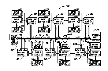
Fig. 1 shows a control system 30 using a plurality of data
link modules 32 constructed in accordance with the present
invention. The control system 30 is a hardware protocol
system, programmable through firmware, that is capable of
concurrently conveying single and multi-bit words of data. The
control system 30 has its communication capability distributed
among a plurality of the data link modules 32. As a result,
the use of a computer 34 to operate the control system 30
itself is optional. The control system 30 also includes a
master clock module 36 and a power supply 38 which are both
connected to a cable 40 preferably having four conductors. The
conductors include a direct current voltage power line 42, a
master clock line 44, a data bus 46 and a common 48 or the
power supply 38. The control system cable 40 is configured in
any shape required such as the configurations known as ring,
multidrop, loop back, bus and star. Of course, using ring or
loop back configurations provides a degree of redundancy. One
or more controlling or input devices 50, such as a photosensor
controlled switch, are connected to at least one of the data
link modules 32. A data link module 32 having an input device
50 connected to it acts as an input module for placing signals
on the data bus 46 on a serial multiplex time division basis in
response to local input signals from the input device. One or
more controlled, or output devices 54, such as a solenoid
controlled switch or the like, are connected to at least one of
the modules 32. A data link module 32 having an output device
54 connected to its local output acts as an output module for
extracting data from the data bus 46 on the serial multiplex
time division basis and for producing local output signals to
which the output device responds. Each data link module 32 has
up to two channels for either inputting signals to the data bus
W096/08801 ~ 5 PCT~S9S/12lS9
18
46 or outputting signals from the bus during a mode one time
slot 65 or a mode two time slot 67 shown in Figs. 17A-17E.
Fig. 1 shows, for simplicity of illustration, each data link
module 32 acting as either an input module or an output module,
as shown in Fig. 1. Alternatively, a data link module 32 can
act as both an input and an output module concurrently. In
such a case, an input device 50 connected to the data link
module 32 is associated with one of the channels and an output
device 54 connected to the data link module 32 is associated
with the other of the channels.
The data link module operates in either a mode one or a
mode two mode of operation. A timing diagram for mode one
operation is shown in Figs. 17A and 17B. The control system
30, Figs. 1, uses a clock signal timing protocol composed of an
elongated sync period 58 followed by up to 256 identical clock
cycles 61 labelled 0-256. The sync period 58 and the 256 clock
cycles 61 represent a frame 62. The master clock signal 85 is
generated by the master clock module 36 and is received by each
data link module 32 via the clock line 44 of bus 40. Each of
the up to 256 clock cycles 61 represents a potential device
address. Each data link module 32 selectively connects one or
more of the input devices 50 and one or more of the output
devices 54 to the data bus 46 during the time slot, or address,
65 associated with each such device 50 and 54. Depending upon
the mode of operation being mode one or mode two, the duration
of the address 65 is one or two cycles, respectively, of the
control system master clock signal 85. The number of clock
cycles 61 per frame 62 is selectable at the master clock module
36 and the number selected is equal to the number of different
addresses required. The fewest number of clock cycles 61
needed per frame 62 are selected to optimize the response time
of the control system 30.
~ WO96/08801 -- 2 ~ 7 6 1 3 5 PCT~S95,l2l59
' 19
Referring to Figs. 2A and 2B, each data link module 32
includes an integrated circuit 80. As shown in Figs. 17A and
17B, each mode one time slot or address 65 is one full master
clock cycle 61 in duration. In mode one, during the first part
of the time slot 65, data is placed on the data bus 46 by one
or more input data link modules 32 and the data remains on the
data bus 46 for the entire time slot. At the midpoint 64 of
the time slot 65, the data on the data bus 46 is copied from
the bus to output terminals 98 and 100 on at least one output
data link module 32 for use by at least one output device 54.
New data is placed on the data bus 46 at the end of the time
slot 65, i.e. at the beginning of the next time slot, and the
process continues for each time slot 65 of a frame 62. Without
multiplexing of frames 62, the process repeats itself during
subsequent frames. The operation of the process with
multiplexing of frames is described hereinafter.
The operation of the control system 30 using single bit
input and output signals is described fully in the aforesaid
patent of Riley which is hereby incorporated by reference.
However, unlike known data link modules designed for the
passing of single bits of data, the data link module 32 of the
present invention selectively passes either single bit or multi
bits of data. For example, a control system 30 using the data
link modules 32 is thereby enabled to ~ransfer a sixteen bit
word of data from an input device 50 to the data bus 46 and
from the data bus 46 to an output device 54 without using
complicated circuitry external to the integrated circuit 80 of
- the data link module 32. Unlike known data link modules, the
data link module 32 is programmable to permit any size word of
data up to 256 bits without any hardware change to the data
link module 32. In Fig. 1, the input and output devices are
WO96/08801 ~ 2 ~ 7 6 ~ 3 ~ PCT~S95/121S9 ~
represented as eight bit devices merely for simplicity of
illustration.
This multibit word feature allows the data link module 32
to easily interact with computer based input and output
devices, but without requiring a host computer 34 to operate
the control system 32 itself. The variable length words allow
the data link module 32 to interconnect popular 8, 16 and 32
bit devices by making firmwire changes but without making major
hardware changes. Analog data can be conveyed via the data bus
46 of the control system 30 by using multibit words and by
using an analog to digital converter (not shown) at an input
data link module 32 and a digital to analog converter (not
shown) at an output data link module 32.
In addition, a control system using the data link module
32 overcomes a limitation of known devices since it is capable
of controlling more than 256 input devices and more than 256
output devices by multiplexing frames 62 without complicated
circuitry external to the integrated circuit 80 of the data
link module 32.
The control system 30 using data link modules 32
constructed in accordance with the invention selectively
operates in mode one or mode two. In mode two, the four
conductors 42, 44, 46 and 48 of the control system cable 40 are
connected to an option host computer 34, preferably a
microprocessor based personal computer, via a single half-slot
industry standard architecture (ISA) computer interface card
(not shown). The control system 30 appears to the host
computer 34 as a 2048 byte block of dual-port random access
memory (RAM). The input and output is bit-mapped to an unused
location of RAM.
Referring now to the mode two composite timing diagram,
Figs. 17C and 17D, each mode two address 67 is twice as long
WO 96/08801 - PCT/US95/12159
~ ~176~35
21
(i.e. has twice the duration) as each mode one address 65, Fig.
17A. It should be noted that the scale of Figs. 17A and 17B is
not the same as the scale of Figs. 17C and 17D. Although the
mode two master clock cycles 61 appear shorter in Figs. 17C and
17D than they do in Figs. 17A and 17B, this is only for
convenience of illustration; the mode two master clock cycles
are the same duration as the mode one master clock cycles 61.
In mode two, an address 67, such as address "36" in Fig. 17E,
is defined by two master clock cycles 61 and 61', Fig. 17E. At
the beginning of the first 61 of the two successive clock
cycles 61 and 61' in the address 67, data is placed on the data
bus 46 by data link modules 32 acting as input modules. The
data is latched on the data bus 46 for the duration of the
first 61 of the two clock cycles 61 and 61'. The data is
copied from the data bus 46 by the optional host computer 34
during the first clock cycle 61. At the beginning of the
second clock cycle 61' of the address 67, the optional host
computer 34 places a signal on the data bus 46, and the signal
is latched for the duration of the second clock cycle 61'.
During the second clock cycle 61', data is copied from the data
bus 46 by a data link module 32 acting as an output module, and
the data is fed to the output device 54 connected to the data
link (output) module 32.
Unlike known data link modules, the data link module 32
can operate with a power supply 38 of either approximately
twelve volts or approximately 24 volts without requiring
adapters. And unlike known data link modules, the data link
module 32 can be directly connected to either input devices 50
that represent binary logic levels with 0-5 volts or 0-9 volts.
As shown in block form in Figs. 2A and 2B, the integrated
circuit 80 includes input terminals 84, 86, 88, 90, 92, 94 and
96 for receipt of a master clock signal, or CLOCK; data bus
WO96/08801 2 1 7 6 1 3 5 PCT~S9S/12159
: I
22
signals, or DATA; an operating voltage, or Vcc; a voltage
common, or COMMON, preferably at ground potentiali an external
oscillator resistor, (not shown); a channel A input signal, or
CH_A; and a channel B input signal, or CH_B, respectively. The
integrated circuit 80 has output terminals 98, 100, 102, 104,
106, 108, 110, and 112 for a channel A output signal, or
OUTPUT_A; a channel B output signal, or OUTPUT_B; a channel C
output signal, or OUTPUT_C; a shift clock in signal, or
SH_CLK_IN; a shift clock out signal, or SH_CLK_OUT; a multiplex
clock signal, or MUX; a mode/synchronizing signal, or
MODE_SYNC; and a data drive signal, or DATA_DRV, respectively.
Each data link module 32 has two channels, channel A and
channel B, and each channel is associated with an address.
During each time frame 62, an eight bit counter 114 shown in
Fig. 2A counts the cycles 61 of the master clock signal 85.
The eight bit counter 114 is reset at the beginning of each
frame 62. In mode one, each clock cycle 61 corresponds to an
address 65. In mode one, the counter 114 counts every clock
cycle 61 and the results are fed to address comparators 116 and
118 that compare the count of the counter with the respective
addresses for which the data link module 32 has been
programmed. When the count matches the address, the associated
comparator generates a coincidence A (COIN_A) and a coincidence
B (COIN_B) signal, respectively. In mode two, the operation is
similar except an address 67 consists of two clock cycles 61
and 61'. As shown in Fig. 2A, the window control section 120
of the integrated circuit 80 feeds a signal to the eight bit
counter 114 to compensate for the difference between mode one
and mode two.
The operation of the integrated circuit 80 will become
clear after the operation of the various sections of it,
represented by the blocks in Figs. 2A and 2B, are individually
~ WO96108801 - PCT~S951121Sg
2 ~ 7~ ~ 3~
described in detail hereinafter. Except when essential to
understanding the operation of the various circuits, the power
supply line 42 and the common line 48, are not shown in the
detailed diagrams of the circuits.
SIGNAL CONDITIONING
As shown in block form in Fig. 2A, the channel A input
signal at the channel A input terminal 94 to the integrated
circuit 80 is fed through a dual signal conditioning circuit
180 before further processing. The signal conditioning circuit
180 includes a Channel A signal conditioning circuit 122 (shown
in Fig. 3A) and a Channel B signal conditioning circuit (not
shown). As shown in Fig. 3A, the signal conditioning circuit
122 has an anti-aliasing filter 124, a hysteresis circuit 126,
and a digital low pass filter 128. The signal conditioning
circuit (not shown) for channel B is essentially identical to
the signal conditioning circuit 122 for channel A; therefore,
only the signal conditioning circuit for channel A will be
described in detail. The input terminal 130 of the signal
conditioning circuit is the input terminal 131 to the anti-
aliasing filter. The anti-aliasing filter 124 includes a
series resistor 136, preferably approximately 470 kQ, and a
capacitor 156 between the input 131 and ground potential,
preferably approximately 17 pF. Preferably, the invention of
the data link module 32 is used with channel A and channel B
input frequencies below 3 kHzi therefore, the anti-aliasing
filter 124 has a bandstop of approximately 30 kHz. The output
132 of the anti-aliasing filter 124 is fed into an input 134 of
the hysteresis circuit 126.
The hysteresis circuit 126 is programmable to accept a
signal having different voltage levels ranges at its input
terminal 134. A cell 138 of an electrically erasable read only
memory (EEPROM), not shown in its entirety in Fig. 3A, is
WO96/08801 2 1 76 1 35 PCT~S95tl215g ~
24
connected to another input 140 of the hysteresis circuit 126.
A logical zero at the cell 138 causes the acceptable input
voltage range to be 0-5 volts. A logical one at the cell 138
causes the acceptable input voltage range to be 0-9 volts. The
hysteresis`-circuit 126 prevents false state transitions due to
minor voltage level variations. The programmable hysteresis
circuit 126 and the cell 138 of the EEPROM function together as
a local input voltage range selector.
The hysteresis circuit 126, shown in more detail in
Fig. 3B, includes an inverter 142 for inverting the value
stored in the E~ cell 138, and a circuit 144 of eight resistors
and four transistors for producing two relatively high and two
relatively low voltages. The hysteresis circuit 126 is
preferably a 50% hysteresis circuit. The two relatively high
voltages, 6.75v and 3.75v, are 75% of the m~X;mum input voltage
expected in 9v systems and 5v systems, respectively. The two
relatively low voltages, 1.25v and 2.25v, are 25% of the
maximum input voltage expected in 9v systems and 5v systems,
respectively. Activation and deactivation of the EE cell 138
causes selection of one of the pair 6.75v and 2.25v and the
pair 3.75v and 1.25v for use by controlling comparators 146 and
148. One of the comparators 148 produces a comparator output
signal (HITRIP) 149 in response to a signal at the input
terminal 134 of the comparator 148 exceeding 75% of the maximum
input voltage. The input terminal 133 of the comparators 146
and 148 is connected to the input terminal 134 of the
hysteresis circuit 126. The comparator output signal tHITRIP)
149 sets a flip-flop 150. The Q output terminal 152 of the
flip-flop 150 is the output 136 terminal of the hysteresis
circuit 126. The output signal 135 of the hysteresis circuit
126 is a flat wave that remains high until the voltage of the
signal 125 at the input terminal 134 of the hysteresis circuit
~ WO96/08801 - PCT~S951121S9
217613~
falls below 25% of the maximum input voltage, at which time the
other comparator 146 produces another comparator output signal
(LOTRIP) 147 to reset the flip-flop 150 thereby bringing the
signal 135 at the output terminal 136 of the hysteresis circuit
to zero vd~lts. The signal 135 at the output terminal 136 of
the hysteresis circuit 126 is feed into an input terminal 154
of the digital filter 128. An output signal 159 from of an
internal oscillator 158 shown in block form in Fig. 2B is feed
into the digital filter 128 to control the bandstop of the
digital filter. The bandstop frequency is determined by the
frequency of the internal oscillator 158 divided by five.
Preferably, the frequency of the internal oscillator 158 is
approximately 150 kHz. The digital filter 128 is comprised of
a multi-bit, preferably five bit, serial-in, parallel-out shift
register 160. The output signal 163 from the shift register
160 is simultaneously presented to a positive pulse
consecutivity checker 162 and to a negative pulse consecutivity
checker 164, each comprised of a multi-input, preferably five-
input, AND gate 166 and 168, respectively. The positive pulse
consecutivity checker 162 produces a signal at input terminal S
170 of an RS flip-flop 172 only when a signal is extant during
each of a plurality of consecutive cycles of the internal
oscillator 158. The RS flip-flop 172 retains at output Q
terminal 174 a logical one output until reset by the negative
pulse consecutivity checker 164. The output Q terminal 174 of
the RS flip-flop 172 is connected to the output terminal 176 of
the channel A signal conditioning circuit 122. An IINPUT_A
signal, being a conditioned INPUT_A signal, is produced on the
output terminal 176 of the channel A signal conditioning
circuit 122. The output terminal 176 of the signal
conditioning circuit 122 for channel A and the output terminal
178 of the signal conditioning circuit (not shown) for channel
WO96/08801 ~ 7 6 t ~ 5 PCT~S95/12159
.
26
B are coupled to the channel A and the channel B, respectively,
input data control circuits 182 and 184.
The data bus 46 and master clock bus 44 conditioning
circuits 186 and 188, respectively, operate in a manner similar
to the channel A and B inputs signal conditioning circuit 122
(not shown) except for the frequencies involved. Preferably
the invention of the data link module 32 is used at clock bus
44 and data bus 46 frequencies below 200 kHz; therefore, the
data bus and clock bus anti-aliasing filters 186 and 188 have
an anti-aliasing filter resistor 126 o~ preferably 100 kQ and
the signal conditioning circuits preferably have a break point
of approximately 225 kHz. In a similar manner, the data bus
signal conditioning circuit 186 and the master clock bus signal
conditioning circuit 188 produce conditioned signals IDATA 191
and ICLOCK 192 from signals DATA 87 and CLOCK 85, respectively.
POWER ON RESET DELAY
Referring now to Fig. 2B, the internal oscillator 158 of
the integrated circuit 80 has a frequency range of preferably
50-400 kHz. The frequency is controlled by the external
resistor R (not shown) connected from input terminal 92 to
ground, where R (in ohms) - 14.5 x 10⁹/freq. (in Hertz).
Preferably, R is between 25 - 200 kQ. The internal oscillator
158 is of a type generally known and is not part of the
invention. The internal oscillator 158 produces a signal OSC
159.
As shown in block form in Fig. 2B, a power on reset delay
circuit 190 has three input terminals 181, 183 and 185 for
receipt of the oscillator signal (OSC) 159, the internal master
clock signal (ICLOCK) 192, and a power on reset signal (POR)
- 30 194. The POR signal 194 occurs immediately after application
- of power to the integrated circuit 80 and is produced by one of
several well known power-on-reset means 195 and is not part of
WO96/08801 PCT~S95/12159
~ 2176135
the invention. The power on reset delay circuit 190 has two
output terminals 216 and 218 for outputting a synchronous
signal (SYNC) 196 and a power on reset delay signal (POR_DLY)
198, respectively.
The power on reset delay circuit 190 is shown in detail in
Fig. 4. The internal master clock signal (ICLOCK) 192 is held
high for a preselected sync period 58 in order to define the
beginning of each time frame 62. Preferably, the sync period
58 has a duration of eight master clock cycles 61. A four bit
counter 200 and a NAND gate 202 produce a-low SYNC_DET signal
205 at the output terminal 204 of the NAND gate 202 upon
receiving ten cycles of the OSC signal 159 while ICLOCK 192 is,
during the same interval, continuously high. The ICLOCK signal
192 is fed into an inverted clear input 183 of the counter 200.
The SYNC_DET signal 205 remains low for a period dependent upon
the relationship between the ICLOCK frequency and the OSC
frequency; however, on the first negative transition of ICLOCK,
which defines the end of the sync period 58, SYNC_DET become
high again because the negative ICLOCK pulse clears the counter
200. Preferably, the OSC frequency is one and one-half to ten
times faster than the ICLOCK frequency.
The SYN_DET signal 205 is fed into a plurality of
interconnected data flip-flops 206 and 208 and then into an AND
gate 210. The flip-flops 206 and 208 are cleared upon receipt
of the low POR signal 194 at flip-flop inputs 209 and 211,
respectively. The output 212 of the AND gate 210 produces the
low POR_DLY signal 198 immediately after receipt of the low POR
signal 194. The output 212 of the AND gate 210 produces a high
POR_DLY signal 198 after the plurality of data flip-flops 206
and 208 receive a plurality of SYNC_DET signals via gate 201.
The circuit shown in Fig. 4 produces the high POR_DLY
signal 198 after receiving three SYNC_D~T signals 205.
WO96/08801 2 ~ 76 ~ 35 PcT~s95ll2ls9
.. . . .
28
Although only two data flip-flops 206 and 208 are shown in
Fig. 4 for simplicity, it is preferable to have approximately
12 data ~lip-flops for counting 4,095 SYNC_DET signals 205
prior to producing the high POR_DLY signal 198. The power on
reset delay circuit 190 produces the POR_DLY signal 198 after
the integrated circuit 80 receives a preselected plurality of
SYNC_DET signals 205 after application of power to the
integrated circuit. The POR_DLY signal 198 and the SYNC_DET
205 signal are gated through an AND gate 21~ to produce a SYNC
signal 196 at the output 216. Therefore, SYNC 196 remains low
unless POR_DLY 198 is high.
Many of the flip-flops of the integrated circuit 80 are
either preset or cleared by SYNC 196; therefore, these flip-
flops are advantageously preset or cleared only after the power
1~ supply to the data link module 32 has stabilized. The POR_DLY
signal 198 is fed to the clock loss output lock circuit 240, to
the safety input inhibit protection circuit 220, and to the
mode/sync circuit 458.
SAFETY INPUT PROTECTION CIRCUIT
As shown in block form in Figs. 2A and 2B, the safety
input protection circuit or input inhibit circuit 220 prevents
the input data control circuits 182 and 184 from responding to
input signals during a preselected period of time after power
is applied to the integrated circuit 80 and also during the
_ 25 period of time that the integrated circuit is being programmed
or the programming is being verified. As shown in more detail
in Fig. 5, the input inhibit circuit 220 has an NOR gate 224
having the active low POR_DLY signal 198 and an active high
program/verify mode signal (P/V_MODE) 199 as inputs fed into
30 input terminals 226 and 228, respectively, and having an
INPUT_INHIBIT signal 229 as an output signal at output terminal
_ 230.
~ WO96/08801 PCT~S95112159
217~!35
29
The low POR_DLY signal 198 is produced by the power on
reset delay circuit 190 for a preselected period of time after
power is applied to the integrated circuit 80. A high P/V_MODE
signal 199 is produced by the module programmer 232 during the
programming cycle and during the verifying cycle. The POR_DLY
signal 198 and the P/V_MODE signal 199 are applied to the
inputs 226 and 228 of the input inhibit circuit 220. The
output terminal 230 of the input inhibit circuit 220 is coupled
to input terminals 416 and 418 of the channel A and channel B
input data control circuits, 182 and 184, respectively. The
input inhibit circuit 220 works in conjunction with the channel
A and channel B input data control circuits, 182 and 184,
respectively. The operation of the channel A input data
control circuit is essentially the same as the operation of the
channel B input data control circuit so only the channel A
circuit will be described in detail. As shown in Fig. 5, the
INPUT_INHIBIT signal 229 at the input terminal 416 is fed into
an inverted clear (CLR) terminal 235 of a flip-flop 400. As a
result, a signal at an output Q terminal 406 of the flip-flop
400 becomes zero when either the signal POR_DLY 198 is low or
the signal P/V_MODE 199 is high. Therefore, the subsequent
stages of the integrated circuit 80 will not respond to input A
or input B signals under preselected conditions to enhance
safety and reliability of the data link module 32. Preferably,
the preselected conditions are when either the signal POR_DLY
198 is low or when the signal P/V_MODE 199 is high.
CLOCK LOSS OUTPUT LOCK
It is advantageous to prevent signals at the output
terminals 98, 100, 102, 104, 106 and 108 of the integrated
circuit 80 from changing in the absence of the master clock
signal 85. The integrated circuit 80 has a clock loss detect
circuit 240 sho~n in block form in Fig. 2B. The clock loss
WO96/08801 : ` 2 ~ 76 ~ 35 PCT~S95/12159 ~
detect circuit 240 shown in more detail in Fig. 6 has three
input terminals 221-223 for receipt of ICLOCK 192, OSC 159 and
POR_DLY 198 signals and one output terminal 225 producing a
long reset signal (LONG_RST) 241. The clock loss detect
circuit 240 includes a thirteen bit counter 242 which starts to
count the cycles of OSC 159 i~ there is a loss of the internal
master clock signal ICLOCK 192. The OSC signal 159 is fed to
the clocking pin 244 of the thirteen bit counter 242. The loss
of ICLOCK 192 is determined by a delay element (DLY) 245 and an
exclusive-OR gate 246 connected to the clear (CLR) pin 248 of
the counter 242. When ICLOCK 192 is extant, the counter 242 is
cleared on every transition of ICLOCK. Upon counting 6,144
cycles of the OSC signal 159, outputs 250 and 252 of the
counter 242, representing the twelfth and thirteen bits of the
number 6,144 in binary, are high which causes a NAND gate 256
to produce a low clock loss delay (CLK_LOSS_DLY) signal at its
output 254~
The clock loss detect circuit 240 begins to produce a low
CLK_LOSS_DLY signal commencing 6,144 cycles of OSC after loss
of the master clock signal and the circuit continues to produce
the low CLK_LOSS DLY signal until reinstatement of the master
clock signal. The POR_DLY signal and the CLK_LOSS_DLY signal
are coupled through an AND gate 258 to produce a long reset
(LONG_RST) signal. The LONG_RST signal is fed to the repeat
_ 25 circuit 260 and to the safety output protection circuit 262.
SAFETY OUTPUT PROTECTION CIRCUIT
It is important to prevent the multiplex clock 108, shift
- clock out 106, shift clock in 104, the A, B, and the C outputs
98, 100 and 102 terminals from outputting under certain
-30 conditions. As shown in block form in Fig. 2B, the integrated
-circuit 80 has a safety output protection circuit 262 that
prevents the output terminals 98, 100, 102, 104, 106 and 108 of
~ WO96/~8801 - = 2 1 76 1 35 PCT~S9S/121S9
31
the integrated circuit 80 from having an output signal in the
presence of either a low LONG_RST signal or during programming
or verifying of the programming.
As shown in more detail in Fig. 7, the safety output
protection circuit 262 has three input terminals 264, 266 and
268 for receiving SYNC, LONG_RST and a program voltage enable
(PVE) signal, respectively. The control system power line
voltage Vcc is applied continuously to a D input terminal 270
of a data flip-flop 272. The data flip-flop 272 produces a
high output inhibit signal at Q 274 as a result of the voltage
Vcc applied to the D input terminal 270 of the flip-flop 272,
except when cleared by one of a high PVE signal and a low
LONG_RST signal. The circuit also includes an NOR gate 276
that combines the high PVE and the low LONG_RST signals to form
one reset signal at the NOR gate output terminal 277 prior to
the signals being applied to a clear pin 278 of flip-flop 272.
A low reset signal clears the flip-flop 272. The SYNC signal
enables the flip-flop 272 at the beginning of each frame 62 and
as a result the flip-flop is set by the first SYNC signal after
the reset signal is removed. Referring now to Figs. 2A and 2B,
the output of the safety output protection circuit 272 is an
output inhibit signal (OUTPUT INHIBIT) 280 which is fed to a
tristate device at each of the output terminals 98, 100, 102,
104, 106 and 108, respectively, forcing those output terminals
of the integrated circuit 80 into a high impedance state. The
high impedance state of the output terminals 98, 100, 102, 104,
106, and 108 is indicative of an absence of both a high signal
and a low signal at the output terminals.
DATA VERIFIER
Referring to Fig. 8, the repeat circuit, or data verifier,
260 shown in block form in Fig. 2A has a channel A data
verifier 288 and a channel B data verifier 289 which is
.
WO96/08801 ` PCT~S9S/12159
substantially identical to the channel A data verifier. In
order to avoid erroneous responses to random noise which may be
present on the data bus 46 during a selected time slot 65 and
67 associated with one of the modules 32, the data verifier 260
selectively requires a repetition of the same data signal 87 on
the data bus 46 during the time slot 65 and 67 associated with
the data link module 32 for a selected plurality of
successively contiguous time frames 62, 62' and 62", Fig 21.
Only after said repetition will the appropriate channel A or
channel B output signal change in response to the data signals
87 on the data bus 46. Still referring to Fig. 8, the channel
A data verifier 288 includes a plurality of binary data flip-
flops 282, 284 and 286 interconnected to form a multistage
shift register. Each of the data flip-flops 282, 284 and 286
stores the signal 87 present on the data bus 46 during each one
of a plurality of successive time frames 62, 62' and 62",
Fig. 21. The input terminals 290, 292, 294, and 298, Fig. 8,
of the channel A data verifier receive the signals from the
data bus 46, from a pair of electrically erasable read only
memories, or EE cells, 320 and 322 of an EEPROM 354, and from
the clock loss circuit 240, respectively.
Input terminal 296 of the channel A data verifier receives an
enabling clock pulse 302 produced on the output 303 of an AND
gate 304. The AND gate 304 has three inputs 311, 313, and 315
for receiving ICLOCK, COIN_A and OUTPUT_WINDOW signals,
respectively. The selected mode of operation, mode 1 or
mode 2, determines the nature and timing of these signals.
In mode 1, there is one clock cycle 61 per time slot 65.
The OUTPUT_WINDOW signal is continuously low, and an inverter
312 at input 311 permits the 3-input AND gate 30~ to be
= continuously enabled. Another inverter 314 at input 315
inverts the ICLOCK signal 192 to ena~le the three-input AND
~ WO96/08801 . ' 2176135 PCT~S95/121S9
33
gate 310 during only the second half of the clock cycle 61 when
ICLOCK is low. The COIN_A signal is high only during the
occurrence of the selected time slot 65 associated with the
data link module 32. The edge sensitive data flip-flops 282,
284 and 286 are enabled when COIN_A transitions from low to
high. The data flip-flops 282, 284 and 286 are enabled during,
and only during, the selected time slot 65 associated with the
data link module 32.
In mode 2, there are two clock cycles 67 and 67' per time
slot 67. In mode 2, during the first clock cycle 61, the
OUTPUT_WINDOW signal is high and during the second clock 61'
cycle the OUTPUT_WINDOW signal is low. Therefore, the three-
input AND gate 304 is activated only during the second 61' of
the two clock cycles 67 and 67'. In other respects, the data
verifier 260 works the same in mode two as it does in mode one.
The enabling clock pulse 302 enables each of the three
data flip-flops 282, 284 and 286 during the time slot, one of
65 and 67, associated with channel A of the data link module
32, but within successive frames 62, 62' and 62", Fig. 21.
Initially, the data flip-flops 282, 286 and 288 are preset by a
LONG_RESET signal from the circuit of Fig. 6. Thereafter, upon
the first occurrence of the time slot 61 of channel A of the
data link module 32, the data signal on the data bus will
appear at the Q output 324 of the first flip-flop 282 and also
at the D input 316 of a repeat circuit output flip-flop 318.
The signal 87 on the data bus 46 during the most recent frame,
one of 62, 62' and 62", will always be reproduced at the D
input 316 of the repeat circuit output flip-flop 318, but the
repeat circuit output flip-flop 318 will be enabled only upon
the occurrence of the enabling clock pulse 302 from output 303
of AND gate 304. The occurrence of the enabling clock pulse
WO96/08801 - 2 ~ 7 ~ ~ 35 PCT~S95/12159 ~
34
302 at the repeat c1rcuit output flip-flop 318 is controlled by
programming.
When the EE cell 320 is programmed to contain a logical
zero, an AND gate 338 switches its output 336 to a logical
zero, and~an output 340 of NAND gate 342 switched high during
the second half of each clock cycle 61 to enable the repeat
circuit output flip-flop 318, without any repetition of data,
at a time one-half of a clock cycle 61 after the activation of
the first flip-flop 282. When the EE cell 320 is programmed to
contain a logical one and an EE cell 322 is programmed to
contain a logical zero, the clock of the output flip-flop 318
will be enabled only if both the first and second flip-flops
282 and 284 have the same Q outputs. The first 282 and second
284 flip-flops will have the same Q output only if the data
signal 87 on the data bus 46 has been repeated in the selected
time slot, one of 65 and 67, in each of two successive frames
62 and 62'. The Q outputs 324 and 326 of the first and second
flip-flops 282 and 284, respectively, are fed into an
exclusive-OR gate 328.
The signal produced on the output 330 of the exclusive OR
gate 328, in combination with the signal produced on the output
of a NOR gate 344 and a NAND gate 346 and the state of the EE
cells 320 and 322 will cause the repeat circuit output flip-
flop 318 to be enabled immediately after (i.e. one-half clock
cycle 61 after) a frame 62' having a second consecutive
repetition of data signals 87.
When both EE cells 320 and 322 are programmed to contain a
logical one, the clocking pin of the repeat circuit output
flip-flop 318 is enabled immediately after (one-half clock
cycle 61 after) a third ~rame 62", only if the first, second
and third flip-flops have the same signals on their Q outputs
324, 326 and 332, respectively. The signal on output 232 of
~ WO96/08801 2 ~ 7 6 1 3 5 PCT~S951121S9
flip-flop 286 is fed into an exclusive-OR gate 348 along with
the signal on output 324 of flip-flop 282. The signal on
output 349 of gate 348 is low only when there is an identity of
data between the first 62 and third frames 62".
Table l summarizes the effect on the data verifier of
programming EE cells 320 and 322.
TABLE l
EE CELL 320 322
No Repetitions 0 0 or l
One Repetition l o
Two Repetitions
In a similar manner, if needed, the data verifier 260 is
extended to recognize and selectively respond to more than a
minimum of three occurrences of the same data signals 87 on
consecutive frames 62 by adding more flip-flops and more EE
cells and their associated programmable logic circuitry.
POLARITY SELECTOR CIRCUIT
In order to overcome the deficiencies of the C output
terminal of known data link modules, the data link module 32
has a combinational logic circuit polarity selector 350, shown
in block form in Fig. 2B, comprising a polarity independent
circuit 352, Fig. 9. The polarity independent circuit 352
receives the A_OUTPUT signal and the B_OUTPUT signal from the
data verifier 260 and also receives polarity selection
information from the EEPROM 354. As shown in detail in Fig. 9,
the polarity independent circuit 352 includes an AND gate 356
having two input terminals 358 and 360 for receiving the
A_OUTPUT and B_OUTPUT signals and having an output terminal 362
for producing a C_OUTPUT signal. Unlike known data link
WO96/08801 A , _ ~ ~ 7 6 t 3 5 P CT~ s95ll2lss
36
modules, the polarities of the input signals to the AND gate
356 of the invention are not restricted to being the same as
the polarities of the A_OUTPUT and B_OUTPUT signals. The
polarity of each input to the AND gate 356 can be individually,
selectively changed from the polarities of the A_OUTPUT and
B_OUTPUT signals. Polarity selection information from one of
the EE cells 364 and the A OUTPUT signal are fed into an
exclusive-OR gate 366. The output 368 of the exclusive-OR gate
produces the A_OUTPUT signal but with a polarity selectively
different than its input polarity. Similarly, the B-OUTPUT
signal and a second EE cell 370 is fed through another
exclusive-OR gate 372. The polarity of the output of the AND
gate 356 is selectively controlled by a third EE cell 374 and
an exclusive-OR gate 375 thereby allowing C_OUTPUT signal to be
any logical combinational function of the A_OUTPUT signal and
B OUTPUT signal.
INPUT SYNCHRONIZER
Referring now to Fig. 2A, the integrated circuit 80 has
input data control circuits 182 and 184 to isolate subsequent
portions of the integrated circuit from changes in channel A
and channel B input signals occurring during a time slot 65
associated with a data link module 32. The channel A input
data control circuit 182 is substantially identical to the
channel B input data control circuit 184, therefore only the
channel A input data control circuit will be described in
detail. The channel A input data control circuit 182 has
COIN_A, IINPUT_A, INPUT_WINDOW, and INPUT_INHIBIT signals as
inputs and a INPUT_DATA_A signal as an output. As shown in
more detail in Fig. 5, the input data control circuit 182 has a
data flip-flop 400 and a three-input AND gate 402. The
= IINPUT_A signal is ~ed into the D input 404 of the data flip-
flop 400 which is enabled by the COIN_A signal only at the
WO96/08801 -i PCT~S95/121S9
2l76~35
37
beginning of the time slot 65 associated with the data link
module 32. The COIN_A signal is normally low and goes high
only during the address associated with the data link module
32. The data flip-flop 400 is edge sensitive. At the rising
edge of the COIN_A signal the state of the IINPUT_A signal is
latched onto a Q output 406 of the flip-flop 400 for the
duration of the time slot 65 of the data link module 32. The Q
output 406 is fed into the three-input AND gate 402 along with
COIN_A and INPUT_WINDOW. In mode one, INPUT_WINDOW is
continuously low and the inverter 408 at one of the inputs 410
of the AND gate 402 allows the AND gate to be enabled by
INPUT_WINDOW. During the time slot 65 of the data link module
32, COIN_A is high and the AND gate 402 is enabled by COIN_A
during the module's time slot. Therefore, in mode one, the
IINPUT_A signal appears at the output terminal 412 of the AND
gate 402 only during the time slot 65 of the data link module
32. Referring now to the timing diagram, Figs. 17C and 17D, in
mode two, each time slot 67 is twice as long as each timë slot
65 in mode one, but only the first half of each mode two time
slot 67 is dedicated to applying input signals to the data bus
46. In mode two, INPUT_WINDOW operates at half the frequency
of the master clock signal 85. In mode two, INPUT_WINDOW is
low during the first half of the time slot 67 and high during
the second half of the time slot. Referring again to Fig. 5,
the inverter 408 on the input 410 to the AND gate 402 allows
the AND gate to be enabled only during the first half of the
time slot 67 of the data link module 32. Therefore, in mode 2,
the IINPUT_A signal appears at the output 412 of the AND gate
402 only during the first half of the time slot 67 of the data
link module 32. The output 412 of the AND gate 402 forms the
output terminal 414 of the input data control circuit 182 at
WO 96tO8801 ~ 2 ~ 7 6 ~ ~ ~ PCT~S95/121S9
..
38
which is produced the signal INPUT_DATA_A. The INPUT_DATA_A
signal is fed to the data bus drive circuit 420.
MODE SELECTION INDICATOR
Referring now to Fig. 15, in order to synchronize the
operation of other components, such as shift registers 588 and
590, on the data link module 32 with the operation of the
integrated circuit 80 and in order to inform the other
components on the module of the mode of operation, the
integrated circuit has a single terminal 110 for alternately
conveying a SYNC signal 196 and a MODE signal 488. As shown in
block form in Fig. 2B, the combined MODE/SYNC signal 456 is
generated by a mode/sync output circuit 458. The mode/sync
output circuit 458 has four input terminals for receipt of MODE
488, SYNC 196, OSC 136, and POR_DLY 198 as input signals and
one output terminal 468 for producing the combined MODE/SYNC as
an output signal 456. Advantageously, the MODE/SYNC signal 456
is independent of the channel A and channel B input signals,
and of the data signals 87 on the data bus 46. The MODE/SYNC
output terminal 468 periodically produces a SYNC output signal
196 whenever the integrated circuit 80 has operating power,
except for a short period of time immediately after start up
due to a low POR_DLY signal. Of course, there can be no sync
information on the MODE/SYNC output terminal 468 if the
integrated circuit 80 loses the master clock signal 85, but the
mode information will remain on the MODE/SYNC output terminal
468 in such an event.
The mode/sync output circuit 458 is shown in more detail
in Fig. 10. The low POR_DLY clears a data flip-flop 476. An
inverted SYNC signal 196 and a delayed SYNC signal 196 are fed
into an AND gate 474 to produce a positive short duration pulse
on a transition when SYNC falls low. The short duration pulse
presets the data flip-flop 476. A D input 478 of the flip-flop
~ WO96/08801 PCT~S95/121ss
39 2176~35
476 is continuously at ground potential. The OSC signal 136 is
fed into the clocking input 480 of the flip-flop 476.
Therefore, the Q output 482 of the flip-flop 476 is normally
low but it is preset high by the short duration pulse at the
beginning of every frame. However, the output Q 482 of the
flip-flop 476 remains high for only one cycle of OSC 136 and
then it returns low. The Q output 482 of the flip-flop 476
goes into an exclusive-OR gate 484 along with the MODE signal
488. The MODE signal reflects the mode selected and stored in
the EEPROM 354 during programming. In mode one, MODE = 0 and
the exclusive-OR gate 484 effectively inverts the Q output 482
of the flip-flop 476. In mode two, MODE = 1 and the exclusive-
OR gate 484 does not change the Q output 482 of the flip-flop
476. An inverter/buffer 486 inverts theMODE /SYNC signal 456',
regardless of mode, prior to the MODE/SYNC signal 456 appearing
on the MODE/SYNC output terminal 110 of the integrated circuit
80. As shown on the timing diagram, Figs. 17A and 17B, in mode
one, MODE/SYNC 456 is continuously low, except that it goes
high for one cycle of OSC 136 at the beginning of each frame
62. In mode two, MODE/SYNC 456 is continuously high, except
that it goes low for one cycle of OSC 136 at the beginning of
each frame 62.
MULTIPLEXING FRAME IDENTIFIER
Referring now to Fig. 21, multiplexing of frames 62 allows
a successive frame 62' to convey different data than the data
conveyed by a preceding frame 62. Referring now to Fig. 2A,
the integrated circuit 80 has a multiplex clock circuit 490 for
generating a multiplex clock signal 492 needed to multiplex
frames 62. The integrated circuit 80 also provides an output
terminal 108 so that the multiplex clock signal (MUX_CLK) 492
could be accessed by relatively few and relatively simple
external components on the data link module 32. This feature
WO g6/08801 2 ~ 7 6 ~ 3 5 PCT~S95/12159
:
overcomes one of the disadvantages of the prior out, which
required similar signals to be generated by additional external
and delicate components.
Referring now to Fig. 16, integrated circuit 80 has a
multiplex address clock output terminal 108 for use by a
decoder 494 on the data link module 32 for selectively enabling
a plurality of shift registers 496, 498 and 500. Each of the
plurality of shift registers 496, 498 and 500 transfers data
from the data bus 46 to an associated output field device 54,
54', 54" during the same time slots 65 but within different
frames 62. The use of the MUX_CLK signal 492 permits time
division multiplexing of frames 62. When time division
multiplexing is done, each frame 62 is given a frame number.
Time slots 1-4, inclusive, are used to number each frame 62.
Time slot 0 is not used in frame multiplexing. The master
clock module 36, Fig. 1, places the frame number on each frame
62 by putting a series of four signals, representative of the
frame number, on the data bus during time slots 1-4 of each
frame. Because four bits are used to assign frame numbers, up
to sixteen different numbers can be assigned to frames. The
multiplexing of 16 frames allows for the serial transmission of
up to 3,840 bits of data tl6 x 240 bits per frame). Although
the present embodiment uses four time slots for multiplexing up
to 15 frames, it is possible to use up to sixteen time slots
for multiplexing up to 32,768 frames to convey up to 7,864,320
bits of data ~32,768 x 240 bits per frame).
As shown in block form in Fig. 2A, the multiplex clock
circuit 490 has eight parallel input terminals 501-508 for
acceptance of eight-bit frame addresses, and terminals 509, 510
and 511 for acceptance of SYNC, ICLOCK and OUTPUT_WINDOW
signals, respectively. The circuit has one output terminal 513
for outputting a multiplex clock (MUX_CLK) signal 492.
_ WO96/08801 ~ PCT~S95/12159
- 2176135
41
As shown in more detail in Fig. 11, the multiplex clock
circuit 490 includes an eight-input 501-508 NAND gate 514 with
six inputs having inverters for detecting a frame 62 having a
frame number 00000101 = 5. The NAND gate 514 produces a
COUNT_5 signal which is normally high but which is low for one
master clock cycle 61 after detecting the frame with the frame
number five.
The SYNC signal 196 sets an RS flip-flop 512 at the
beginning of each frame 62 which produces a high output at Q
515 which, in turn, enables a three-input AND gate 516. In
mode one, the OUTPUT_WINDOW signal 121 is continuously low and
also enables the three-input AND gate 516. The combination of
the SYNC 196 and OUTPUT_WINDOW 121 signals enables ICLOCK 192
to be reproduced at the output terminal 513 of the multiplex
clock circuit 490 until the fifth frame is counted by counter
114. When the fifth frame is counted a COUNT_5 signal is
produced by NAND gate 514, and flip-flop 512 is reset. The
output Q of flip-flop 512 becomes zero thereby disenabling the
three-input AND gate 516 after counter 114 counts five frames
62. After the fifth frame 62, no MUX_CLK signal 492 is
produced.
In mode two, the multiplex clock circuit 490 works similar
except that OUTPUT_WINDOW 121 is a clocking signal operating at
half the frequency of ICLOCK 192 and in phase with ICLOCK. In
mode two, the three-input AND gate 516 enables ICLOCK 192 to
pass through to the multiplex clock output terminal 513 only
when both OUTPUT_WINDOW and ICLOCK are both negative. As shown
on the timing diagram, Fig. 17C, in mode two, MUX_CLK 492' is a
train of positive and negative pulses of dissimilar width.
As shown in Fig. 16, the MUX_CLK signal 492 is fed into an
input 518 of the decoder 494. The data bus is connected to
another input 519 of the decoder 494. The MUX_CLK signal 492
WO96/08801 2 ~ 76 PCT~S95112159
42
allows the decoder 494 to serially receive the frame numbers
from the data bus 46 during time slots 1-4. The output of the
decoder 494 has up to 16 individual lines for successively
enabling one of each of the shift registers 496, 498 and 500
during the frame 62 associated with each shift register.
PROGRAMMING
The logic circuits of the integrated circuit 80 operate on
a preselected internal DC voltage, preferably approximate 9
volts. As shown in block form in Fig. 2B, the integrated
circuit 80 has a voltage regulator 520 that accepts an input DC
voltage Vcc from 12 to 32 volts and produces the internal DC
operating voltage V or Vref of approximately 9 volts. The
voltage regulator 520 is one of several known types and forms
no part of the invention. The signal passing circuitry of the
integrated circuit 80 is activated for passing signals through
the data link module 32 when Vcc is within one of two voltage
ranges. Preferably the two ranges are approximately 12-15
volts and approximately 18-32 volts. The DC input voltage Vcc
and the reference voltage Vref are fed into a module programmer
232 shown in block form in Fig. 2B. The other input signals
fed into the module programmer are POR, IDATA, ICLOCK,
LONG_RST, .2ICLOCK and input signals ~rom the EEPROM 354. The
output signals from the module programmer are a program voltage
enable signal (PVE), a program/verify mode signal (P/V_MODE), a
program/verify data signal (P/V_DATA) and output signals to the
= EEPROM 354.
The module programmer 232 is shown in more detail in
Fig. 12. The module programmer has a program enabler including
a voltage divider 530 having three resistors for producing two
voltages intermediate Vcc and ground. One of the two
intermediate voltages is fed into a positive input 531 of a
voltage comparator 532 having as its other input Vref. The
WO96/08801 2 1 7 6 ~ 35 PCT~Sg5/121S9
43
other of the two intermediate voltages is fed into a negative
input 533 of another voltage comparator 534 having as its other
input Vref. When Vcc is between approximately 15.5 - 17.5
volts, the outputs of each voltage comparator 532 and 534 is
high and ~ high PVE signal is produced at the output of an AND
gate 536. The module programmer also includes four flip-flops
538, 540, 542 and 544, a four bit counter 546, a five bit
counter 548, a serial-to-parallel converter 550, a parallel to
serial converter 552, a state machine 553 and at least eleven
logic gates 554-565 described in more detail hereinafter. The
four bit counter 546 is enabled by a low LONG_RST (which
indicates no clock signal transitions) and it counts 15
transitions of the data line while Vcc is between 15.5 and 17.5
volts. The four bit counter 546 is cleared by any transition
of the clock signal detected by a delay element 566 and an
exclusive - OR gate 555. The four bit output of the counter
546 is AND'd together by gate 556 to set a flip-flop 538. The
flip-flop 538 is normally in a reset state except when the
integrated circuit 80 is to be programmed or the programming is
to be verified in which case the flip-flop is set by the output
of the four-bit counter 546. The normally high LONG_RST is fed
into a delay element 570 and a gate 557 whose output is
momentarily low on any negative-going transition of LONG_RST
and the output is fed into a three-input AND gate 558. The
other inputs to the three-input AND gate 558 are PVE (a high
PVE is an indication that the integrated circuit 80 is ready
for programming) and an end of busy (EOB) signal. The LONG_RST
signal is required to be high prior to programming. However,
the momentary low on the LONG_RST input will cause the flip-
flop 538 to reset thereby preventing programming. When thethree inputs to the AND gate 558 are high, the reset signal to
the flip-flop 538 is removed and one of the preliminary steps
WO96/08801 ' ~1 7 6 ~ 3 5 PCT~S9S/12159
44
prior to programming is completed. Receipt of fifteen pulses
on the data line 46 is also required to cause the integrated
circuit 80 to become ready for programming. Upon receipt of
the fifteen pulses, the four bit counter 546 produces an output
to set the flip-flop 538. The Q output of the flip-flop 538 is
designated a PV_MODE signal. As shown on the timing dlagram,
Fig. 18A, the P/V_MODE signal from FFl 538 transitions from low
to high at this point 539. A high PV_MODE is indicative of
programming or verifying in progress. A low output Q of the
flip-flop 538 clears a second flip-flop 540.
The programming data is shifted into the data link module
integrated circuit 80 of the data link module 32 by using the
clock line 44 and data bus 46. As shown in the timing diagram
of Fig. 18A-18C, the data stream contains a program/verify
(P/V) bit and 32 data bits. The first bit is the P/V bit. The
P/V bit is low for programming; the P/V bit is high for
verifying. Flip-flop 540 is enabled by ICLOCK and is set when
the first programming bit is high. The first 16 bits contain
the addresses for channel A and B (eight bits each). The next
16 bits contain the control functions including output A to C
polarity, output B to C polarity, mode selection, channel A
repeat once, channel A repeat twice, channel B repeat once,
channel B repeat twice, and input A/B high select. The
positive true data is placed on the data line at the beginning
of the clock cycle (the positive going edge) and is transferred
to the integrated circuit at 180 (negative going edge) of the
clock cycle. If the P/V bit is high, the next 32 clock cycles
will shift the programmed data to the data line. A third flip-
flop 542 generates a COUNT OF_ONE signal which enables the
five-bit counter 548 to count to 32 which is the number of
programming bits. The third flip-flop 542 also enables a
serial-to-parallel converter 550 which receives serial data
~ WO96/08801 2 1 7 6 1 3 5 PCT~S95/121S9
from the data bus during programming, that is, when R/W is low
and SH_EN is low. Data from EE cells (not shown) of the EEPROM
354 is returned to a parallel-to-serial converter 552 for
extraction from the integrated circuit 80 via an AND gate 559
and an output OR gate 560 during verification of programming.
When the Q output of the second flip-flop 540 is low, an AND
gate 561 is enabled and the EE cells are written to. When the
Q output of the second flip-flop 540 is high, AND gate 559 is
enabled and the EE cells are read. The output of the AND gate
559 is fed into OR gate 560 for outputting data to the data
drive circuit 420 shown in Fig. 14. A five-bit counter 548
counts 32 clock cycles thereby enabling AND gate 565 which, in
turn, enables gate 561. When the AND gate 561 is enabled, it
provides timing to a fourth flip-flop 544 for use in a state
machine 553. The output of the fourth flip-flop 544 provides a
program ready signal (PROG_RDY) to the state machine 553. As
shown in the timing diagram, Fig. 18C, the PROG_RDY signal goes
high during the electrically erasable program cycle 574. The
state machine 553 controls the burning in of the EE cells
through a programming control logic circuit 572. The state
machine 553 has an output OBUSY that clears flip-flop 544
through gates 562 and 563 and delay element 568. Each data bit
will be placed on the data line 46 at the beginning of each
clock cycle where it can be read by a programmer. This data is
negative true.
The programming supply voltage at the integrated circuit
80 must be 16.5 Vdc + 1.0 Vdc. Preferably, a buffer resister
of 300 n (not shown) is used between the bus and the
integrated circuit 80. The voltage loss across this resistor
is approximately 0.4 Vdc. The supply voltage compensates for
this loss.
W096/0880~ 76 ~ 35 PCT~S95/121Ss
46
The voltage levels for the two control lines (clock line
44 and data line 46) swings between bus common and the internal
operating voltage V of the integrated circuit 80. This voltage
is pre~erably nine volts. A 100k Q resistor (not shown) is
part of each input ~ilter 188 and 186 for the clock lines 44
and data line 46, respectively. These resistors are also used
for input protection for the integrated circuit 80. This will
allow an input signal of several hundred volts without damaging
the integrated circuit 80 or causing improper operation. To
make the programmer clock and data signals compatible with the
prior art data link module described in the aforesaid patent of
Riley, a 12 volt signal is used. During programming, the clock
frequency is between 25 kHz and 30 kHz. The clock frequency is
used for timing reference in writing to the EEPROM 354.
As shown in the timing diagram for the program cycle,
Fig. 18C, after the data has been shifted into the integrated
circuit 80, the electrically erasable programming cycle 574
requires 2 cycles of 200 ms each. The first cycle is an erase
cycle, the second cycle is the programming of the EEPROM 354.
The output of the four-input AND gate 564 is fed into the
enabling clock input of the serial-to-parallel converter 550.
The programming time for each integrated circuit 80 is
approximately 500 ms.
The method of programming the data link module over the
data bus line 46 and the master clock line 44 includes: Step
one, removing the power from the data link module 32. Step
two, applying 15.5 to 17.5 volts direct current to the Vcc
terminal of the data link module 32. Step three, waiting a
preselected time for the power on reset circuit 190 to produce
~a low POR signal. Step four, holding the CLOCK signal high for
a preselected interval of time, 70 Fig. 18A, preferably for at
least 5 ~sec, and then, while continuing to hold the CLOCK
~ WO96/08801 PCT~S95/12159
47 2~ 76~ 35
signal high, simultaneously transitioning the data line fifteen
times between high and low. Step five, applying the master
clock signal 85 to the master clock terminal 84 of the data
link module 32 and waiting for a preselected number of cycles
of OSC in order for LONG_RESET to go high. Step six, sending a
logical high P/V bit 578, Fig. 18B, over the data line 46.
Step seven, sending 32 bits of programming data over the data
line 46. Step eight, waiting a preselected time for the state
machine 553 and the programming control logic circuit 572 to
"burn" the programmed bits into the respective cells of the
EEPROM 354. The details of the state machine 553 and
programming control logic circuit 572 are well known in the art
and form no part of the invention. Step nine, applying direct
current to the Vcc terminal at a voltage above 17.5 volts or
below 15.5 volts. Step ten, operating the data link module 32
in accordance with the programming. Between step six and step
seven the person programming the module programmer 232 has the
advantageous option of pausing an indefinite time interval to
prepare for the actual programming. This time interval is
shown in the timing diagram, Figs. 18A and 18B as interval 576.
The actual programming is preferably accomplished by means of
a hand-held programming device, the details of which are well
known and form no part of the invention. The aforementioned
steps assure that the data link module is not inadvertently
programmed by noise on the data line 46.
As shown on the timing diagram, Figs. 18D-18F, the method
of verifying the programming of the data link module is similar
to the method of programming except as follows. Step six,
sending a logical low P/V bit 596, Fig. 18E, over the data line
46. Step seven, receiving 32 bits of programming over the data
line 46 via the P/V_DATA line and the DATA_DRIVE output.
WO96/08801 ~ t 7 ~ 1 ~ 5 PCT~S951121S9
48
INPUT/OUTPUT WORD EXTENDERS
Unlike known data link modules, the data link 32
selectively passes either single bits of data or multi-bit
words of data, preferably 8-bit to 16-bit words of data, from
an input device 50 to the data bus 46 or from the bus to an
output device 54. As shown in Fig. 15, the data link module 32
has an integrated circuit 80 and preferably two shift registers
588 and 590. Shift register 588 is preferably a 16-bit
parallel-to-serial shift register for parallel receipt of data
from a 16-bit input field device 580 and serial transmission of
this data onto the data bus 46. Shift register 590 is
preferably a serial-to-parallel 16-bit shift register for
parallel transfer of data to a 16-bit output field device 582.
The data link module 32 shown in Fig. 15 is used either as an
input module, as an output module, or, when operated in mode
two, concurrently as both an input and output module.
Unlike prior data link module integrated circuits, the
data link module 32 includes a shift clock in terminal 104
having on it a reproduction of the master clock signal 85
during a time interval 453, Figs. 17A-17D, between an address A
time slot 422 and an address B time slot 424. In addition, the
integrated circuit 80 has a shift clock out 106 terminal having
on it, in mode one, an inverted master clock signal 85 during
the time interval 453 between the address A time slot 422 and
the address B time slot 424. A word extender circuit 430,
Fig 2A, produces a SHIFT_CLK_IN signal and a SHIFT_CLK_OUT
signal at output terminals 104 and 106, respectively, of the
integrated circuit 80.
The word extender 430, shown in more detail in Fig. 13,
has six input terminals 431 - 436 and two output terminals 437
and 438. A mode control circuit 440 generates a MODE_CLK
signal which is the ICLOCK signal when EE cell 441 is low and
~ WO96/08801 2 1 7 6 1 3 5 PCT~S951121S9
49
ls a .2ICLOCK signal when the EE cell 441 is high. The word
extender circuit 430 includes a data flip-flop 450 which is
cleared by SYNC at the beginning of each frame 62. The flip-
flop 450 normally has a low output 451 due to the grounded
input 452. The COIN_A signal presets the flip-flop and makes
output 451 high. The output 451 remains high until the
occurrence of the high COIN_B signal.
The output 451 of the flip-flop 450 is fed into an AND
gate 455 along with MODE_CLK. The output 444 of the AND gate
455 produces SHIFT_CLK_OUT and it is a reproduction of .2ICLOCK
during mode two operation.
The word extender circuit 430 also has a three-input 445-
447 AND gate 460. An OUTPUT_WINDOW signal 121 is fed into
input 447 of the AND gate 460. The OUTPUT_~INDOW signal is
produced by the window control circuit 120 shown in block form
in Fig. 2A. Fig. 13 also shows, in detail, a portion of the
window control circuit 120 which generates the OUTPUT_WINDOW
signal. The OUTPUT_WINDOW signal is always low in mode one
operation, thereby continuously enabling AND gate 460. During
mode two operation, OUTPUT_WINDOW is low only during the second
half of each 2ICLOCK cycle, thereby enabling AND gate 460 only
during the second half of each .2ICLOCK cycle. The ICLOCK
signal is fed into input 458 of AND gate 460, thereby enabling
the AND gate only during the second half of each ICLOCK cycle.
Therefore, during mode two, output 461 of AND gate 460 is a
train of positive and negative pulses of dissimilar widths
commencing at time slot A 422' and ending at time slot B 424'.
The output 461 of AND gate 460 produces the SHIFT_CLK_IN
signal. The SHIFT_CLK_IN signal produced during mode two
operation is shown in Figs. 17C and 17D.
Referring again to Fig. 15, output signals from a
controlling field device 580 are fed into input terminals of a
WO96/08801 - 2 1 7 6 ~ 3 5 PCT~S9S/l2159
synchronous parallel-to-serial shift register 588. The
mode/sync output terminal 110 of the integrated circuit 80 is
connected to the shift high/load (SH/LD) terminal 584 of the
parallel-to-serial shift register 588. The sync pulse 196 at
the mode/sync output terminal 110 controls the loading of the
shift register 588. A shift clock out (SCO) terminal 106 of
the integrated circuit 80 is connected to the clocking terminal
585 of the parallel-to-serial shift register 588. The DATA_OUT
terminal 586 of the parallel-to-serial shift register 588 is
connected to the data bus 46 via an OR gate 598 and an FET 600.
Data in the parallel-to-serial shift register 588 is
transferred to the data bus 46 on the falling edge of each SCO
pulse. The falling edge of each SCO pulse occurs at the
beginning of each time slot,65.
The data bus 46 is connected to the DATA_IN terminal 592
of a synchronous serial-to-parallel shift register 590. The
synchronous serial-to-parallel shift register 590 is clocked by
the shift clock in (SCI) signal inputted at 594 for copying
data from the data bus 46 on the falling edge of each SCI
pulse. The falling edge of each SCI pulse occurs one half of a
master clock cycle 85 after the occurrence of the falling edge
of each SCO pulse. The output signals of the serial-to-
parallel shift register 590 are fed into input terminals of a
fleld device 582 controlled by the data link module 32.
In mode two, data is copied from the parallel-to-serial
shift register 588 to the data bus 46 during the first half of
the master clock cycle 85 and data is copied from the bus to
the serial-to-parallel shift register 590 during the second
half of the clock cycle. As shown on the timing diagram in
Figs. 17C and 17D, in mode two, the SCO signal is an inverted
master clock signal 85 and the SCI signal is a pulse train of
dissimilar width positive and negative pulses. The dissimilar
~ W096/088~ 2 ~ 76 1 35 rcT~s9~l2~sg
width pulses are due to OUTPUT_WINDOW being fed into the SCI
AND gate 460, Fig. 13. The purpose of the dissimilar width SCI
pulses is to ensure that the falling edge of each SCI pulse
occurs within the second half of the mode two time slot 67.
HIGH VOLTAGE PROTECTION CIRCUIT
Unlike known data link modules, the integrated circuit 80
of the data link module isolates the channel A and channel B
input signals, respectively, from the data bus 46. Unlike the
prior art, the signals fed into the input terminals 94 and 96
of the integrated circuit 80 do not control the bus voltage by
driving an internal transistor. Rather, the integrated circuit
80 includes a data drive output terminal 112 for connection to
an external transistor 600, Fig. 1, for bringing the bus
voltage low. As shown in block form in Fig. 2A, a data drive
circuit 420 produces a DATA_DRIVE signal. As shown in Fig. 14,
the data link module 32 includes an integrated circuit 80 and
transistor 600 external to the integrated circuit. A resistor
602 is placed at the data bus input terminal 86, preferably 100
kQ, in order to limit current into the integrated circuit 80.
The data drive circuit 420 is comprised of a three-input OR
gate 604 having as inputs P/V_DATA, INPUT_DATA_A and
INPUT_DATA_B. The signal at the output terminal 606 of the OR
gate 604 passes through a resistor 608 and is available outside
of the integrated circuit 80 as the DATA_DRIVE signal 610 on a
data drive terminal 112. The DATA_DRIVE signal 610 drives the
external transistor 600. Fig. 14 shows a field effect
transistor 600 (FET); however, a bipolar transistor is
alternatively used. The data bus drive output 610 is connected
to the gate 612 of the FET 600. The source 614 of the FET 600
is connected to the data bus 46 through a resistor 616,
preferably a 10 Q resistor. The drain 618 of the FET 600 is
WO96108801 ; - ~ 7 6 ~ 3 5 PCT~S95/12159
.
52
connected to ground 48. The transistor 600 is not used as an
amplifier but rather as a switch.
During the time slot 422 associated with channel A,
INPUT_DATA_A is high. The high INPUT_DATA_A causes the data
bus drive-signal to be high, thereby causing the FET 600 to
conduct. When the FET 600 conducts the data bus voltage is
reduced from approximately 9.0 volts which is a logical low or
a logical zero to approximately 0.7 volts which is a logical
high or a logical one. In a similar fashion, a high
INPUT_DATA_B and a high P/V_DATA cause the FET 600 to conduct.
The external transistor 600 is advantageous because it
allows the integrated circuit 80 of the data link module 32 to
accept higher data bus voltages and currents than the
transistor internal to the prior art integrated circuit can
accept without breaking down. Furthermore, when exposed to an
very high bus voltage, the external transistor 600 breaks down
and becomes a low impedance source and protects the relatively
expensive integrated circuit 80 from damage. The external
transistor 600 advantageously breaks down when the bus voltage
reaches about 60 volts thereby protecting the integrated
circuit 80 which can withstand at least 60 volts on the bus 46.
The external transistor 600 can be easily and inexpensively
replaced if damaged; whereas, the integrated circuit 80 is
relatively expensive and more difficult to replace.
DATA BUS INTEGRITY CHECKER
Referring now to Figs. 15 and 16, the data link module 32
has a data bus integrity checker 630 for determining the
integrity of the data bus 46. When the integrity checker 630
determines a presence of a fault, the checker 630 prevents the
integrated circuit 80 of the data link module 32 from receiving
data signals 87 and clock signals 85 from the data bus 46 and
clock bus 44, respectively. The checker 630 will respond to
WO96/08801 ~ ; ?~ 76 ~ 35 pcT~s95ll2lss
three types of faults: a fault to ground; a fault to the
operating voltage, including a fault to some voltage
intermediate the operating voltage and ground; and a floating
or open bus fault. The checker 630 is located on modules 32
that act as output modules 56, such as the data link module 32
shown in Fig. 16, and on modules that act as both input modules
52 and output modules 56, such as the data link module 32 shown
in Fig. 15. However, the checker 630 is alternatively present
on all modules 32, but does not function on input modules 52.
In the preferred embodiment, the checker 630 is external
to the integrated circuit 80 and mounted on the data link
module 32. Referring now to Fig. 16, the checker 630 is
comprised of three input terminals: a terminal 632 for receipt
of signals 87 from the data bus 46, a terminal 634 for receipt
of signals 85 from the clock bus 44, and a terminal 636 for
receipt of the mode/sync signal 456 from the integrated circuit
80. The checker 630 has two output terminals: a terminal 638
for connection to the data terminal 86 of the integrated
circuit 80, and a terminal 640 for connection to the clock
terminal 84 of the integrated circuit 80.
The checker 630 acts during the sync period 58 between
each time frame 62, Fig. 21. The sync period 58 is produced by
the master clock module 36 when the master clock module
periodically stops placing clocking pulses on the clock bus 44.
A properly functioning data bus 46 is at a relatively high
positive voltage (preferably 9-12 volts) when no data signals
87 are present on the data bus. The checker 630 works in
conjunction with the master clock module 36. The master clock
module 36 exercises the data bus 46 during each sync period 58
by bringing the data bus low for an interval 648, Fig. 20A, and
then allowing the data bus to return to its normally high
positi~e ~oltage state. When the master clock module 36 brings
WO96/08801 : ~ ~ 2 l 7 6 1 35 PCT~S9S/12159
54
the data bus 46 low it simulates the presence of a signal 87',
Fig. 20A, on the data bus. The duration of the interval 648 is
not critical; however, the interval 648 is long enough for all
logic elements to stabilize but not longer than half the sync
period 58. The circuit at the master clock module 36 which
brings the data bus low is well known and forms no part of the
invention. In mode two operation, the computer interface card
(not shown~, instead of the clock module 36, performs the
operation of bringing the data bus 46 low.
The data bus checker 630 looks for the simulated signal
87' during the sync period 58 between each time frame 62. The
checker 630 allows normal operation if the simulated data bus
signal 87' is detected. However, the checker 630 prevents the
one data link module 32 on which it is mounted from receiving
data signals 87 intended for that one module if the simulated
signal 87' is not detected. The checker 630 also has an
indicator 642 to alert the operator of the control system 30 of
the condition of a data bus line 633 leading to the data link
module 32 on which the checker is mounted. In this context,
the data bus line 633, Fig. l, is a branch of the data bus 46.
The circuit 631 of the data bus integrity checker 630 is
shown in detail in Fig. l9. A two-input NAND gate 644 has both
inputs 646 and 647 connected to the data bus 46; however, a
delay element with a logical inverter 652 is between the data
bus 46 and one 647 of the two inputs of the NAN~ gate. The
output terminal 654 of-the NAND gate 644 ls coupled to the S
input terminal 656 of an RS flip-flop 658. When the data bus
voltage transitions from low to high, a relatively short
duration pulse from the output of the NAND gate 644 sets the RS
flip-flop 658. In a similar manner, another NAND gate 660 and
another delay element/inverter 662 produces another relatively
short duration pulse at every low-to-high transition of the
~ W096tO8801 2 1 76 1 35 PCT~S95/12lSs
master clock signal 85. An output terminal 666 of the other
NAND gate 660 is coupled to the R input terminal 668 of the RS
flip-flop 658. The RS flip-flop 658 is reset on every clock
cycle 61; however, during the sync period 58 there are no clock
cycles, by definition. The two NAND gates 644 and 660 and the
two delay elements 650 and 662 are Schmitt triggered in order
to perform in a hysteresis-like manner to overcome the slow
rise time of the data 87 and clock 85 signals and to overcome
the noise on the data 46 and clock 44 buses.
A synchronous data flip-flop 670 has its D input terminal
672 connected to the power supply positive voltage source (not
shown), thereby causing the flip-flop 670 to set whenever the
clocking input terminal 674 to the flip-flop 670 goes high.
The clocking input terminal 674 is edge-sensitive and it
responds only to a rising edge of a signal. A line 676 is
connected from the delay element/inverter 662 to a clocking
input 674 of the flip-flop 670. Therefore, the flip-flop 670
is set on every high-to-low transition of the master clock
signal 85. When the flip-flop 670 is set, a signal XSYNC 664,
Figs. 20A and 20B, appears on a Q output terminal 665 of the
flip-flop 670.
At start up, the flip-flop 670 is initially asynchronously
set by a local power-on-reset circuit 696 comprising a diode
678, a resistor 680 and a capacitor 682 connected to the preset
terminal (PRE) 683 of the flip-flop. The integrated circuit 80
produces a sync pulse 196 at its mode/sync terminal 110 during
the sync period 58. An AND gate 684 in combination with a
delay element/inverter 686 produces a reset pulse 688, Figs.
20A and 20B, at the output 685 of the AND gate on a low-to-high
transition of the sync pulse 196. The reset pulse 688 is fed
into a asynchronous clear terminal (CLR) 689 of the flip-flop
670. Therefore, the signal XSYNC produced at the output Q 674
2t76135
WO96/08801 j :~ PCT~S9s/121ss
56
of the flip-flop 670 goes low in response to the sync pulse 196
on the mode/sync terminal 110 of the integrated circuit 80. On
the next low-to-high transition of the signal at the clocking
terminal 674 of the flip-flop 670 (which occurs on the high-to-
low transition of the master clock signal 85), the flip-flop is
set again and it remains set until the next time frame 62.
A second data flip-flop 690 has its D input terminal 692
connected to the Q output terminal 694 of the RS flip-flop 658.
The second data flip-flop 690 has its clocking terminal 696
connected to the Q output terminal 674 of the data flip-flop
670. The asynchronous clear terminal (CLR) 698 of the second
data flip-flop 690 is connected to the local power-on-reset
circuit 676. On start-up, the flip-flop 690 is reset and its Q
output terminal 702 is low. As a result, at start-up, a light
emitting diode (LED) 704 connected between the power supply
positive voltage source and the Q terminal 702 illuminates. In
addition, at start-up, aQ output terminal 706 goes high,
thereby placing the power supply positive voltage on the flip-
flop 690 side of two diodes 708 and 710.
The second data flip-flop 690 samples the state of the Q
output terminal 694 of the RS flip-flop 658 at the end of each
sync period 58. If a rising edge is detected on the data bus
46 by the first data flip-flop 670 during the sync period 58,
the Q output terminal 702 of the second data flip-~lop 690
25 latches high, reverse biasing the diodes 708 and 7~0, and
allowing normal operation of the data link module 32. The LED
7a4 remains off. However, if a rising edge is not detected,
the Q output terminal 702 of the second data flip-flop 690 is
_ latched low. The absence of a rising edge is indicative of a
30 fault on the data bus 46. The low Q output causes the LED 704
_ to illuminate. Diode 708 is connected between the Q terminal
706 of the flip-flop 690 and the data bus input terminal 86 of
WO96/08801 . ~l ~ 6 1 3 5 PCT~S9S/12159
57
the integrated circuit 80. Diode 710 is connected between the
Q terminal 706 of the flip-flop 690 and the clock bus input
terminal 84 of the integrated circuit 80. If the data bus 46
has a fault, the Q terminal 706 of the flip-flop 690 will be
high. A high Q output terminal 706 cause the two diodes 708
and 710 to conduct when the clock bus 44 or data bus 46 lines
attempt to go low. When diode 708 is conducting, the data bus
input terminal 86 of the integrated circuit 80 remains at the
high voltage level indicative of an absence of a data signal
87. The integrated circuit 80 is thereby immediately prevented
from responding to signals 87 on the data bus 46. Unlike the
prior art, there is no significant delay between the detection
of a fault and the prevention of the data link module 32 from
receiving data bus signals 87. Therefore, unlike the prior
art, the data link module 32 will immediately stop producing
control signals for controlling one or more output devices
connected to the data link module 32. This is advantageous
because any signals 87 on the data bus 46 are probably false
due to the fault condition on the data bus. When diode 710 is
conducting, the clock bus input terminal 84 of the integrated
circuit 80 remains at the high voltage level thereby producing,
at only the one data link module 32, a loss of the master clock
signal 85. The clock loss detect circuit 240 internal to the
integrated circuit 80 turns off the integrated circuit shortly
after the checker 630 began preventing the integrated circuit
from receiving the master clock signal 85.
While a detailed description of the preferred embodiment
of the invention has been given, it should be appreciated that
many variations can be made thereto without departing from the
scope of the invention as set forth in the appended claims.