Note: Descriptions are shown in the official language in which they were submitted.
2 1 ~16~42
la
High Memory Capacity DI~
with Data and State Memory
Cross-Reference to Related Appli~(rt;on
This app1i~ti- n is related to co,..n,only owned, co-pen-1ing U.S. Patent
~I)pli~ti~tl No. 08/440,967, filed May 15, 1995, entitl~P~ "DIMM Pair with
Data Memory and State Memory.~
Ba~kgrolmd of the Invention
1. Ffeld of ~he Inventzon
The present invention relates gPnP~lly to the field of co".~ er memory,
and more particularly, to a dynamic random access memory dual in-line
memory modul~
2. Rel~ted Art
Dynamic, random access memory (DRMI) single in-line memory
modules (SIMMs) and dual in-line memory modulP~ (DIMMs) are pr~;~elled
impl~PmPnt~tions of semiconductor main memory in co,np--~r systems of all
sizes, including pelx)nal computers (PCs), wo~ ions~ sup~rco"~u~l~ and
the like. Both SIMMs and DIMMs include a printed circuit board (PCB)
having an edge c~nn~c~r with a plurality of signal pads on opposite sides of thePCB for physical and e1P~tric~l connection to a col~nr~or socket. DRAM or
~ncl~us DRAM integ,~ted circuit chips are mounted on the PCB, and are
2~ elPctric~lly conn~d to various c~nnP~tor signal pads. A SIMM has opposing
21 76642
-2-
signal pads e1Pctri~lly conn~Pct~d so that each pair carries a single signal. Ina DIMM, oppo-: ~g pads are not c~ n~-P~ so that each pad can carry a se~ ~e
signal. However, ~e terms SIMM and DIMM are often used synonymously
in the memory art. A d~Pt~ilPd description of a known DRAM SIMM can be
found in commonly owned U.S. Patent No. 5,272,664 to ~1P.:~nd~P.r et al.
In a mullipr~ssor co~ )u~r system, main memory may be
impl~ n~d as .li~l. il~ul~ shared Illelllol~ or c çntr~li7Pd (i.e., non-distributed)
memory. Each plucessor generally has a local cache. Thus, the pnxessols
must ...~ t~;n cache coherence. Most eYi~tin~ mulli~?r~cessol~ with cache
coherence rely on snooping to ~ in~;n coh~l~;nce. To accolllplish this, all
pfocessol~ are connPct~Pd to a col--n-on bus. The pf~cessol~ "snoop" the bus.
That is, the information about which pl`~SSOf~ are c~^hing which data items
is distributed among all of the caches. Thus, str~igl~lrolwald snooping sehPm~s
require that all caches see every memory request from every pr~cessor. This
1~ inherently limits the scalability of these ~y~llls because the common bus and
the individual processor caches eventually so~I~ e With today's high-
performance RISC p~cessol~, this s~tu~ti-)n can occur with just a few
p~
Dire~;loly structures avoid the scalability problems of snoopy s~hPmes
by removing the need to broadcast every memory request to all processor
caches. The direc~ly ...~in~i.inC ~oint~l~ to the processor caches holding a
copy of each memory block. Only the caches with copies can be affected by
an access to the memory block, and only those caches need be notiffed of the
access. Thus, the p~xessor caches and inlel~o~n~t will not ~~ te due to
cohel~oe l~uesli. Fur~hP-rrnore, d~ ly-based coherence is not ~lepen~lent
on any ~erifie inlel~o~ n network like the bus used by most snooping
srhP.m.-~c.
21 -/6~42
-3-
Few DSM mulli~ cess~l~ that use dir~clol~ structures have been
d~loped. Examples of such DSM systems include Stanford University's Dash
mulli~r~ss~r ~lescribed in T PnoS~i, Daniel, et al., "The Stanford Dash
Mull;r~cessor,~ IEEE, pp. 63-79, March 1992; M~chusetts ~n~titut~ of
Tcrhnology's (Mll) Alewife mullil,lvcessor d~P~rrihed in Chqil~Pn~ David, et
al., "~.imit~.F.~S DL~l~l;es: A Scalable Cache Coherence SchPme~ ACM,
pp. 224-234, 1991; and Convex Co~ )ut~ Col~lation~s FYempl~r
multiprocessor desc~ibed in Brewer, Tony, "A Highly Scalable System
Utilizing up to 128 PA-RISC ~ocessol~," IEEE, pp. 133-140, 1995.
In the St~nford Dash mul~cess~r, the main memory was ha,.lwi~d
for .. ~ lelllol~ capacity.l In the MIT multiprocessor and the ConveA
Co-~uler Col~,dlion mullil)n~cessor, dL~;~o,~ inform?tion was stored in
main memory. Thus, the data and the dil~l~ infor,--alion had to be ^~-s~l
sequentially, limiting memory bandwidth.
What is needed is a technique for impl~- en~;~ main In~ ly in a DSM
mullip~s~r c~m~>u~r system in a manner such that dil~t~ly inro,---alion is
~cc4,.. . ~ated and such that straightÇo,~ memory eY~n~ion of both data
memory and dir~l~ly memory are concu"ently ~uppolled.
2 1 7~2
Srrmmn~ of the Invention
The invention is a dual in-line memory module (DI~ in~ li~ a
circuit board, and first and second ..le...olies mounted on the circuit board.
The first memory is configured for storing data and is also called a data
lll~ ly. The second .nf;.. oly, called a st te Ill~ll~l~, is configured for storing
state information coll~l)onding to at least a portion of the data stored in the
dah memory. State infol...alion inrllldesc, for example, cache coherence
info."~l;nn (i.e., i~"..~linn on whether and where a block of data is cached,
and where the most recent copy of the data resides), info....zl;or~ lcga~ing
access rights to the data in the data --c-noly, page migr.qtion informqtion, and
the like. The DIMM of the invention allows the state information in the state
memory to be ~cces~d sC~ fly from the data in the data memory. By
"se~q.~lPly," it is meant that the state informqtion can be read/wlitlen
independently of and/or in parallel with data stored in the data memory.
A plurality of the DIMMs of the invention can be used to implement
main memory in a distributed, shared memory ~DSM) mul~rocessor. The
DIMM configuration provides a m~lqnicm through which memory can be
easily upgraded or replaced. Re~quse the state information is stored on the
DIMMs along with the data, an optimal memory management scheme is
provided.
In a first embodiment, each DIMM provides 32 megabytes of data
storage capacity and 4 megabyt~ of ECC (error COllcClillg codes) in the data
m~ ly. To achieve this, the DIMM ;i~clll~1f c two memory bank portions (one
per side of the DIMM circuit board) of two megabits deep by 72 bits wide (2M
x 72). Of the 72 bits, 64 bits are for data and eight bits are for ECC. The state
memory inchldes one megabit by 16 bits wide (lM x 16) of state informqtion
2 1 76642
capacity. This çmbo~ can be imp'--...~n~ed using a plurality of
.-cl~ nous, dynamic, random access IIIGII101~ (SDRAM) chips.
In this el~lbod;...P-nt the circuit board of the DIMM is apl~lo~i...~tely
1.34 inches high by 6.6 inches long (note that the width ~limPnC;on is given as
a height, since DIMM boards are gPn~r~lly .. ount~ pe~n~ic~ r to another
circuit board via an edge cQI-n~1 ..) and in~ ldes a 122 pad long by 2 pad wide
edge col-l-~tQr along one longitu~lin~l edge of the circuit board. The data
melllol~ is imp'~ -'~ using ~ightPPn (18) two megabit by eight bit (2M x 8)
SDRAM chips. ~me of the SDRAM chips are Illounted on a front side of the
circuit board, and nine are mounted on a back side of the circuit board. The
state memory is imr~ nl~d using a single one megabit by sixteen bit (lM x
16) SDRAM chip that is mounted on the front side of the circuit board.
The 244 pads of the edge connPctor provide S~ t~o data and address
pads for the data memory and the state Illell-o,~ to allow each memory to be
~^~e~ indepentlently and, if desired, in parallel. An address and control
buffer is provided on each side of the circuit board. Each address and control
buffer provides b~rrr- ;,~g for all address and control lines to the SDRAM chipsfor h~lf of the data memory. In ~ ition~ a single clock driver is provided for
all of the SDRAM chips of the DIMM. The clock driver provides two
important function-~ First, the clock driver provides suffi~ient drive current
capacity to drive each SDRAM chip without unduly loading the source of the
clock signal. SPc~n-l, the dock ddver provides a phase lock loop function to
Pl;,.,ll~t~ any skew or delay introduced by the l~urre ;ng/ddving cir~uil,~ of the
clock ddver.
In a sGcond embodimPnt, each DIMM provides 64 megabytes of data
storage capaciq and 8 ...egaby~s of ECC for a total of 72 megabytes of data
storage in the data Illelllo,~. To achieve this, the DIMM includçs two Illelllo,~
bank portions of four megabits deep by 72 bits wide (4M x 72). The state
2 1 /6642
I~IGIII~ includ~p-s two ~llegabil by 16 bits wide (2M x 16) of state inform~tinncapacity.
In this emh~imPnt, the data IIIGIIIO1~ is imple ..~ P~I using thirty-six
(36) four megabit by four bit (4M x 4) SDRAM chips. This implen-Pnt~tinn
requires a second circuit board mounted in a piggy-back fashion on the first
circuit board. rig~ of the SDRAM chips of the data memory are Illountcd
on the first circuit board, s~ ly as set forth in the first elllb~i~l.Pnt~
while the other eightP~pn SDRAM chips are IllounlGd on the piggy-back board
in a similar f~hion. The state memory is imrle-n~Pnt~d using two (2) two
... ~ h;l by eight (2M x 8) bit SDRAM chips. One of the chips is mounted on
each side of the first circuit board. Similar to the 36 megabyte emb~imPnt,
the first circuit board in the 72 megabyte embo limPnt includP5 a single clock
driver and two address and control buffers. In ~d~lition, the piggy-back board
inrlud~Ps its own single clock driver and pair of address and control buffers.
The invention utilizes the DIMM in a DIMM memory pair. A first
DIMM of the pair incl~.dP~ a first data memory having first and second memory
bank pulli~ns for storing data, and a first state IIIGIIIO1~ configured to store state
information co~l~pollding to data stored in a first memory bank. A second
DIMM of the pair includ~ps a sGcond data memory having third and fourth
IIIGIII(~1~1 portions for storing data and a sGrond state IIIGIII<~1~ configured to store
state i~n- - .~;nn cc~llGs~onding to data stored in a second memory bank. The
first memory bank is formed from the first memory bank portion of the first
DIMM and the third memory bank portion of the sGcond DIMM. The second
memory bank is formed from the sGcond memory bank portion of the first
DIMM and the fourth ."e",ol~ bank portion of the second DIMM. For
eY~mrl~, if the first memory bank portion lepr~rlt~ the front side of the first
DIMM, the second memory bank portion 1GP1C~nlS the back side of the first
DIMM, the third memory bank portion ~eprGsGIl~ the front side of the sGcond
21 7~42
-7-
DIMM, and the fourth memory bank portion .~)r~.~ls the back side of the
second DIMM, then the first memory bank is rGpr~llGd as the front sides of
the first and second DIMMs, while the second IIIGII101,~ bank portion is
.~p~ lGd by the back sides of the first and second DIMMs.
This DIMM pair configuration optimally provides a very wide data-
word DIMM, which is imple~ ~d without i..~pos;~ unwieldy r~uilelll~
on the physical configuration of the edge c~l-n~t~r of the DIMM. For
e ~mp'~, each DIMM includes a 244 pad edge connector in the prGrGllGd
ell-bo~;-..ent Using this corln~l~ each DIMM provides a 72-bit-wide data
path. Thus, the DIMM pair provides a 144-bit-wide data word. In the first
emb~liment descrihed above, the 144-bit data word is provided in a DIMM
pair with 64 me~a~s of data storage capacity and 8 megabytes for ECC. In
~e second embodimP-nt described above, the 144-bit data word is provided in
a DIMM pair with 128 megabytes of data storage capacity and 16 megabytes
for ECC.
When used in a DSM multiprocessor, the DIMM pairs of the invention
are used to imp'^m~nt~ main memory. Each processor node of the DSM
mul~ r in~ lud~ a portion of main memory. In the 36 megabyte and 72
megabyte embodiment.~ of the DIMM, the state memory configurations
liscussed provide s~)ffi~ient capacity to acc~llllllodate the state information~uil~d for a system having a limited number of nodes (e.g., 16 nodes). For
eY~mp'~, each state memory desrrihed above incll~des 16 bit wide words of
state inforn-~tion
When the number of nodes eAceeds 16, more plocessol~ and caches will
be pre~nt. Ad-liti~-n~l state data is ~ d to keep track of the additional
caches. Accordingly, more bits are r~uir~d in the state memory to
accommod~te the eAtra nodes. The ~ ition~l state memory can be provided
by a state memory-only DIMM. This DIMM adds 32 bits of ~rlition~l state
21 /66~;~
memory. The reSlllting state memory provides 48 bit wide words of state
info~ ;nn With the ~lAiti~nq1 state IIIGIIIO ,~ the DSM mullipr~ssor can
q~w.. odate up to 64 nodes using conventionql bit-vectors and up to 512
nodes using fle~ible di~G.t~l ~ bit vectors.
S Thus, for a DSM ",ulli~,~r having 16 nodes or less, the DIMM of
the invention allows a di~G~ tu,y-based IIIGII101~ structure to be
impl~ n'^~ .A~d using a single type of DIMM, configured in pairs. For
a DSM mullip~cessor having 512 nodes or less, the DIMM of the invention
allows a di~Gct~ -based IIIGIII~ / structure to be impl~ n~A/upgraded using
the DIMM pair of the invention and a state memory-only DIMM to e~pand
s~te memory. In ~is manner, the DIMM of the invention provides ~ig~ifi~qnt
advantages. First, when upgrading the number of processors, it is not
n~ce~ to replace eYi~ting DIMMs. Tn~t~^~1, eYi~ting DIMMs are merely
supple~ n'*~ with ~AAibon~l DIMMs and/or state memory-only DIMMs.
Sec4nA, smaller systems need only one DIMM pair, not a DIMM pair plus a
state memory-only DIMM, which reduces the cost of these S~;.tGIlls. Third,
because a single identi~l DIMM board, and in some in~t~nr~s a state memory-
only DIMM board also, are used to implement main and d~lo,~/state
".~ , it is not n~ to ...~n~Jr;~ ll e, stock and distribute many dirre,~
~pes of memory assemblies.
For ~u,~ses of illustration, a 36 megabyte embodiment and a 72
megabyte embodiment of the DIMM have been described. It should be
und~.~tood, however, that the DIMM of the invention may be produced in
other data c~r~itiP~. For eY~mple, using 64 megabit (i.e., 8M ~c 8) SDRAM
chips, a single board DIMM may be produced having 128 megabyte data and
16 megabyte ECC (18 chips x 8 megabytes per chip) storage capacity
(including data and ECC). This would yield a DIMM pair having 256
megabytes of data storage capacity. If a piggy-back board is used as in the 72
21 16~2
,-,eg~ DIMM ~,.I-bo~ 1e~ ~ above, the 64 ,--~a~ SDRAM chips
can be used to implement a 256 megabyte data and 32 megabyle ECC DIMM
and a 512 megabyte data, 64 megabyte ECC DIMM p. ir.
In ~e p~er~lGd eml~imPnt ~eseribed, a piggy-back board is used to
allow the DIMM to ~^~.. ""yl~ 36 SDRAMs for ~e data lllGII101,~. A person
~lled in the art will lGCOgl~ that chip st~^~in~ techniques may also be used
to "^~C411lll'~q~e 36 SDl~AM chips. If chip st~ ng techniques are used, the
piggy-board may be eli...inq~d
The folegoing . nd other fe~lw~s and adv. ntages of the invention will
be ~uGnl from the following, more particular descliLtion of several ~lefGllGd
.omboAimpntc of the invention, as illustrated in the accol--panying drawings.
Bnef Descnpt~on of the Figures
The invention will be better understood if reference is made to the
~r~",p~nying drawings in which:
FIG. 1 is a l~ e high level block ~ m of a SDRAM DIMM
according to the present invention.
FIG. 2 is a l~cs~ e sfh~m~tir, block ~i5~m of the front and back
of a SDRAM DIMM according to the present invention.
FIG. 3 is a r~lcs~nl-q~ e logic diagram of a SDRAM DIMM pair
having two banks and the state d,çeclol~ memory for those banks according to
the precent invention.
FIG. 4 is a repr~ lh~e srl,~ ;c d;~.. of a 36 mega~y~ SDRAM
DIMM according to a first embo~imPnt of the present invention.
FIG. 5 is a lcl)~sen~i-~e s~ .li~".." of a 72 megabyte SDRAM
DIMM according to a sccond embo~im~nt of the present invention.
-1~
FIG. 6A is front plan view of a SDRAM DIMM according to the
present invention.
FIG. 6B is back plan view of the SDRAM DIMM of FIG. 6A.
FIG. 7A is front plan view of a SDRAM DIMM piggy-back board
according to the prf sent invention.
FIG. 7B is back plan view of the SDRAM DIMM piggy-back board of
FIG. 7A.
FIG. 8 illu~llate s a ~ se~ e data read timing rli~r.qm according
to the present invention.
10FIG. 9 ill~ .tf s a re~ n~ e data write timing diqer~q~m . ccording
to the present invention.
FIG. 10 illnstrqtes a r~l~-n~ e read/modify/write timing lliaer~qm
according to the present invention.
FIG. 11 illl.c~ fs a reples~n~t;ve state memory timing diagram for a
l"e,l,ol ~ read according to the present invention.
FIG. 12 illustrates a feprf se .~ e state memory timing ~liq~r.qm for a
memory write or read-modify-write according to the present invention.
FIG. 13 illustrates a ~q~ n~ e state memory timing diqgr~qm for
operation of a state memory-only DIMM according to the present invention.
FIG. 14 illusllates the orgq-ni7-qtion of DIMM pairs and state memory-
only DIMMs in a node of a DSM mulliprocessor
FIG. 15 ill.~s~ fs a pl~f~ d exe",plal~ pad q~ignmfnt for an entire
edge connf~tor.
In the dldwil~gs~ like l. f~oe ...J ..b~ indicate idf nticql or filnctionqlly
similar e1em~ont~. Ad~litinn~lly~ the left-most digit of the r~fer~nce number
identifif~-s the drawing in which the reference number first appe~.
2~ 76~4~
-11-
Detni1e(1 Descripfion of the Preferred Embo~iments
Table of Contents
L Che~iew ......................................... 12
~. ~chil~el~-~e of the D~MM ....................... 13
s m. Impl.e~nP-nt~tion of the DIMM in a DIMM Pair ... 16
IV. Details of the DIMM InteleQ~n~t-~.............. 17
V. DnMM Chip Layout ............................... 20
VI. The Pad Dese~ ion ............................. 21
VII. Timing Relluir~ el,ts ........................ 25
o vm. Waverol"l Diag~s .............................. 27
XI. Fypnd~d StateMemo~ ............................ 30
X. Con~1u~ion ..................................... 32
21 ~6~42
-12-
I. Over~iew
The pl~f~led embcY1imPnt~ of the i~ ,lion are now ~P~.rihed with
l~f~oe to the figures. While specific steps, config~ tir~n~ and arrange"l~nts
are ~ ~d, it should be understood that this is done for ~ st~tive pUl~JSCS
only. A person skilled in the relevant art will fecogl~i~ that other steps,
config...~ n.c and arr~nge...~ can be used without depa-ling from the spirit
and scope of the invention.
In a distributed, shared memory (DSM) mulli~f~cessor such as that
described in commonly-owned, co-pending U.S. Patent Application No.
08/435,456, filed May 5, 1995, entitled "System and Method For Network
Exploration and Access in a Multi-Processor EnvironmP-nt " main co"l~ ef
memory is distributed across a processor network. Each distributed portion
(node) of the main memory can be assoc;aled with one or more local
pl~cessol~. In such a system, memory management becomes quite complex.
The DSM mullipl~cessor described in the above-idPntifi~ appli~tion
im~l-mPnt~ a di~ oly-based cache coherence scheme that simplifies memory
management. The di~ oly-based memory management system is described
in the following commonly-owned, co-pending patent applications:
U.S. Patent Application No. 08/435,460, filed May 5, 1995,
entitled "Directory-Based Coherence Protocol Allowing F.fficiPnt
Dropping of Clean-Exclusive Data, n
U.S. Patent Application No. 08/435,462, filed May 5, 1995,
entitlP~ "System and Metllod For a Multiprocessor Partitioning to
Support High Availability,~
U.S. Patent Application No. 08/435,464, filed May 5, 1995,
entitled "Page Migration In a Non-Uniform Memory Access (NUMA)
System,"
~! 1 16642
U.S. Patent Application No. 08/435,459, filed May 5, 1995,
entitlPd "System and l~Pthod For M~;nl~ininp Coherency of Virtual-to-
Physical Memory Tr~nc1~tion~ in a Mul~;pr~cessor Co~ ul~r," and
U.S. Patent ~rpli~tion No. 08/435,463, filed May 5, 1995,
entitl_d "Cache Coherency Using Flexible Dir~;~l~ Bit V_ctors."
The present invention is a dual in-line lllelllol~ modulp (DIMM) for
ill,~l~........ .....-~-nl;ng a main memory in a DSM such as that descrihed in the abov_-
referenoed patent applir~tion~. Advantag~usly, the invention provid_s both
data memory and state memory on a DIMM. This f;~ilit~tes inct~ tion,
lr~~ .. P~I e-l~nc ~n, testing and extension of the distributed main memory.
;tsc~re of the DIMM
FIG. 1 is a high-level, function block diagram of a DIMM 102 of the
invention. DIMM 102 in~ des a printed circuit board 103, a data memory
104, and a state memory 106. Circuit board 103 is a multilayer (e.g., eight
layer) printed circuit board having an edge conn~tor 108. Edge connector 108
typically provides a11 el~ri~l co..~ Jni~tions for data memory 104 and state
memory 106. Edge col~n~t~r 108 is configured for being inserted into a
conn~tor socket (not shown) such as socket part nu",b~r ELF244LFCE-4Z50,
available from Burndy Col~o,alion, Norwalk, Conn~ticut
Edge colln~r 108 provides a plurality of d~ta pads 118 that allow data
access to data memory 104 via data path 110, a plurality of address pads 120
for co.~ ni~ting address and control inforrn~ti-n to data memory 104 via
address and control path 112, a pluIality of datapads 122 that allow data accessto state memory 106 via data path 114, and a plurality of address pads 124 for
communicating address and control information to state memory 106 via
address and control path 116. By "access" to a memory, it is meant to read
data from or write data to the memory.
21 ~'66~
-14-
Data memory 104 is configured to store data. The data stored in data
memory 104 is generally portioned into data blocks. State Illelllol~ 106 is
configured to store state inform~ti~ ll COll~ onrling to blocks of data in data
IIIGIIIUl,~ 104. State il fo.... -~;on (also known as .]il~lu~ nro. ,,,~I;on) inc~ludes,
for ~ r1~ cache coherence i~fo.. a~;on (i.e., ~fo.. ~I;on on wll~ r and
where a block of data is cached, and where the most recent copy of the data
resides), info....~;on leg~.lil g access rights to the data in the data memory,
page mi~r~ti--n inform~til~n~ and the like. R~se conn~lor 108 provides
address and data pads for state III~;IIIGl~' 106 and data memory 104, the
data and collt;sponding state information can be s~p~alely ~ s~d. By
"se~.;~ y," it is meant that the state information can be read/wlillen
independent from and/or in parallel with data being read/written from/to the
data memory. This allows the data and state infol--,alion to be ~rSp~d
~imulPn~usly.
FIG. 2 illustrates a more det~ od functi- n~l block di~r~m of DIMM
102. In this filnction~ ?r~3e..l~tion, both a front side 202 and a back side
204 are ill~J~ d Conl-~ ~r 118 is depicted l~lween front side 202 and back
side 204. This figure can be best un~ od by viewing the DIMM like a book
that has been opened such that the binding is ~;lu~t~d in the center, with both
the front and back covers being visible. Conn~ctor 118 is analogous to the
binding of the book. As illustrated, conn~tor 118 in~ des a first row of
co~ pads 206 on front side 202 and a second row of com ector pads 208
ûn back side 204 of circuit board 103.
As ill~ ^1 in this figure, data memory 104 is impl--n.qnt~ by a first
bank portion 210 on front side 202 and a second bank portion 212 on back side
204. State memory 106 is shown mounted on front side 202. Address and
control path 112 is burreled by address and control buffers 214,216. Address
and control buffer 214 provides address and control signals (i.e., row address
2 1 76642
-15-
strobe, column address strobe, write enable and data mask) to a left side of first
bank portion 210 and a left side of second bank portion 212 via bus 113. In
liti- n, address and control buffer 214 provides a chip select signal and a
clock enable signal to both the left and right sides of first bank portion 210 via
lines 117.
Simi1~rly, address and control buffer 216 provides address and control
signals ~l.e., row address strobe, column address strobe, write enable and data
mask) to a right side of first bank portion 210 and a right side of second bank
portion 212 via bus 115. In addition, address and control buffer 216 provides
a chip select signal and a clock enable signal to both the left and right sides of
second bank portion 212 via lines 119. The chip select signals are used to
select bGlween first bank portion 210 and second bank portion 212. Buffers
214,216 are arranged to buffer left and right sides of memory bank portions
210,212 to simplify routing of the signal lines on circuit board 103.
~lte l.sf;vely, buffer 214 may be configured to buffer signals only for bank
portion 210, and buffer 216 may be configured to buffer signals only for bank
portion 212.
A clock driver 218 is mounted on front side 202 of circuit board 103.
Clock driver 218 receives a clock signal from clock signal and control lines 220and provides s ffi-~ient drive current for clock driver 218 to drive a plurality of
memory chips that are used to form first and second memory bank portions
210,212 as well as state l"~",~ 106. Clock driver 218 also in~ des a phase-
lock loop Çul~c~ that ~1; .- n~t~s skew from a clock signal 222, which is being
distributed to the various memory chips of the data and state m~m- ries on
DIMM 102.
In one embodimPnt, back side 204 of DIMM 102 incllldes an SPROM
(serial programmable read only memory) 224. SPROM 224 can be used to
provide a unique id~ntifi~ti~n ~-.,...~. (e.g., a serial numb~r) for DIMM 102.
2 1 ? ~6-4~
-16-
A suitable SPROM is available from Dallas Semi~4n~uctQr, Dallas, Texas, as
Part No. DS2502, which is also known as a NIC (Number In a Can).
m. Implementa~on of dze DIMM in a DIMM Pa~r
In a prer~l~d embo~iment of the invention, DIMM 102 is used to
S implement main co.l-~ulGr memory only in pairs. F~ch DIMM of the pair
provides half of a data word, such that the pair together is able to provide a
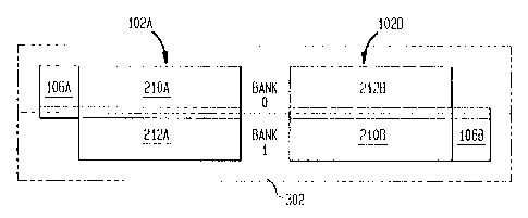
very wide data word. This is illllstr~ted in FIG. 3, in which a DIMM 102A
and a DIMM 102B form a DIMM pair 302. As illustrated, DIMM 102A
;n~ f ~ first memory bank portion 210A, second memory portion 212A, and
first state mGIllol~ 106A. Simil~rly, DIMM 102B in~ lud~s first memory bank
portion 210B, second memory bank portion 212B, and second state memory
106B.
In this implement~tion, first memory bank portion 210A and second
memory bank portion 212B form a first memory bank, labeled bank 0. State
information for data stored in bank 0 is ~ in~;.ined in state memory 106A.
Second ..le ..~l~ bank portion 212A and first IIIGII101,~/ bank portion 210B form
a second memory bank, labeled bank 1. State memory 106B is configured to
store state information co~lc~onding to data stored in memory bank 1. As
cus~d in further detail below, a bank select signal is used to select one of
bank 0 or bank 1 for data access oEY ~ti- n~. Memory bank 0 and memory bank
1 share common address and data lines.
The DIMM of the invention can be produced with a variety of difr~ nt
data storage c~3cities~ In a first prGffll~d f;",bo~;...ent, DIMM 102 has a
thirty-six (36) IllegdbyLG data storage capacity (inc~ ing 32 Illegal~yles of data
and 4 mega~y~s of ECC) and a two (2) megaby~e state information storage
capacitv. This çm~im~nt yields a DIMM pair having sixtv-four (64)
Illega~ Gs of data storage capacitv, eight (8) mc;ga~y~s of ECC, and four (4)
2~ 7~2
megabytes of state info~ ;t n storage capacity. In a second embo limPnt,
DIMM 102 has a ~.~ two (72) megabyte data storage capacity (inc~ ling
64 ",eg~s of data and 8 megabytes of ECC) and a four (4) megabyte state
il f,..--;~ n storage capdcil~. This e~ yields a DIMM pair having one
S hundred twenty-eight (128) ",egab~s of data storage capacity, sixteen (16)
megabytes of ECC, and eight (8) ",egab~s of state infol",alion storage
capacity.
IV. De~ils ofthe DIMMInterroqqe~ts
FIG. 4 is a block .l:~&.i.... ill..~h;.l;~g in~l~nn~!;on of the co"-l)onc
used to implement a DIMM 102 in accor~ance with the first plt;fe~
embo~im~nt of the invention. Data memory 104 is impl^mPnt~d using a
plurality of ~nchronous, dynamic, random access memory (SDRAM) chips
D0-D17. SDRAMs D0-D8 repr~nt memory chips of first memory bank
portion 210, while SDRAMs D9-D17 replesent memory chips of second
1~ memory bank portion 212. In this 32 ,-,egab~ embo lim~ont of DIMM 102,
each SDR~M D0-D17 is a two megabit by eight bit (2M x 8) SDRAM chip.
Thus, each memory bank portion 210,212 is two (2) megabits deep by seventy-
two C72) bits wide, yielding a total data capacity for data memory 104 of four
(4) megabits deep by seventy-two (72) bits wide (i.e., 64 bits for data and 8
bits for ECC). State memory 106 is imple .. l~n~ using a single one megabit
by sixteen (lM x 16) bit SDRAM chip.
Each DRAM chip D~D17 provides an 8-bit data word. To
accomm~te comm~mi~tions with each SDRAM, data path 110 provides an
8-bit data path DQ. As in-li~t~, one chip from each of ~e~O~ bank portions
2~ 210,212 is CQnn~1f~d to an 8-bit data path DQ. For eY~mp'c, SDRAM D0 and
SDRAM D9 are both conn~t~ to DQ[7:0]. Which chip is actually active on
6 ~ 2
-18-
the data path is ~1~ t~- ...in~d by an e~tern~l chip or bank select signal (~
below).
Address and control buffers 214,216 receive 2~bits of address and
control signals, labeled A[l9:0], buffers the address and control ~ig~ , and
provides the address and control signal to SDRAMs D0-D17 as follows.
Address and control buffer 214 provides address and control signals (i.e., row
address strobe, column address strobe, write enable and data mask) to left sidesof bank portions 210,212 (i.e., SDRAMs D0-D3 and D9-D12) via bus 113.
In a~lliti~n~ address and control buffer 214 pIovides a bank select signal (CS0~and a clock enable signal (CKE0) to both the left and right sides of first bank
portion 210 (i.e., SDRAMS D~D8) via lines 117.
Address and control buffer 216 provides address and control signals
~l.e., row address strobe, column address strobe, write enable and data mask)
to right sides of bank portions 210,212 (i.e., SDRAMs D4-D8 and D13-D17)
via bus 115. In ~(ltlitinn~ address and control buffer 216 provides a bank select
signal (CSl~ and a clock enable signal (CKEl) to both the left and right sides
of second bank portion 212 (i.e., SDRAMS D9-D17) via lines 119. Address
and control signals A[l9:0] are described further below in Table 1.
Clock driver circuit 218 provides clock signal 222 to each of SDRAMs
D0-D17 and to the SDRAM of state memory 106. Clock driver circuit 218
generates clock signal 222 based on clock control signals C[5:0]. The clock
control signals C[5:0] are ~le~rihed in further detail below. The data path 114
and address and control path 116 of state memory 106 are ~ Stl~t~ by lines
DIR DQ[15:0] and B[17:0], respectively. These signals are also described in
further detail below.
The72megabyte e~"l~ "~nl of DIMM 102isdepictedinFIG. 5. In
this e l-bod;~ nl~ rather than using ~ight~n two megabit by eight bit (2M x 8)
SDRAMs, the DIMM is imp'~ nlo.nt~ using thirty-six (36) four megabit by 4
~1 7~4~
-19-
bit (4M x 4) SDRAMs. To ?'`f~O~ e the additional chips, a second circuit
board 500 is used. Fight~n of the 4M x 4 SDRAMs (DO D17) are mounb~d
on a first circuit board 103. The other eighb~n 4M x 4 SDRAMs (D18-D35)
are mounted on second circuit board 500. Circuit board 500 is lllounted on
circuit board 103 in a piggy-back f~ ion OII1Y circuit board 103 in~ cle~s
edge con~tor 108 (not shown in Figure 5). All e1~tri~l conn~f;~n.~ to the
SDRAM chips of circuit board 500 occur l~llough the edge c~n~ r of circuit
board 103. Signals are shared by the two boards using a plurality of
i.l~l~onn~ g pins. Each end of each pin is located in a plated through hole
to provide e1~tri(~l conn~ion~ ~t~. the boards. These pins also
physically attach the second board to the first board. An example of a piggy-
back ...o,.n'~d circuit board (not using plated through holes) is provided in U.S.
Patent No. 5,200,917 to Shaffer et al.
In this e~ nl, first memory bank portion 210 is formed from the
front side of each of circuit boards 103,500. For example, SDRAM chips D0-
D8 and D27-D35 can be used to illlplc~nent first memory bank portion 210.
Simil~ly, the back side of e~ch circuit board 103,500 can be used to implement
second memory bank poreion 212. This inr,l~des, for example, SDRAM chips
D9-D17 and D18-D26. The chips on each circuit board 103 and 500 include
on-board c1~1~ing and buffering via clock drivers 218A,218B and address and
control buffers 214A,214B,216A,216B. However, in this embo~iment) each
SDRAM chip is coupled to a 4-bit data path rather than an 8-bit data path.
Thus, a ooll~onding SDRAM chip from each board is used to form the 8-bits
provided by a single chip in the 36 megabyte DIMM. As in the 36 megabyte
DIMM embodiment of FIG. 4, all SDRAM chips D0-D35 are addressed
~imu~ . A bank select signal (one of signals A[l9:0]) is used to select
belween memory bank portion 210 and memory bank portion 212.
2 1 ï 66~2
-20-
V. DIMM Chi~ yout
A plc;r~led impl^mentqtiot~ of the 32 megabyte DIMM embodimPnt is
depicted in FIGs. 6A and 6B. FIG. 6A shows front side 202 of DIMM 102.
FIG.6Bshowsbackside204ofDIMM,102. Inthis~ r~,ledimple~ ntqtiQn,
S circuit board 103 is apploAimately 1.34 inches high by 6.6 inches long and
in~lud~s a 122 pad long by 2 pad wide edge cQIln~or al,ong one longitu-1inq1
edge of the circuit board. SDRAM,s D0-D8, SDRAM, DIR0 (for state memory
106), data and control buffers 214A and clock driver 218A are mounted on the
front side 202 of circuit board 103. SDRAMs D9-D17 and data and control
buffer 216A are mounted on the back side 204 of circuit board 103.
FIGs. 6A and 6B are lc~l~nt~ e of the 72 megabyte embodiment of
the invention as well, as the 32 megabyte embodiment with the following
dirr~ ces. First, in the 72 ",eg~rle embo~im~ont, SDRAMs D0-D17 are 4M
x 4 devices instead of 2M x 8 bit devices. .Se~ond, the di-eclol~ memory chip
(indicated as DIR 0) is a 2M x 8 bit device instead of a lM x 16 bit device.
Third, in the 72 megabyte embo~liment, a second 2M x 8 bit SDRAM chip
(in~ir-q-ted by dashed lines in FIG. 6B as DIR 1) is used with DIR 0 to
implrnPnt state memory 106.
A p-efclIed implcmentqtion of the piggy-backed second circuit board
500 of the 72 megab~le DIMM embodimPn~ is depicted in FIGs. 7A and 7B.
FIG. 7A shows a front side 702 of second circuit board 500. FIG. 7B shows
a back side 704 of second circuit board 500. In this prer~d i."l)le~ nl~l;on,
circuit board 500 is approsim~tPly 1.16 inches high by 6.6 inches long and
;ncl~d~,s 116 in~l~nl-~ting pins (not shown) providing el~tri~l co~nections
with circuit board 103. SDRAMs D18-D26, data and control buffer 214B and
clock driver 218B are mounted on the front side 702 of circuit board 500.
SDRAMs D27-D35 and data and control buffer 216B are mounted on the back
side 704 of circuit board 500.
~ i 7~642
Vl. The Pad Descn~tion
Table 1 lists the pad name and fun~tionc for the edge connector's pads
accolding to a pl`~f~l~ çmho~lim~nt of the present invention. The left-hand
column lists the abbreviated pad names and the right-hand column lists the
S function of the pads listed in the ~ tPd row of ~e table.
Table I Pad Descnption
Pad Name ~bnction
A[ll:Or DataMemory Address (Row:AllO:Ol; Col:A[9:0]; Bank select: All)
DQ[71:01 Data VO Pads for Data Memory
CSl, CS0 ~ Chip select for Data Memory SDRAM~
RE A Row address strobe (RAS) ~ ' for Data Memory
CE A Column addresD strobe (CAS) ~ ' for Data Memory
WE ~ Write enable c ~ ' for Data Memory
DQMA Input/Output mask for Data Memory
CKEl,CKEOA Memory clock enable for CSl and CS0 SDRAM's ~;D~ti~
DIR A[11:0]' State Memory Address (Row:A[10:0]; Col:A[7:0]; Bank select: All)
DIR DQllS:O] Directory data I.e., state i,.ru~ ~ ) VO for State Memory
D~ CS B Directory chip select for State Memory
DIR REB Directory row address strobe c ' for State Memory
DIR CEB Directory column address strobe ~ ' for State Memory
DIR WE 8 Directory write enable - - ~ ' for State Memory
DlR DQMB Directory inputloutput mask for State Memory
DIR CKEB Directory clock enable for State Memory
PCLK, PCLK c Dil~.~ ' LVPECLclock inputD
TCLKC LVTTL clock input~D
TCLK SELC Selects TCLK when hiBh and PCLK when low
PLL ENC Enables PLL on clock driver
PLL CLRC PLL re~Det and tri-state clock driver outputs
~ 1 76642
-22-
Table I Pad Descnp~on
Pad Name Function
V3 Power 6upply (3.3VD.C.)
GND Ground
SI~RIAL DAT Line to read content6 of 6erial prom
A= The6e pad6 are shown collectively on FIGS. 4 and 5 a6 A119:0]
B= These pads are shown coll~li~l~ on FIGS. 4 and 5 as B[17:0
c= These pad6 are ~hown collectively on FIGS. 4 and 5 a6 C[5:0]
The first pad desc,i~tion is for the address pads and is abbrt;viated
Atll:O]. During row addressing the eleven least ~ignifi~qnt bits are used.
During column addressing the nine least ~ignifi~qnt bits are used in the 36MB
DIMM embo limPnt and the ten least ~ignifi~qnt bits are used in the 72MB
DIMM Pmk~imPnt The most ~ignificq-nt bit (All) is used to select between
internal SDRAM banks. ~hese "inten~al banks" are dirf~.el~t banks than banks
ze~o and bank one of SDRAM DIMM 102 de.~ibed above. Therefore, banks
ze~o and one will herearler be ler~l~d to as ~Yt~rnqln banks that are selected
1~ via PYt~mql back chip select signals CSl and CS0, to distinguish them from the
"internal SDRAM bank select" signal Al 1. This naming convention applies for
SDRAMs used for data, as well as those used to store state information.)
Data is input to, and output from the data memory of the SDRAM
DIMM via 72 data input/output (I/O) paths abbreviated DQt71:0]. Since the
SDRAM DIMMs are used in pairs, a single access of the data memory on a
single DIMM provides 72 bits, which when c~nc~ten ~ with 72 bits of the
paired DI~I, yields a 144 bit data word that includes 128 bits of data an 16
bits of ECC.
There are eight lc -qining paths for the data memory of the SDRAM
2~ DIMM. Two PYtPrnql bank chip select pads abbreviated CSl and CS0_, a
-23-
row address strobe co..----and pad abbreviated RE_, a column address strobe
c4----nal d pad abbreviated CE_ and a write-enable co--.---and pad abbreviated
WE are standard signals used for s~1~tin~ addl~,ng, and write-enabling
SDRAM chips, as would be app~l~t to a person skilled in the relevant art.
Similarly, two pads are provided for ~ne~-o~ clock enable for the two banks
of SDRAMs, lGs~ec1i~ely, and are abbreviated CKEl and CKE0. A single
input/output mask path is also provided, and is abbreviated DQM. The
function of the DQM mask pad will be described below in conn~tir,n with the
waveform diagrams.
The pads for the state memory of the SDRAM DIMM will now be
des~ribed. The collection of d.reclol~ address pads are abbreviated
DIR A[ll:0]. Row add ess-ng for the state me Wly uses dif~;l~l~ address bits
AtlO:O] and column addressing utilizes dir~ address bits A[7:0] for a
32MB DIMM and bits A[8:0] for a 72MB DIMM. A twelfth d~clol~ address
1~ pad (Al 1) is used for internql SDRAM bank sel~tir,n
Sixteen bits of state h~fol---ation is provided by dhec~l~ data I/0 pads
abbreviated DIR DQ[15:0]. The next five pads listed in Table 1 have similar
fimrtirnqlitirs as de~ ;l ed above in conn~-~;on with the analogous paths for the
data Ill~;lll~l~ section of the SDRAM DIMM. The dilcclol~ chip select pad is
abbreviated DIR CS . A directory row address strobe command pad is
abbreviated DIR RE . A dil~ctol~ column address strobe co------and pad is
abbreviated DIR CE . A dLect~,~ write-enable c4---,--and pad is abbreviated
DIR WE . A lL~l~ input/output mask pad is abbreviated DIR DQM. An
~rlitionql dil~clol~ clock-enable pad, abbreviated DIR_CKE, is provided for
enabling the state memory clock.
According to a pfer~lled embodiment of the present invention, a
Motorola, Inc., (Phoenix, ~ri7011q) MPC931 PLL chip, is used as a clock
driver circuit. l~ ~ this specific in~ ed circuit ~ pOl~ both low voltage
6 4 2
-24-
tr~ncictQr-tr~nci~tor-logic (LVTTL) or low voltage positive emitter coupled
logic (LVPECL) lcsp~li~ely, the SDRAM DIMM of the present invention can
include pads to f ^i1it~te either type of logic level for the clock driver circuit.
T~.~c;r~,le, dirre~c"lial LVPECL clock pads abbreviated PCLK and PCLK_ are
provided. ~d~lition~11y, a LVTTL clock pad abbreviated TCLK is also
provided. To select b~ ~n the two possible power pad inputs, a select pad
ab~l~vialed TCLK SEL is provided. The logical voltage value applied to the
TCLK SEL pad will select which voltage pads that the clock driver circuit will
use. For eY~mp1e, the TCLK can be se1ect~ when the TCLK_ SEL pad is a
logic high and the PCLK pad can be used for pUW~ the clock driver circuit
when the TCLK_SEL pad is at a low logic level. Another pad enables the
phase lock loop portion of the clock driver circuit, and is abbreviated PLL EN.
Reset and tri-state clock driver circuit outputs for this m~n11f~cturers' chip can
be SP1~tP~ via another pad abbreviated PLL CLR. Other suitable pad
~l~u~ge,l,ents using functionaUy similar PLL (phase locked loop) chips would
be ap~ent to a person skilled in the relevant art.
A power supply voltage (e.g., 3.3 V.D.C.) and ground are supplied via
pads abbreviated V3 and GND ~s~eclively. If imrementPd, a single
a~ ition~l pad is used to read the cQ.,'~nl~i of the serial pç~gla"""able read-only
Illelllol~ (PROM), which is labeled SERIAL DAT.
FIG. 15 i11~ 'f~ a preferred eYçmp1~ry pad ~ccignmpnt for the entire
244 connector pad edge connpctor 108. This figure is broken-down into 6
mnc in order to show all 244 pad ~ccignmPntc on a single page. 14 pads
are un~Ccignp~ Each column shows the pad number ~Ccignmpnt followed by
the abbreviation of the pad description col,e-sl on~ing to the pad narnes listedin Table l. The pad ~ccig~ are made tal~ng trace lengths on the PCB 103
into consideration to minimi7~ signal skew and loading.
~ 1 766~2
-25-
VII. l~ming Requirements
Table 2 shows rep~ ;./e timing IG~1Ui1GIIIen~S for an eYemplq~y
SDRAM DIMM pair using NEC Co~ t;r~n (Japan) part ~.~....h
uPD4516421GS-A12-TJF (4Mx4), uPD4516421GS-A12-TJF (2Mx8) or
uPD45161GS-A12-TJF (lMx16). The timing lc~ .llGIlls listed in Table 2
are for nomi~ql ~ 'J~eS bGl~n O and 70C and a power supply voltage
of 1~LWG~1l 3.3 volts and 3.6 V.D.C., wi~ all clock references to PCLK. The
~ming r4uilGIl~Gll~ of Table 2 include clock jitter and skew of approAil~alGly
1.5 n~qnos~oll~ls
2 1 7664~
-2
Table 2 Ifming Requirements
(Ta = 0 to 70C, VDD, VDDQ = 3.15VDC to 3.6VDC)
AU clock ,cf~ (Ref) are to PCLEC.
The timings include a clock jitter + skew of l.5ns max
1. Clock cycle time = 20ns max
2. Clock to data in setup = 4.5ns min
3. Clock to data in ho1d = 2.5ns min
4. Set up time input address = 12.0ns min
5. Hold time input address = l.Ons min
6. Set up time input c ' = 12.0ns min
7. Hold time input ~ ' = lns min
8. Access time from clock (CAS latency = 2) = l5ns max, load 80pf
9. Hold time output data = l.5ns min
10. Clock to data out, high ;-- peA~ ~e = 16.5ns max, load 80pf
1~ 11. Clock to CKE setup (power down exit) = 12.0ns max
12. Clock to CKE hold = l.Ons min
13. Ref/active to Ref/active c ' period = llOns min
14. Active to p,~ch~L_ ^ ' period = 75ns min - lOOOOns max
15. Active c ~ ' to column c ' (same bank) = 38ns min
16. PI~L~ge to active c ' period = 38ns min
17. Last data in to p.~ e lead time = 18ns min
18. Refresh period = 64ms max
The timing p~ shown in Table 2 generally lep~esent time
periods as measured at the edge conn~tor~ ignoring any small effects the
conn~tor itself will have on the signals. These times would appear diLrer~l t
if measured at a location on the SDRA~s th~m~ ves. The row and column
addresses are set by a memory system into which the SDRAM DIMMs are
~ t8~
conn~ted and as l~uilæd by the ~-ific SDRAM devices employed on the
DIMMs.
VlII. Wal~efoml Diagrams
The timing ~iqgr~mc for reading and writing inroll.ldlion for the
S SDRAM DIMM are shown in FIGS. 8-13. FIG. 8 shows a r~læse~ ;ve"data read" timing tli~ram acco~-ilg to the present invention. FIG. 9 shows
a lc~ ive "data write" timing d;~.~ -- acco~ling to the present invention.
FIG. 10 shows a læ$l~ ;ve "read modify write" (RMW) timing ~li~r~m
acco~iing to the present invention. The vertical bars ~æ~r~sent clock edges, at
which the control and address signals are sampled by the SDRAM parts.
Turning now to FM. 8, a total of six timing traces are il1ustr;~te,
including: chip select (CS~ 802; row address strobe (RE~ 804; column
address strobe (CE~ 806; write-enable (WE~ 808; address (A) inputs 810;
and, data (DQ) inputs/outputs 812.
1~ The SDRAM DIMMs data output 812 l~leserlt~ the timing of an output
bascd on ~pli~ti~n of the row and column addresses and assertion of the RE,
CE and WE control signals. The data memory is arranged so that a single
row access can be followed by four column addresses (C0, C2, C4 and C6) to
access a block of data from a DIMM pair. A block of data (not including
parity/ECC data) is 8 words by 16 bytes, or a total of 128 bytes (which is 64
bits per DIMM or a total of 128 bits per location access, since the pair is
~c~d in parallel). So for 4 c~n~cutive location ~ s~s per RA, a total of
8 data words D0-D7 by 16 bytes are output. Similarly, the SDRAM DIMM
pair is written to in block writes as illu,l.~t~ by trace 902 in FIG. 9. Table
3 shows lc~ /e cycle latency for various timing p~r~mPters of FIGs. 8-
10. These parameter l~tPn~ies are listed in n~no~cond and are nominal.
2 ~6~4~
-28-
Table 3 Cycle L~ztency at SOMHZ
1. CAS latency = 2 (number of clock~ between CE c ' and data i8
2. tRCD = 2 ( number of cloclc~ betwe~en Rl~ and CE
3. RAS latency = 4 ( number of cloclcs between R~ and data i~ ' ' ' e).
4. tRC = 6 ( number of cloclcs betwe.en refre~h and Rl~
5. tRAS = 4 ( number of cloclc6 between R~ and ~ ' `a-
6. tRRD = 2 ( number of clock~betweenRE ~ ' )
7. tRP = 2 ( number of cloch between p~ ' ~- g and RE c ~ d).
8. tDPL = 1 ( number of clock~; betwe(en data in and l"~h~,,- E ~ a).
9. tDAL = 3 ( number of cloclcs betwe~en data in and Rl~ for ~ ~ ~J ~,~e.).
Read modify writes can also be done on data, as shown in FIG. 10. A
location is ~c~-c~ by a single RE and CE (traces 1002 and 1004
l~ti~rely) and the data is read at the first D0/Dl pair 1006. After the data
is m~lifif~d it is written back as shown by the second D0/Dl pair (1008) to the
DIMM pair by asserting the CE and the WE (trace 1010) signals.
As noted above, the state memory is ~e-~ in parallel with the data
memory. A state memory compri~s two reads and two writes, since each
dil~;ctul~ entry is 32 bits wide, and each state memory in the prer~.led
embodiment implc-nPnt~ SDRAMs that are only 16 bits deep. Also, page
migration incremPnting r~ui~c reading the location that co~ onds to the
block being ~ ~d for both the node making the request and the home node,
and a write to increment the count for the node making the request. The page
.,.;~"i-~;. n counts ke~p track of the number of times a node ~r~sses a particular
page of memory. Thus, that count must be incr~ ..ent~ each time a page is
~cc~ss~ If the count for some node ~cc~ssing a given page eY~e~s either a
pledet~- .,. n~d threshold or the count for the requestor minus the count for the
home node eYceeds another threshold, the page is migr~t~d to the memory
2~76b4~
-29-
q~sori-q-t~ with that node. A more ~lrt-qiled description of page migrtq-tion isfound in the co~ di~g q~li~qti- n (Attomey Docket No. 1452.0690000) noted
above. Thus, during the 8 cycle read or write of the data memory, the
coll~pon~ing state memory is read a total of 4 times and written to a total of
3 times, so that ncc~ s to the data and state info.. ~;on iS b-q-lqn~
FIGS. 11, 12 and 13 show three s~~ e wavefoll~l diagrams involving
data ...~ ;ng, inclll-l;ng reads, writes, and revisions, l~c~iv-ely. In FIG. 11
the following signals are shown: chip select (DIR_CS~, row address st~obe
(DIR_RE~, column address strobe (DIR_CE~, write enable (DIR_WE~,
inputloutput data masks (DIR_DQM), address A inputs and data (DIR_DQ)
input/outputs. The dileclol~ cycle for a read st~rts by reading the first half of
the di~ word (D0), the page migration count for the r~u~ling node (S),
the second half of the directory word (Dl), the home node's page migrtqtion
count ~H), then after a dead cycle on DIR_DQ, the new page migration count
1~ (S) and the new di~ olr inform~qtion (DO and Dl) are written into the state
memory. The information is read out in the listed order due to l~uilt;menls
of the memory controller that lead to the quickest IIICII101,~ respon~e time.
FIG. 12 is a slight pcll-~u~lion of the wavefolllls shown in FIG. 11.
The order of S and D0 are ~vilched in this figure in contrast to FIG. 11.
FIG. 13 shows the state access for a state revision operation, which is
a state-only access and does not require a memory access. To minimi7e the
overhead of these revisions operations only the dL~ o,~ inf rmqtinn is
~q-rce~.~d
~ 1 76642
-3
Xl. Expanded State Memory
When used in a DSM mulli~ ssor, the DIMM pairs of the invention
are used to implPmPnt main memory. Each p~ r node of the DSM
mulli~ inrly~e$ a portion of main memory. In the 36 megabyte and 72
S megabyte embo~imPntc of the DIMM, the state memory config~lrrqtionc
diccuss~Pd provide suffir;Pnt capacily to 9q^C4"~ P- the state info~ ;Qn
required for a system having 16 nodes. For e~mrle, each state memory
descrihPd above includ~ps 16 bit wide words of state inro~ ;on.
When the number of nodes eY~ 16, ~-litionql state memory is
l~uir~d at each node to accommodate more state inÇol"lalion about caching,
because more cache mpmoriprs are likely added to the system. The ~ iti~nql
state memory can be provided by using a state memory-only DIMM.
According to a prer~,led embo~imPnt of this aspect of the present invention,
~is state memory-only DIMM adds 32 bits of additional state memory. The
resulting total state Illelllol~ provides 48 bit wide words of state inro""ation (16
original bits on the SDRAM data/state memory DIMM plus 32 bits from the
state memory-only DIMM). With the q~l~litionql state memory, the DSM
mullil?~cess~r can acco..~...~'P up to 64 nodes using conventi-nql bit-vectors
and up to 512 nodes using fleAible dil~;~ly bit vectors. The spPcific numbPr
of additional state informqti~ n bits c. n vary and is eYtPn~-q-hle, as would beappal~nt to a person of ol.lin~y skill in the relevant art.
The orgq-rli7-qtion of DIMM pairs 302 and state memory-only DIMMs
1406 in a main memory portion 1400 of a node of a DSM multiprocessor is
illust~ated in Figure 14. A Illelllol~/d,l~h.l~ controller 1402 at the node of the
DSM mul~l~,cessor pelroillls all memory mqnag~om~nt fun~tion~ for the data
and state memory on the DIMMs 302 and 1406. A memory address and
control buffer 1410 buffers all address and control lines 1420 going to the datamPmori~s of the DIMM pairs 302 from the controller 1402. A state (di~
6 ~ ~
-31-
address and control buffer 1412 buffers all address and control signals on lines14æ going to the state memorip~c of the state memory-only DIMM pairs 1406
from the controller 1402.
Each state Illelll~l~-only DIMM 1406 can be impl~ l~ using a single
PCB. The PCB can be populated with SDRAM chips of similar or ~iccimilqr
capa ;ily chips as the SDRAMs of the DIMMs 302. The SDRAMs of the state
"~G ,~l~-only DIMMs 1406 are Gr~ni7~ with two banks of state memory so
that state inro~ nn and addressing of the state informqtion is concict~pnt with
the d-lccl~ (DIR)/state mPmoriP~c on the DIMMs 302.
A bus eY~ g~ l 1408 passes the 144 bit data word to/from each DIMM
pair 302 via bidire~tinnql buses 1409. The bus eY~ qngP~ 1408 takes 144 bits
data at the memory speed and converts it to 72 bits at twice the memory speed.
In a plGfc~lGd ~,llbo~ -l the bus eYrllqnger 1408 is imp~ nl~d with a part
llUlllber SN74ALVC16282 (~ --Jr~-~---Gd by Texas In~u...en~, Dallas Te~L)
that converts 144 bits at 50 MHz to 72 bits at lOOMHz, and vice versa for
bidirectionql transfer of the data bel~ the DIMMS 302 and the controller
1402, via bidi~Gclollal bus 1411. Di~ data is not burr~iGd, and is
transferred bGlwee,l the state memory-only DIMMs 1406 and the controller
1402 via bidirectional bus 1424.
For pù,~os~s of illustration, a 36 megab~le embodiment and a 72
megabyte embo~1imPnt of the DIMM have been descri~ed. It should be
understood, however, that the DIMM of the invention may be produced in
other data c~itips~ For eY~mpl~, using 64 ,-,ega~it (i.e., 8M x 8) SDRAM
chips, a single board DIMM may be produced having 128 megab~ le data and
2~ 16 megabyte ECC (18 chips x 8 megabytes per chip) storage capacity
(including data and ECC). This would yield a DIMM pair having 256
mega~s of data storage capacity. If a piggy-back bo. rd is used as in the 72
",egal)~ DIMM e",boli 1ll.~ de~ ;I,ed above, the 64 megabyte SDRAM chips
~I f ~6~
-32-
can be used to ir, '^ nPnt a 256 I,lega~le data and 32 megab~ ~ ECC DIMM
and a 512 megabyte data, 64 Illegab~le ECC DIMM pair.
In the pref~l~xl embodiment described, a piggy-back board is used to
a11ow the DIMM to ;lc~l...~ 'A 36 SDRAMs for the data memory. A person
skilled in the art will l~c~ni~P that chip st^^tin~ techniques may also be used
to accolllll-odate 36 SDRAM chips. If chip st^^l~i~ techniques are used, the
piggy-board may be e~ 'ed
~ 1t~nAtively, 4 ...P~,a~;l (i.e., lM x 1) SDRAM chips can be combined
to produce DIMMs with lower storage capacity, or the above-described
0 ~ t;~ and /or piggy-back t~P~hni~ Ps can be used for higher storage capacity.
X. Conclusion
While various ~ bo~ of the present invention have bcen described
above, it should be understood that they have been pr~nted by way of
e~ample, and not limit~tir n, It will be app~.-t to pel~l s skilled in the
r~levant art that various ~h~e-~ in form and detail can be made therein without
de~L-g from the spirit and scope of the invention. Thus the present invention
should not be limited by any of the above-described exemplary emb~imPnt~,
but should be defined only in accoç~ance with the following claims and their
equivalents.