Note: Descriptions are shown in the official language in which they were submitted.
21766~6
Broadband Circularly Polarized Dielectric Resonator Antenna
Field of the Invention
This invention relates to dielectric resonator antennas for use with circularly polarized radiation
and more specifically to such an antenna with a single feed.
5 Background of the Invention
The increase in use of satellites in communication and navigation systems requires small
antennas for vehicular (car, boat or aircraft) applications. These small antennas must be able to
receive circularly polarized radiation even from low elevation angles.
An antenna element in common use today is the microstrip patch antenna which inherently has a
10 very limited frequency bandwidth. This antenna has numerous advantages such as simple
fabrication, conformal planar structure, and the existence of many well proven design
methodologies and tools. Satellite communications antennas have been built using microstrip
patch antennas having metallic radiating elements and producing circularly polarized radiation.
In U.S. patent 4,843,400 a microstrip patch antenna is disclosed which produces circularly
15 polarized radiation using a single feed. The antenna is based on a symmetrical patch with
differing dimensions along the axes; however, as many of the existing methodologies and tools
have been designed for microwave bands, use of millimeter wave bands requires new antenna
design methodologies.
At higher frequencies, metal radiating elements, such as those present in microstrip patch
20 antennas, develop large ohmic losses in conducting surfaces and their effects become significant,
also dielectric substrate materials become increasingly dispersive. Designs can not simply be
scaled from lower frequencies to higher frequencies without accounting for these factors. Other
21 76656
traditional approaches include the use of multiple monopoles with a reflector and helical
antennas both of which have been found to lack robustness and to be difficult to fabricate.
Unshielded dielectric resonators are known to radiate strongly at and around some of their
resonant frequencies. Dielectric resonators possess inherent advantages such as high radiation
5 efficiency due to no conductor loss, small size and mechanical simplicity. The radiation pattern,
resonant frequency and the operating frequency bandwidth of a dielectric resonator antenna
depend on the excited resonant mode, permittivity, the resonator geometry and its surroundings.
These provide many degrees of design freedom which may be exploited in controlling antenna
characteristics .
10 Rectangular dielectric resonator antennas have been excited in "magnetic dipole" mode and
shown to produce a linearly polarized electric field. To achieve this, a rectangular dielectric
resonator antenna is placed on a metallic plane over a small aperture which is excited by a
microstripline on the other side of a dielectric substrate. This can also be done using a single
probe or monopole antenna placed near the centre of one side of the resonator. The rectangular
15 resonator, and its image in the ground plane combine to form an isolated horizontal magnetic
dipole.
If a single element is to be implemented in arrays, the simpler the single-element feed, the
simpler the array feed. The limiting case would be a single-feed antenna. It is desirable to
minimi7e the complexity of an antenna feed network so that losses and physical size are
20 lessened. Producing circularly polarized radiation requires two fields mutually orthogonal in both
space and time having equal amplitude. Thus, to modify an inherently linearly polarized antenna
element (such as the dielectric resonator) such that it is circularly polarized, requires the
excitation of two mutually orthogonal modes within the antenna element. This can easily be done
with dual feed points, or with an array of properly designed linearly polarized antenna elements.
25 It has now been found that the generation of circularly polarized radiation using a single feed and
a single dielectric resonator can be accomplished.
21 7~656
Object of the Invention
It is an object of this invention to provide a single feed dielectric resonator antenna for use with
circularly polarized radiation.
Summary of the Invention
In accordance with an embodiment of the invention there is provided a radiating antenna
compnslng:
a) a dielectric resonator antenna having a bottom surface and outer surfaces and designed to be
capable of being excited in two orthogonal modes simultaneously;
b) a single feed means capable of exciting two orthogonal modes simultaneously;
whereby the feed means and the dielectric resonator operate in conjunction to simultaneously
excite two mutually orthogonal modes in the dielectric resonator.
In accordance with an embodiment of the invention there is further provided a radiating antenna
comprising:
a) a single feed means further comprising
i) a dielectric substrate having a conductive coating on an anterior side thereof and with
an opening having unequal dimensions along two perpendicular axes coplanar with the
dielectric substrate, and
ii) a microstripline on a posterior side of the dielectric substrate disposed to cross the
opening along the centre and parallel to the shorter of the unequal axes; and
c) a dielectric resonator having a bottom surface, outer surfaces, and a length and width disposed
on the conductive coating over the slot and further disposed such that an axis of the dielectric
resonator is at an angle of substantially 45 degrees to the axes of the slot.
21 i6f~56
Brief Description of the Drawings
Exemplary embodiments of the invention will now be described in conjunction with the
following figures in which:
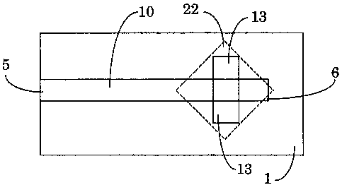
Fig. 1 is a bottom view (not to scale) of a dielectric resonator antenna element according to this
5 invention with elements on the top side shown with dashed lines;
Fig. 2 is a profile view (not to scale) of a dielectric resonator antenna element according to this
invention wherein a microstripline and a slot form feed means;
Fig. 3 is a profile view (not to scale) of a probe fed antenna element according to this invention
wherein a feed probe inserted into a dielectric resonator forms feed means;
10 Fig. 4 is a top view (not to scale) of a further dielectric resonator antenna element according to
this invention wherein a feed probe inserted into a dielectric resonator forms feed means;
Fig 5 is a profile view (not to scale) of a probe fed antenna element according to this invention
wherein a probe in contact with an outside edge of a dielectric resonator forms feed means;
Fig. 6 is a top view (not to scale) of a probe fed antenna element according to this invention
15 wherein a probe in contact with an outside edge of a dielectric resonator forms feed means;
Fig. 7 is a profile view (not to scale) of a further probe fed antenna element according to this
invention wherein a probe inserted into a dielectric resonator forms feed means; and
Fig. 8 is a top view (not to scale) of a further probe fed antenna element according to this
invention wherein a probe inserted into a dielectric resonator forms feed means.
21 7~656
Detailed Description of the Invention
Referring to Fig. 1 and Fig. 2, an antenna is shown comprising a large substantially flat dielectric
substrate 1. A top side of the dielectric substrate 1 is coated with a conductive film 8 and above
this is located a dielectric resonator 22 shown in dashed line. Through the conductive film 8 and
5 the substantially flat dielectric substrate 1, a feed means in the form of a transverse narrow slot
13 having a long axis and a short axis, in the form of a rectangle, is formed. The slot may, for
example, be formed by conventional etching. A microstripline 10, shown in solid line in Fig. 1,
is formed on a bottom side of the substantially flat dielectric substrate 1. The microstripline 10
extends from an input/output 5 disposed at an end thereof, passing under the centre of the long
10 axis of the narrow slot 13 and termin~ting a fixed distance after the narrow slot 13. The
microstripline may be moved away from the centre of the long axis of the narrow slot 13 in order
to tune the antenna. Optionally, to the input/output 5 of the microstripline 10 is attached a proper
connector (not shown) to feed energy to the microstripline 10 for transmitting operation of the
antenna or to receive energy from the microstripline 10 for receiving operation of the antenna.
15 The connector type is determined by the requirements of each application. Alternatively, the
microstripline 10 is continued to a further connection; for example, the microstripline may
connect several antenna elements and have a common connector for use in an antenna array.
The dielectric resonator 22 has three perpendicular axes which meet at an origin and which
reflect width, length and height of the dielectric resonator 22. For rectangular solids, each edge is
20 parallel to an axis. For other shapes, the axes are to be defined according to the particular shape
or determined experimentally. In experimentally determining the axes of a particular solid for use
according to this invention, the dielectric should be excited in a linearly polarized fashion using a
single feed. The direction of polarization is a first axis and the excitation point lies on this axis.
For use with the present invention, another axis must exist orthogonal to the first axis. Exciting
25 different points along an outside edge of the solid and following a path from the excitation point
to the another axis, will result in different balances between the two orthogonal fields.
21 76656
The substantially flat dielectric substrate 1 has a thickness which is small compared to the
operating frequency of the antenna. When the antenna is used to transmit, power is fed into the
input/output 5 of the microstripline 10. The power propagates along the microstripline 10, and
the fields associated with the power couple through the narrow slot 13 exciting fields within the
5 dielectric resonator 22. The dimensions of the narrow slot 13 and its displacement with respect to
the microstripline end 6 are optimized so that nearly all of the incident energy is coupled to the
dielectric resonator 22 at its resonant frequency. The dimensions of the narrow slot 13 are chosen
to ensure that its lowest order resonating frequency is much higher than the resonant frequency of
the dielectric resonator 22.
10 The dielectric resonator 22 is placed over the narrow slot 13 so that the length axis of the
dielectric resonator 22 is at an angle of substantially 45 degrees with respect to the long
dimension of the narrow slot 13. The angle may be varied slightly in tuning the antenna to
change the performance characteristics of the antenna. The dielectric resonator antenna 22 is
attached to the conductive film 8. For example, the dielectric resonator 22 can be glued to the
15 conductive film 8 with an epoxy or a silicone compound. This positioning causes two mutually
orthogonal "magnetic dipole" modes of the dielectric resonator 22 to be excited simultaneously.
The directions are parallel with the conductive film 8 and are aligned with the length and width
axes of the bottom side of the dielectric resonator 22.
An antenna was tested wherein a rectangular non-resonant slot with a slot width of <lambda>/20,
20 where lambda represents the guided wavelength within the dielectric, was etched in a substrate
0.0635 cm thick having a dielectric constant of 2.32. The operating *equency range was 4 to 6
GHz. The microstripline feed extended approximately <lambda>/4 past the slot. The dielectric
resonator was substantially cubic with the dimensions chosen such that
fl/Ql + f21Q2 = f2 -f,
2 1 766S~
where f, and f2 denote resonance frequencies and Q, and Q2 denote unloaded radiation Q-factors
of the two modes. Further, the dielectric resonator 22 was glued at an angle of about 45 degrees
relative to the axes of the slot with silicone cement. The resulting rectangular dielectric resonator
had a dielectric constant of 40 and dimensions of 5.8 mm by 6.4 mm by 6.4 mm and the antenna
5 operated between 5.2 GHz and 5.5 GHz. The radiation emitted by such an antenna is circularly
polarized.
Refering to Fig. 3 and Fig. 4, an alternative embodiment is shown wherein the dielectric
resonator 22 is suitably drilled and an end of the feed means in the form of a probe 23 inserted
into the interior of the resonator through one of the diagonals. The probe 23 is isolated from the
10 metal film 8 by a spacing means 123. Typically, the probe is a coaxial cable provided with a
centre conductive element acting as the probe and an outer conductive shield in contact with the
metal film or ground plane. The shield and the centre conductive element are separated by a
spacing means 123. Alternatively, another suitable probe 23 and spacing means 123 may be
used. This preserves many of the benefits of using probe technologies and those of microstripline
technologies. In Fig. 4, the spacing means 123 and the probe 23 are shown in dashed lines to
indicate their presence below the dielectric resonator 22. Positioning of the probe 23 such or in
contact with an outer edge on or near a corner thereof excites two mutually orthogonal "magnetic
dipoles" of the dielectric resonator 22 simultaneously. The two "magnetic dipoles" are parallel
with the ground plane and are aligned with the length and width axes of the dielectric resonator' s
20 bottom side.
An alternative embodiment of the invention, shown in Fig. 5 and Fig. 6, comprises a
substantially flat conducting ground plane 18 provided with an opening designed to receive a
feed means. Through this opening a feed means in the form of a suitably sized conductive probe
23 is placed. The dielectric resonator 22 is affixed to the substantially flat conducting ground
25 plane 18, for example with an epoxy or silicone compound, such that it is in contact with the
probe 23 at or near a corner 19 of the dielectric resonator 22.
2~ 76~6
The probe dimensions are chosen such that a good impedance match is had between the feed line
and the dielectric antenna element 22, but also so that the probe 23 is not resonant at the
frequency of the antenna operation. The probe 23 termin~tes in a suitable connector 20 in the
form of a coax connector on the opposing side of the ground plane 18. The connector 20, for
S example, may be used to connect a suitable feed line from a radio-frequency source. The ground
plane 18 is thick enough to ensure that skin depth at the frequency of operation is exceeded and
the dimensions of the ground plane 18 are chosen to ensure desirable antenna radiation
performance.
In operation, the probe 23 is provided with a signal to be transmitted or provides the received
10 signal through the connector 20 disposed on the bottom side of the conducting ground plane 18.
The probe 23 is spaced from the conducting ground plane 18 by a spacing means 123 of non-
conductive material.
Referring to Fig. 6, the dielectric resonator antenna 22 is shown relative to the probe 23. The
spacing means 123 disposed between the probe 23 and the conductive ground plane 18 is made
15 of non-conductive material. The probe 23 is placed at or near a corner of the dielectric resonator
antenna 22, in the form of a substantially cubic solid, such that both modes are excited
simultaneously. The optimal location is determined experimentally.
Alternatively, as shown in Fig. 7 and Fig. 8, the dielectric resonator 22 may be suitably drilled
and an end of the probe 23 inserted into the interior of the resonator on a diagonal. The probe 23
20 and the spacing means 123 are shown in solid to indicate the presence of the dielectric resonator
22 to the foreground. This positioning of the probe 23 excites two mutually orthogonal
"magnetic dipoles" of the dielectric resonator 22 simultaneously. The two "magnetic dipoles" are
parallel with the ground plane and are aligned with the length and width axes of the dielectric
resonator's bottom side.
21 7~6
The radiation Q-factor of an open dielectric resonator depends primarily on the dimensions and
the permittivity of the resonator and decreases with a decrease in permittivity. Since the
impedance bandwidth of an antenna is inversely proportional to the radiation Q-factor, a
relatively large frequency bandwidth can be obtained by selecting a low value of dielectric
5 constant for the resonator material. Thus, the configuration offers advantages in terms of a
relatively large operating bandwidth over which the antenna radiates efficiently; however, if the
application requires a lower impedance bandwidth, this can be achieved by selecting a higher
dielectric constant. This would also further reduce the size of the antenna, since the wavelength,
within the dielectric (guided wavelength) is shorter than the equivalent free-space wavelength.
10 A dielectric resonator antenna, such as those shown in Fig. 3, Fig. 5 and Fig. 6, using an edge
feed of a dielectric resonator 22 with almost equal length and width dimensions generates
circular polarization when the ratio of dimensions is properly chosen. Circular polarization
occurs because the different dimensions allow two spatially orthogonal modes with slightly
different resonant frequencies to coexist. When the proper frequency spacing is chosen between
15 the modes, they exist in phase quadrature. This inter-mode relation can also be obtained through
the use of inductive or capacitive discontinuities such as slots or through any arbitrary shape
which combines dissimilar length and width dimensions such as a rectangle or an ellipse. A
similar result is obtained through the use of feed means, as shown in Fig. 1, Fig. 2, Fig. 4, Fig. 7
and Fig. 8, which penetrate the dielectric resonator 22 at a point on or near a diagonal between
20 the long and short axes. Such a point should optimally be chosen on a diagonal and then moved
experimentally when further tuning is necessary.
Using a suitable feed means, the length and width dimensions of the axes of the dielectric
resonator in the form of a rectangular solid are chosen close to <lambda>, where lambda
represents the guided wavelength within the dielectric. The specific relation between the two
25 dimensions is determined based on operating frequency, shape, length, width and height of the
dielectric resonator, and relative dielectric permittivity of the resonator. The use of resonators
with electrical or physical discontinuities (such as partial metallization on an exterior surface or a
21 76656
slot cut into one face) is also possible; the design criteria for resonators with discontinuities are
known. The metallization or the slot has a resonating frequency that is much higher than the
resonant frequency of a dielectric resonator. The function of the strip or the slot is to perturb the
field in order to generate the required inter-mode relation for circular polarization generation.
5 The feed means location for such a resonator is determined based on the requirement of exciting
two orthogonal modes (with similar amplitudes) to produce circularly polarized radiation.
The feed means herein described and used to excite the antenna were selected to enhance antenna
integration. The feed means to be used is arbitrarily chosen such that it excites two modes in
equal amplitude. For example, an open-ended waveguide, slotted waveguides, an antenna or a
10 cavity antenna can be used as the feed means. The probe means herein described is described in
contact with the radiating element, it has been found that the antenna according to this invention
also operates when a small air gap exists between the probe and the dielectric resonator. Further,
this antenna could be used as the feed element for a reflector system which would redirect and
shape the radiation.
15 Dimensions of length and width of the dielectric resonator are chosen to have resonant
frequencies that are close but not equal. When the ratio of length and width dimensions is
optimal, these modes will exhibit orthogonal phase with respect to each other. The phase
orthogonality and the spatial orthogonality created by physical structure of the dielectric
resonator produce a circularly polarized electric field. The structure may be in the form of a solid
20 having slightly different length and width dimensions, a solid having gaps such that phase
orthogonality will result, or any other geometry capable of forming the desired phase
orthogonality with a single feed. The feed means herein described is capable of exciting two
modes with the use of a single physical feed.
As this invention contains no non-reciprocal devices, its operation is identical in both a receiving
25 antenna and transmitting antenna.
2 1 7~656
Numerous other embodiments may be envisaged without departing from the spirit and scope of
the invention.