Note: Descriptions are shown in the official language in which they were submitted.
2 1 768~ 1
.
WO 96/09664 PCT/EP95/03362
TERMINAL FOR ELECTRICAL INSTALLATIONS
The invention relates to a terminal for electrical
installations, particularly for applied computer science,
having a contact member which can be moved in a housing and
which, under the force of a spring, can be pressed against a
guide for a conductor which is open in the direction of the
contact member, the contact member being part of a leaf spring
which is held in the housing and is provided with an opening
which is arranged in such a manner with respect to the guide
for the conductor that an edge is used as the contact member
and can be placed against the conductor.
Terminals with actuating keys are known. As a rule,
these consist of a U-shaped component which surrounds a guide
duct for the conductor and, by way of the leg facing away from
the key part, forms the contact member which, under the force
of a spring, is pressed into the guide duct for the conductor
for contacting it.
The manufacturing of such constructions requires
relatively high expenditures. Mainly, they will no longer
allow any reliable contacting when the diameters of the
conductors become very thin, which is particularly the case in
applied computer science and communications technology. The
space requirement of the known construction is also relatively
high. Therefore, if a large number of connections is
2 1 7~83~
..
- WO 96/09664 PCT/EP95/03362
required, which is the case in communications technology, the
space requirement for such terminals will become considerable.
A terminal of the initially mentioned type is also known
(U.S. Patent Document US-A-50 69 638). There, a leaf spring
is provided which is clamped on one side into a housing
opening and which has an opening (or a recess) whose upper
edge, as the contact member, rests in a clamping manner
against the conductor which, on the other side, is held on the
wall of a guide in the housing. Since, in this type of
construction, only an opening for the guiding-through of the
conductor is provided, it becomes necessary to clamp the end
of the leaf spring which is not provided with the opening
fixedly in the housing.
- The invention is based on the object of developing a
terminal of the initially mentioned type in such a manner
that, while the space requirement is low, it can also be used
for the secure contacting of thin conductors.
For achieving this ob~ect, the leaf spring of a terminal
of the initially mentioned type is provided with rectangular
apertures which are arranged below one another in an aligned
manner. The leaf spring is placed in a curved shape on the
guide for the conductors such that one of the apertures is
used as a clamping member for fastening the leaf spring on the
guide for the conductor, and an edge of the other aperture
21 7~8~1
WO 96/09664 PCT/EP95/03362
forms the contact member. The curved leaf spring is inserted
between the bottom of a shaft in the housing and an actuating
key. This embodiment is extremely simple. However, it
permits the implementation of relatively high contact
pressures since, as a result of the use of a leaf spring, high
elastic forces are available and the contact member only has a
small contact surface. This embodiment is therefore
advantageous particularly for contacting thin conductors which
are also held securely in terminals according to the
invention.
The construction is particularly advantageous if, as a
further development of the invention, the conductor guide, in
each case, consists of two parallel strip profiles which are
provided with an approximately V-shaped cross-section and
which are connected with a connection contact. The leaf
spring can be clamped in a simple manner by its aperture on
these strip profiles. A conductor placed in the conductor
guide can, on the one hand, be perfectly contacted with the
edge of the second aperture forming the contact member, but,
on the other hand, can also be fixedly pressed into the V-
shaped indentation of the strip profile and can be held there.
In the case of this embodiment, it is advantageous as a
further development of the invention to provide the actuating
key with plug-in openings for the conductors to be connected
which are aligned with the longitudinal direction of the strip
- ` 21 7~8~i
WO 96/09664 PCT/EP95/03362
profiles. No additional space is therefore required
transversely to the actuating direction of the actuating key.
In a further development of the invention, the leaf
spring may be constructed in one piece with a second leaf
spring and may be provided with a separating cut extending
between the strip profiles. Despite the arrangement of only
one leaf spring part, this construction also allows the
contacting of conductors of different diameters, which
naturally would also be possible when two leaf springs are
used for the two strip profiles forming the conductor guide.
However, the latter construction would require higher
expenditures with respect to the manufacturing as well as with
respect to the mounting.
In a further development of the invention, the connection
contact may be constructed in one piece with the strip
profiles and may be provided with at least one detent for the
locking on the housing. This permits a relatively simple
manufacturing.
In this case, the connection contact may be constructed
as a solder lug projecting out of the housing. However, it
may also be provided with two contact studs for the direct
plugging of printed circuit boards, in which case these
contact studs may also be arranged at 90 or at 180 with
respect to the longitudinal direction of the conductor guides,
2 1 7 ~
W0 96/09664 PCT/EP95/03362
that is, with respect to the longitudinal direction of the
strip profiles. This measure permits the plugging-in of
printed circuit boards also at an angle with respect to the
plug-in direction for the conductors. Finally, as a further
development of the invention, the housing may be provided, on
the side opposite the actuating key, with a plug-in opening
for the counterplugging of conductors which are aligned with
the conductor guides.
According to various embodiments, the invention is
illustrated in the drawings and will be explained in the
following.
Figure 1 is a perspective, schematic partial view of a
terminal strip with two terminals according to the invention;
Figure 2 is an opened-up perspective view of the inside
of one of the terminals of Figure 1;
Figure 3 is a cross-sectional view of a terminal of
Figure 1 and 2 in a sectional view according to Line III-III
of Figure 5;
Figure 4 is a sectional view of the terminal of Figure 3
along intersection line IV-IV;
Figure 5 is a top view of the terminal strip of Figure 1,
- 2 1 ~ t
,,
WO 96/09664 PCT/EP95/03362
in which case the first of the terminals is illustrated
without any actuating key;
Figure 6 is a frontal view of the leaf spring used in the
embodiment of Figures 1 to 5;
Figure 7 is a lateral view of the leaf spring of Figure 6
in the condition before the installation into the terminal;
Figure 8 is a perspective representation of the conductor
guides used in the case of the terminal of Figures 1 to 5 with
the connection contact in the form of a solder lug mounted on
the conductor guides;
Figure 9 is a view of a modified embodiment of a terminal
according to the invention in which the connection contact is
designed in the shape of two contact studs arranged while
forming a fork-shaped receiving device which contact studs are
used for the direct plugging of printed circuit boards;
Figure 10 is a representation of the conductor guides
with the contact studs of Figure 9;
Figure 11 is a view of a modified embodiment of the
conductor guides with a solder lug arranged in-between;
Figure 12 is a view of another variant of the conductor
2 1 7~3 1
.
WO 96/09664 PCT/EP95/03362
guides having a fork-shaped plug-type stud which, however, is
at an angle of 90 with respect to the longitudinal direction
of the conductor guides;
Figure 13 is a view of a variant of the embodiment of
Figure 12 in which the plug-in studs are displaced by 180
with respect to the longitudinal direction of the conductor
guides, that is, in parallel to them; and
Figure 14 finally is a view of another variant of a
terminal according to the invention in which the
countercontact does not take place by means of solder lugs or
contact studs but by a direct counterplugging of additional
conductors.
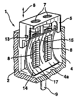
Figures 1 to 8 show a terminal 1 which is part of a
terminal strip 2 which is provided with several terminals
which are all arranged in parallel to one another in the
terminal strip 2. The embodiment shows only the terminal
strip 1 and another terminal strip 3. Since all terminals
have an identical construction, the following description is
limited to terminal 1.
Figures 1 to 5 illustrate that each terminal and also
terminal 1 are arranged in a shaft-type cavity 4 within the
housing of the terminal strip 2, and that an actuating key 5
is held in the shaft guide 4 to be displaceable in the
2 1 76~3 1
....
WO 96/09664 PCT/EP95/03362
direction of the arrows 6. The actuating key 5 has two
openings 7 which have a circular design in the embodiment and
widen slightly conically in the upward direction. These
openings 7 are aligned with two strip profiles 8 made of a
conductive material which are both (see also Figure 8)
connected in one piece with a connection contact 9 designed as
a solder lug. In the area of the connection web 10 to the two
strip profiles 8, this connection contact 9 has a detent 11
and, when the part illustrated in Figure 8 is plugged in the
direction of the arrow 12 into the shaft 4, the connection
contact 9 can be locked by this detent in an opening of the
shaft 4 and of the housing 2 which is not illustrated in
detail. In the same manner, the actuating key 5 also has
laterally projecting detents 13 which have the purpose of
preventing the actuating key 5 from falling out in the upward
direction after the insertion into the shaft 4.
Between the actuating key 5 and the bottom 4a of the
shaft 4, a leaf spring 14 (see Figure 6 and 7) is inserted
which, when inserted into the shaft 4, is prestressed and is
therefore supported by means of its lower end on the bottom 4a
and by means of its upper end on a projection 30 of the
actuating key 5. The leaf spring 14 in this case consists of
two partial leaf springs 14a and 14b which are separated from
one another in their function by a separating cut 15 and are
each provided with two apertures 16 and 17 and are connected
with one another in one piece in their lower area. The
~ t ~
WO 96/09664 PCT/EP95/03362
apertures 16 and 17 have a rectangular construction.
Apertures 16 are constructed to be significantly larger than
apertures 17. The lateral edges of the apertures 16 and 17
are aligned with one another in such a manner that the
apertures 16 and 17 are in each case also disposed below one
another in an aligned manner.
The dimensions of the apertures 17 are selected such that
the upper and lower edges, in each case, engage the strip
profiles 8 when the leaf spring 14, as illustrated in Figures
2 and 4, is placed by way of both apertures 16 and 17 onto the
strip profiles 8. The leaf spring 14 assumes a curved shape
such that the upper edge 16a of each of the apertures 16 and
the two edges of the aperture 17 extending in parallel to the
edge 16a rest against the strip profiles 8.
The strip profiles 8 are designed as conductor guides and
are constructed approximately in the form of grooves with an
approximately V-shaped cross-section in which the ends of
conductors, which are not shown, for the purpose of the
contacting, can be introduced through the openings 7 of the
actuating key 5. The conductor ends will then be in contact
inside the groove guide of the strip profiles 8 and are
pressed, by the edge 16a (see Figure 5), fixedly and securely
against these strip profiles 8 such that the edges 16a do not
rest directly against the strip profiles 8, as illustrated in
Figure 5, but rest against the outer surface of
2 ~ ~83 ~
.~.,
WO 96/09664 PCT/EP95/03362
correspondingly slid-in conductors. Figure 5 also shows
clearly that, because of the arrangement of the separating cut
15, conductors of different diameters can also be introduced
through the openings 7, which conductors can then also be
contacted by the respective edge 16a of the pertaining leaf
spring 14a or 14 b.
The manufacturing of the terminal according to the
invention takes place automatically in a simple manner such
that first the leaf springs in a curved condition are placed
on the assigned strip profiles 8, then the strip profiles with
the placed leaf spring with their connection contact 9 are
slid through the corresponding aperture 17 (Figure 4) of the
shaft 4 until the detent 11 snaps in and then the actuating
key 5 is fitted on which is secured in position by its detents
13, which reach behind corresponding projections of the shaft
4. In this condition, the leaf spring is situated in the
shaft 4 under tension. When the key 5 is actuated, the upper
position of the leaf spring is bent downward (the lower
portion can be fixedly locked on the strip profiles 8 by the
aperture 17), so that its edge 16a, which therefore also forms
the contact member, is removed from the strip profiles 8 and
permits the introduction of a conductor end.
Figure 9 illustrates a modification of the terminal
according to the invention to the extent that no solder lug 9
is connected in one piece with the two strip profiles 8, but
2 1 ~58~ ~
WO 96/09664 PCT/EP95/03362
two contact studs 18 which form a fork-type plug-in device and
are used as connection contacts. However, in this variant,
the contact studs 18 do not project freely out of the housing
of the terminal strip 2 but are held in a housing 2' of a
terminal strip which otherwise is also designed for several
terminals and which also surrounds the ends of the contact
studs 18 which are guided in corresponding slots 19 of the
housing 2~. In addition, the housing 2' has an insertion slot
20 so that slid-in printed circuit boards may directly contact
the contact studs 18. The rem~;n-ng construction of the
actuating key 5 and of the strip profiles 8 arranged in a
shaft 4 and serving as the conductor guide is identical to the
embodiment of Figures 1 to 8.
Figures 11 to 13 show embodiments of a connection contact
similar to Figure 8 or similar to Figure 10. In this case,
Figure 11 illustrates that the solder lug, which may also be a
plug-in pin, is plugged in directly between the two strip
profiles 8 and is connected with these either in one piece or
by welding. In this case, the plug-in pin 21 has the detent
11 for direct fastening on the housing. The design of the
shaft must be adapted correspondingly.
Figure 12 illustrates a variant of the contact studs of
Figure 10 in which the plug-in studs 22 project at 90 with
respect to the longitudinal direction of the strip profiles 8.
In this variant, a direct contact with printed circuit boards
2 t ~
..
WO 96/09664 PCT/EP95/03362
can be achieved by introducing the printed circuit boards
perpendicularly to the feeding direction of the conductor ends
to be connected.
Figure 13 shows a variant in which the contact studs 23
are offset by 180 with respect to the plug-in direction of
the conductors that is, they are arranged in parallel to the
strip profiles 8. A direct contact with printed circuit
boards can therefore take place from the same side from which
the connection of the conductors also takes place. Naturally,
the housing form must be correspondingly adapted to the
contact studs of Figures 12 and 13.
Figure 14 shows the an embodiment in which the two
conductors 24 and 25 have different diameters and can be
introduced through the openings 7 of the actuating key 5 in
the manner described above. From the other side, conductors
26 contact the strip profiles 8 used as conductor guides
through openings 27 in the housing 2 of the terminal strip on
the bottom of the shaft 4 which, in turn, extend in an aligned
manner with respect to the longitudinal direction of the strip
profiles 8. In this case, the securing of the position of the
strip profiles 8 must be solved by separate measures.
However, the strip profiles 8 may be secured in position
by the leaf spring 14 or its parts 14a, 14b with the apertures
17.
6 8 ~ 1
WO 96/09664 PCT/EP95/03362
In the case of the embodiment illustrated in Figure 14,
an edge of the aperture 17 is also used to contact the
conductor. It is illustrated that the end of the conductor 26
is held between the lower edge of the aperture 17 and the
strip profile 8. In the case of this variant, it is
advantageous to press away the edges of the aperture 17, which
at first are in a firm contact, by means of a suitable tool 28
before the conductor 26 is introduced. This embodiment is
particularly recommended when, for example, sensitive and
high-expenditure data processing equipment is to be installed
in areas to which free access exists before the actual final
assembly. In this case, the data processing equipment may be
applied to the terminal according to the invention by means of
corresponding leads (such as 26) so that, at the time of the
final assembly, only the stationarily disposed conductors
(such as 24, 25) can be applied to the terminals in a simple
manner and without any tools.
13