Note: Descriptions are shown in the official language in which they were submitted.
`_ 2178015
B838FCA.doc/specs/jd
MIRRORS AND T~F.~ PRODUCTION
The invention relates to mirrors and to a method of p~ ,c;i~g mirrors.
Eu.~pea~ patent spe~ifiratiQn EP 0 583 871 Al c~esçrib~ps a method of pr~l~,cing mirrors
by appl~lg a coating cc...~ ing a reflP~ting layer and at least t vo reflectiQn enl- n~ g layers
to a ribbon of hot glass, for c~ le a ribbon of float glass, during the glass procl~tic~n
process. The layer rwllles~ from the source of light to be ~l1P~ in use is ~g~ed as the
reflP~ting layer, with the reflçrPon çnh~ ~ç;ng layers being be~ the light source and the
~flf~tirm layer.
The reflPA~ting layer may be a layer of high lcr~;li~e index, for eY-a~ le silicon, a silicon
oxide having a leÇ~ e index of at least 1.9, tantaltlm oxide, tin oxide or t;l ~--;u~.. oxide, with
the rçflP~inn e-.h~n~ h.g layers being altPtra~r~dy of relatively low l.,Ll~li~f, index and high
ef~ t~e index. A reflP~ti~n enhancing layer of high lGrl~cti~e index may be, for example, of
any of the high l~,Ll~ ti~ index matPrial~ listed above for the l~nP~~ layer. However, since
silicon has a higher absorption for visible light than the metal oxides listPd, it is gPner~a.lly
plGf~l~,d, according to the teaching of EP 0 583 871 Al, to use, for a back surface mirror, a
metal oxide layer as the high lGÇl~;li~e index inner reflection çl~h~n- :ng layer in order to
achieve the required high visible light rPflecti- n Thus, in a ~lef~ u~;lw~, for a back
surface mirror, the ~l;.n~".nf nl of layers is
glass
inner (reflection çnh~nring) layer of metal oxide
int .. "~r.,~ate (reflPcliQn çnh~ g) layer of relatively low le~ re index
outer (lGnf~t;ng) layer of silicon.
2178015
The reflection enhq~-ci~g layer of low refractive index may be of silicon oxide having a
~ii~li~,e index lower than that of the ~n~ g layer and that of the high refractive index
reflP~tirn enh~ g layer and in any event less than two.
At least the rPflP~ti~n r~h~ g layers are formed of layers of very app~ ly n~,/4
thir~nrs~ ein n is an odd integer (preferably 1) and ~ is a waveleng~ of light in the visible
region of the spectrum, such that the layers act to çnh~nce the reflection by an int~.relellce
effect.
Mirrors in acco~ ce with the invention of EP O 583 ~71Al have a nulllbel of important
advantages over convçnti~ nql mirrors. Not only can they be produced by applying the
rçflP~ing coating to the glass during the glass prod~lction process (so avoiding the need for a
sepa~le off-line process to apply the reflP~ting coating), but the coating layers may be applied
by pyrolytic processes (e.g. rhrm:~ql vapour deposition) utilicing the heat of the glass to
produce pyrolytic coatings of high durability. Howeva, there is a ten-l~P-nry for the mirrors to
exhibit a reflP~ti~-n colour which is sigJlifirqntly more green than a convçnti~nq-l mirror. This
~ndellc~ to a green reflectiQn generally incleases with in~ as~ reflection (as the thirlrness of
the layers, espeçi~lly the rP.flection enh~ g layers, more closely applo~ q4s to n~4, where
is the wavelength of light towards the middle of the visible region of the S~;llUIII).
Moreover, it is esperi~lly ci~ifir~nt in back surface mirrors where most of the l5illP~d light
passes twice ~rough the Ihir~ .C.C of the glass which may impart a green tint to ~ rd
light as a result of the pl~isel ce of ferrous iron in the glass.
The present ihl~enlor has now found that, through careful selectiQn of the thicL ..~- c~s and
~;fld~ indices of the individual layers of the mirror coating, a back surface mirror having a
visible light rçflç~tion of at least 65%, and, in plere.l~id emb~l;..-el~l~, at least 70% and a
reflecti~-n colour having an a* value of greater than -6 may be produced.
2l7snls
ing to the present invention, there is provided a back surface mjrror co..~l~.;s;ng a
glass s.~ t~ carrying a reflPcting coating co..~ ;n~ a l~nP~ g layer and at least two
rPflP~tinn enhancing layers, the thi~L ~S~,S and ~Ld~ e indices of the layers of the coating
being eele~tP~ to provide a visible light rçfle~tif)n of at least 65% and a refle~tinn colour having
an a* value greater than -6.
The eA~)~ssion "visible light reflP~ on", as used in the present s~;r~ on and claims,
refers to the pe~ ,l~ge of lightreflected under nl.. ;~ D65 source 1931 Ol,s~
Con lition~ The reflPrtinn colours referred to in the present spec;firq~tion and claims and
defined in terms of a* andlor b* values are colours defined in accof~ ce vith the CIE system
(ASTM nesig~q~;nn E 308 - 85), and, as quoted, are ll~as~id using n~ t D65 source
1931 Ol,~l~.l Con(~itions
Back surface mirrors according to the in~,e.l~n preferably have a visible light r~llf" I;m~
of at least 73%.
Back surface m~rors accol ihlg to the invention p~rerably have a ~flectiQn colour
having an a* value greater than -5.
The glass substrate may be of float glass and will normally, but not nP~S5 v ;ly, have a
thir~npsæ greater than about 2 m~ and less than about 12 mm. For most ap~ qtions
reqlliring si~ir( ~ll mjrror areas, the glass will have a nominq,l th; ~n~ss of 3 mm or more.
As in the invention of EP 0 583 871Al, the lGnP~;~h~g layer is a layer of high l~fl~i~e
index, while dle rçflPcti-~n çnh~nfing layers are altPrn~tPly of rela~ively low and high leli~li~e
indices. The f~ g layer is the layer which is, in use, furthest from the source of light to be
reflP~teA, and ~ e rçflPcti~-n çnh~n~ing layers are between the light source and the reflection
layer. It will be appreciated that the reflecti~ n enh~ ng layers may reflect more light than the
l~llç~;ng layer.
~ 2178015
The thir~nPs~ of the reflPction enhvq~ing layers may be sele~l, in generally known
n~qnner~ so that reflechion~ from the i~ . ri--,es ~1~.~n the reflPctirm enhq~ing layer ndjq,^,P-nt
the glass (i.e. the inner reflPcti.?n e -.h~ri~lg layer remote from the ~ c~ g layer) and the
glass and ~h.~n the two reflP~hi~m enh~ri~g layers l~ rul~ reflection~ from the face of the
rGflPrting layer adjacent the int~rn PAiq~e rPflPch~-n enhqnring layer. This will occur when said
inner and intPrm-P~ q-t-P, rPflP~tion e--h~ c;~g layers each have an optical thirLn-p~ss of about n~4
W1h~1G~ in each case ~ is a wavelength of light in the visible region of the S~ Unl i.e. about
400 nm to 750 nm, and n is an odd integer, n may be the same or dirrYl~,nt for each of the said
layers but is preferably 1 in each case.
The ~ L -f ;~ of the lc-~ g layer may similarly be selPrtP~ so that reflP~hion~ from the
face of the reflPction layer ^ lj~q~--pnt the ;.,~ - - -PAiqtP rP~flpctil~n enh ~ g layer (i.e. the
interface bet~ . ~n those two layers) are reinrc~l~ by rP.flection~ from the outer face of the
reflPching layer. Unless the outer face of the ~efl~Y~ g layer is in cont ct with a layer of even
higher ~L.~;Ii~e index, this will occur when the optical th;~nPss of the rPflPcti~ n layer is
about n~4 wL~.clll ~ is a waveleng~ of light in the visible region of the s~u... and n is an
odd integer, n~rmqlly 1.
The desired high visible light rYflPction is most readily achieved, while avoiding an
-n~les;.~bly Shrong green tint in the 1Y~ ;O~ colour, by using silicon for both the refl~Pcting
layer (i.e. the outer layer of the reflecting coating) and as the inner (closest to the glass)
reflPcti- n e~-h c;~-g layer.
To control the teml~ nc~ to a strongly green reflection colour, while at the same time
lg a high light r~flectiQn, an inner r~YflPcti~ n Ç.~h~.u`;.~g layer of optical th~ np~ss less
than 125 nm rnay be used and it is plcfellcd to use an inner reflPcti- n Pnh~n~ing layer of
optical th;r~s~ less than 100 nrn, and espe i~lly less than 90 nm (but more than 50 nm).
,~. 2l7snls
A particularly pfcÇell~,d inner reflection enh~c:ng layer is a layer of silicon having a
thi~nes~ in the range 14 nm to 19 nm
The optical th;cLness of the refl~ting layer is gen~r.qlly less critical than the Ihi~L ~f cc of
the refle~on ç~lh~ g layer, but will ~rrnqlly be over 100 nm and, in order to control the
loss of lig_t by absoIption (esper;qlly when it is of silicon), less than 150 nm In practicc~ it is
found that in.;.~ g the optical thicL-ness of the silicon lclh~;l;n~ layer, while ..~ in;n~ the
thirlrn~.ss of the refl~.ctiQn enh~nrin~ layers, tends to reduce the green tint of the rçfl~tior.
colour, ie. ncl~ase a*, and a less green refl~tion may be achieved by using a silicon n,rlf~ g
layer with an optical thirL-ness greater than 125 nm.
A particularly p~ f~ ,d reflecting layer is a layer of silicon having a ll,i~L .~ss greater
than 20 nm and especi~lly a th;cL-n~ss in the range 25 to 35 nm..
The refractive index of silicon may be as great as about 5 (see P J Martin, R P
Neth~ l, W G Sainty and D R McKen7ie in Thin Solid Films 100 (1983) at pages 141-147)
although lower values are often encou"t~l~ d.
It is L nown in the art that refractive index varies with waveLong~h In this spe~ificr~ n
and claims, references to ".~,rla~ e index" are int~n~letl to mean, in coll~e ntion~ ~r, the
~i~.e index for light of wavelength 550 nm (and, for the avoidance of doubt, it is hereby
co~r~ ~at the optical thi. - ~.es~es l~irell~d to herein are optical th - ~es.~s c~lcu~ d from
the lerl~li~e index for light of wavelength 550 nm).
It is believed that, in p~c~;ce, the 1~ rld~ e index of silicon varies ~pen~ling on the
precise physical form of the silicon and the presence of any ;-~p~ es, for e ~ qile oxygen,
nitrogen or carbon. For the purpose of the present invention, the presence of such h~ s
may be tolerated (and indeed, it is rliffirlllt in practice to produce on-line silicon co~ting~
without sigl-ifirPnt oxygen and/or carbon incorporation) provided the le&~;li~e index is not
217801~
. ~ 6
reduced below about 2.8. Thus the tçrm "silicon" as used herein with l~fe,~"lce to layers of
~,lati~_ly high refractive index refers to mqt~.nql which is pre lo~;nq~llly silicon, but may
contain minor plo~ ions of h~ ies, provided its leii~;li~_ index is at least 2.8; ~n,f~,dbly
the ~li~;li~re index of the silicon used is at least 3Ø
To achieve the desired reflP~tion and colour, with the thin inner ~: n~ g e nl~
layer r~f~ d to above, the inle~ffA;-qte reflecti.-n e .-hAl-. ing layer adjacent the rçflP,c~ing layer
may have an optical thi~L-nPss greater than 125 nm, and it is pl~,fe,l~d to use an inh~.~r~ t~
reflPcti~ n e--h~-u~;,-g layer of optical ~ L np~ss greater than 140 nm (but n-~rmqlly less than 200
nm).
The rP.flP~ti-m enhancing layer r1j~nt the ,eriecl;ng layer should be of relatively low
~,L~1i~. index, ~Pnerqlly a refractive index of less than 1.8 and preferably a lef~ e index of
less than 1.6. For a high visible light rPflP~tion, it should be of a material which is s.lbs~-q ~tiqlly
non-absorbing in the visible region of the ~ unL A suitq~lP and con~ t layer m~ter~l is
silicon oxide, which may however contain minor prop~ons of ^ 1(1iti-~nql P1~ "~ such as
carbon or nitrogen, and the term "silicon oxide" is used herein to enco~ C~ silicon oxides
co~ g such i...l.--- ;I;~s~ However, in order to obt, in a high light 1~ C' ~m it is plef~ d
to use a silicon oxide with a ~ilicon oxygen ratio app~ ~ely 1:2 and a low level of
s such that its ,~,rl~~ e index is below 1.6 and pne~lably below 1.5.
A particularly pl~ ,. e~ e reflectic)n e--h~ g layer is a layer of silicon oxide
having a Ihi~L~ess in the range 95 to 130 nm, although other m~t~.ri~l~ of suffiri~pntly low
e index, for example ~1-..";";~.." oxide, can also be used.
As in EP 0 583 871 Al, the layers of ~e ~ cd lGr,~li~. index may be applied to a
ribbon of hot glass during the glass pr~duction processes by pyrolytic proGesses It is gPnP.r~lly
con~e.~"l to use a c~ l vapour deposition process to apply any silicon or silicon oxide
`~ 2178~15
layer that may be Iequired. Thus, for example, a silicon layer may be deposit~l (directly or
hl&~:~) on the hot glass Ubstr~t~ by çh.~.m;~l vapour depositiQn from a silane gas,
conveni~.l~ in a gaseous diluent, for e~ nitrogen. It is generally most con~e,~ienl to use
monosilane, although other silanes may also be used, such as dichlorosilane. One suitable
process for ~positi~m of such a silicon layer is desrribed in GB 1 507 996. If desired, for
example to improve the alkali resi~t~l-ce of the silicon co~ting, the ~ gas may contain a
p~ ion of a gaseous ele~lloll don~ting cGIly~oulld, espe~ i~lly an etl,yl~l-ic~lly ullsalul~d
hydloca l,on compound, for example, etllyl~lle, as additive (although use of high plopollion of
such compoullds will nonn~lly be avoided as their presence tends to lead to incorporation of
oxygen, believed to be from the glass, into the silicon coating with con~u~nt reducti-)n in
refractive index).
A silicon oxide layer for use as a refl-o~tion çnh~ncing layer of low refractive index (i.e.
an i ~- ..R liate layer) may similarly be depGsild by çhf ..ical vapour depos;~i~ n from a silane
gas, COI ~e.~ienlly in a gaseous diluent7 in ~ with oxygen or a source of oxygen. A
n~lu~ of a silane and an elllyl~nicdlly w~salu~a~d hydrocallJon~ together with carbon dioxide
or an ~lt~ . ..;.l;~, oxygen compound which serves as a source of oxygen such as a ketone, for
example 3~eton~7 may also be used. The relative conc~ntrations of silane and the source of
oxygen used will depend on the IGrla~ e index required; in ~.n~ l, the lower the ~er~ ,e
index ~quil~d, the larger the plopol~ion of oxygen-cQnl~in;ng colll~oul~d to silane to be used.
Again, the silane used is preferably a mc)nosil~n~
When applying a coating layer to a ribbon of float glass, the chemic~l vapour deposition
tGchl-i.lues can COll~e-~lltly be caTried out inside the float bath i.e. where the glass is
supported on a molten metal bath under a protective ~sphere (but preferably after the glass
has r,~ s~bching i.e. at a glass ~nlpe.alule below 7509C), or after the ribbon has
2178015
e,l~r~;ed from the float bath. When using a gas COI~IA;~ ;ng mono~ A.IP, to deposit silicon or
silicon oxide layers, it is plefe.l~id to carry out the deposidon of those layers in the float bath
where the glass is at a t~ u~ e in the range 600QC to 750QC in order to achieve a
sadsfactory rate of deposition.
The p,ef~ ;d silicon and silicon oxide layers used in the pl~tirA~ of the present
h1~e~ n~ while l~n~,;i~g in the visible region of the ~ 1UIII, are subst~Antiq1ly ~ ~AQ'~ in
the infra red region so that their presence (unlike that of layers of silver tr~;litionqlly used for
mirrors) on the surface of the glass during ~ Alin~ wiU not have any s.lbst~ ql del~ IA1
effect on the q~nPqling of the coated glass. This means that such mirrors can readily be
produced on-line in a float glass process with the miIrors being ~nnP~lPA in known ...~ u-e..
According to a further aspect of the present invention, there is provided a method of
producing back surface milrors compri~ing depositing onto a ribbon of hot glass during the
glass pro~h~;nn process two refl~ction enh~ layers followed by a refl~ctin~ layer the
reslllti~ m-irrors have a visible light rcfl~ction of at least 65% with a refl~ction colour having
an a* value of greater than ~.
The pl~.f~ d silicon and silicon oxide layers used in the rnirrors of the present invention
have a high degree of che-~ic~l durability, so that, in contl~st to con~e.-lional silver miIrors, the
mirrors do not require ~ Afl protection by a b~r~ing paint. However, silicon has limited
scratch l~ s:~A~-re and, if desired, an ~i~liti- nql protective layer, for e~ ,lr. of metal oxide,
espec iqlly tin oxide, may be provided over the reflecting coating. This may conveniently be
done by a pyrolytic coating technique applied, after deposition of the l~ g co~ting~ during
the glass prod.,cl;on process. However, care may be ~ui~ed to avoid the contlitil)n~ l~ui~d
~1~1. ;"~ ntAlly ~ffPcting the pl~opelli~s of a silicon lellec~ g layer and it may t~hus be appl~pliale
2178~15
to delay applic~qtion of the protective tin oYide layer until after a surface layer of silicon oYide
has been found on the silicon, for eYq-mp4 as describPcl in US patent 4 661 381.
The mirrors of the present invention are useful for a wide range of purposes, inclll~ling
domestir use as mirrors in bathrooms and bedrooms. For many uses the mirrors wiU be
provided vith an obsc~ iayer, preferably a s.~l,s~ ll ;qlly opaque layer, over the l~,llP~ g
coating.
Thus, r ~c ~ ~ding to a ylefe.~,d aspect of the present invention, a rear surface mirror of
the invention ~ tionqlly co- - .l-. ;~s an oy~irying layer. The Op~i~yil~g layer may be a paint
layer or a p,efo,ll~d .~.f ~ assembled against the coated glass.
When an opacifying paint is used to form a paint layer, it may be an aUcyd resin based
paint, cptionqlly co~ ing an amino resin, for e~ ~,q)lf, mP1qminP~ and may have an organo
silane primer incoly~ated therein. The paint wiU n-~rrnq-lly contain an o~ily"~g agent, for
eYample carbon blacL~, preferably in an amount of at least 1.4% by weight, based on the weight
of the dried paint. Because the refl~cting coatings of the present invention are çhPm; ~lly
d~l~blc the paint may be lead-free.
The mirror co~qtings of the present invention are preferably deposited on a hot glass
ribbon on-line during the glass production process. The coated ribbon is cut on-line to form
individual mirrors, and wiU usuaUy be further cut off-line to provide ~p~ ,~b, mirrors of the
,d size. An op~irying paint, which may be solvent based or water based, may be
apylied off-line, convel~ell~ly by a curtain coating process or a roUer coating process and
preferably before further cut~ng of the mirrors off-line. ~lt~rnqtively, the opa~ily"~g paint may
be applied on-line by a spray or roller process. RP~flme the paint is not required to provide
chemical durability, thin paint layers wiU suffice, so that paint layers thinner than 50 mi~
and pl-,f~lably (for e~onQmy) thinner than 25 ".,~.~ns may be used (the Ih;('L n~SS speçified
2178015
being dry ~ L ..~ss), a typical as-cured or dry ll.icL .~es.c being 18 to 30 microns for curtain
coated paints and 15 + 5 ".i ;,ons for roller or spray applied paints.
A primer layer may be applied to the mirror coating before paint is ~I~pli~ or the paint
may have a primer il~cc~ a~l into the conlI~ositil)n thereof. A slliPl l~ primer is an organo
silane, and a particularly suitable primer for use with aLkyd based paints is an or~,qnosil ~ ~e
having amino end groups, such as an qminop.~pyll. ;...~tl.l xysilane. That primer is stable in
water and wets the underlying surface to be pqint~d It may be applied as a 1-2% aqueous
solution in de;c.ni~ water. ~lternqtively, when the organo silane primer is i~c~l~ol~tcd into
the paint, the primer is preferably present in an vq~nollnt of from 1 to 6% by weight based on the
weight of the paint at a typical solids content of around 62%, most preferably around 1% by
weight. The applir~qtion of paints to mirror coatingl~ of the kind generally described in EP O
583 871Al is more fully ~ sul in WO 95/18774.
~ lt~r~ vely~ the opa~iry--lg layer may be in the form of a pl~,fol-- ed n~mh~r assembled
against the coated glass. Such a pl~;fol.-~d ~mber may be a plastics film adhered to the
coated side of the mirror, or may be a sepdl~t~, ply assembled against the coated side of the
glass, for e~ le a board having a dark, e.g. black painted face, against the coated glass.
In the pr~dnction of mirrors according to the invention, a coated ribbon may be cut on-
line to form individual mirrors, and will usually be fur~her cut off-line to provide ~i~
mirrors of the required size. The opacifying ..~ ...ke~ may be ~emh'cd onto the mirrors off-
line preferably before further cutting of the miIrors off-line.
The op~ifying "~.,.kf . plcrclably co..-~ .;.~s a self-adhesive plastics film (enabling a
safety backed product to be achieved). The plastics film is ~n~lucent or opaque and carries a
tr~n~lll~nt or (when the film is tr~n~ ççn~) an opaque p~cs~ sen;,ili~e adhesive. Carbon
black is pl~f~ably present in the adhesive as an Op~,ir.., . The adhesive is preferably an
2178015
11
acrylic-based adhesive. The plastics film is preferably a polyolefin film, such as a film of
polyethylene or poly~ p~lene, and is preferably biaxially oriented. Such biaxial o. ;~
can enhance the impact pe. rO. . . ~ rc of the safety backed mirror. Alternatively, the plastics
film may co.-y~ e a polyester film. The films may be clear and tran;,~ t, or coloured. A
st plef~-~d film is a poly~l~ylene film c~urying an acrylic adhesive which in its p~
s~ , form is known for use with. polyester films employed for use in i llp~ing bomb-blast
protfxtion or solar control to ~5157.i~g.~, which adhesive is known to be co--~p~;b~e with glass.
A typical self-adhesive film has a total thirL-nP~ of around 90 microns, the plastics film and the
adhesive having ,~ e a~pro~;..k~ thi~L nPs~s of 60 and 30 Ill-crons.
The adhesion bel-. ~n the rear surface of the mirror and the self-adhesive plastics film
may be enh~r,ed by the use of a primer which is applied to the refl~cting coating before the
application of the self-adhesive plastics film thereover. The primer is preferably an
org~nn~ f ~ preferably having amino or epoxy end groups, and in particular the primer may
be amir,opl~p~ hoyysilane in aqueous solllti--n That primer is stable in ~ ;o--;~ water
and wets ~e underlying surface to be covered by the self-adhesive filnL It may be applied as a
2% nqueou~ sol~ltion in deioni~ed water.
In an ~ltf~rn~tive embodiment of the present invention, the Op;~iryillg ..~ .~.kr co...~ ,s
a sep~ ate lamina having a face assembled in contact with the back surface of the mirror.
~eÇe~ably, the opa~;iÇy~lg -~---be~ of the mirror assembly conlrri~,s a board having a d -~f~n
snrfare, most pl~;Çelably a matt sllrf~e, which is A~m~ for eY~le, by the use of fr~m;ng
...f ..,h,.~ or other .~ ic~ r~ f nl~i to the back surface of the mirror. The board may
for e~ le conlrri~ hardboard painted with a black matt paint with the painted surface
asse.~ble~l, for a back surface mirror, ~j~çnt to t~e reflPcting coating of the mirror.
ely, the op~irying .~ l;f r may conlrri~ black paper.
2178015
12
In each of those sperifi-p~l embo~ n~c, the opacifying n~c~ is qQQP.mbl~P~ together
with the glass s~s~ carrying dle lçnf~ g coating to form a unitary rni~ror ~--..bly as a
conlrosit~ bly. However,inafurther~q,~ çmbo~ enttheop~i~ g ~ fr
may c~.~ ;~ a wall of a b~likling~ preferably having a ~ l surface adjacent the m~ror,
and the mirror assembly of the present invention cc..~ ;~s the glass s~ t~, carrying the
cnP~ g coating q-QQPmhl~d onto the wall. The use of opacifying ...r..,,h~"s in mirror
assemblies in which the l~nP~l;,.g co.~ tingiQ- may be of the kind generaUy described in EP 0 583
871Al is more fully (~iQ-cllQse~l in WO 95/18773.
Re~lii~g to the s~ ule of the lçn~ ; -g coating, the skilled man will applec;dle that
itionql low and high refractive index quarter wave (n~/4, where n is an odd integer,
preferably 1) layers may be added to the stack of layers forming the refl~P~ting coating to
further e -h~ the rçflP~tion
It may also be possible to incol~ol~t~ litionql non-quarter wave layers ~t~.~n the
said inner and outer layers, although in that event such layas are generally best n~gdl~ed as
forming part of a cQn~rosit~ i~t~-rrn-pAiq-t~ layer which should, con~i~lçred as a conlrosit~ single
layer, have a thirlrnP.s~ such that the phase differences of the light reflP~t~d from the intPrf ee
of said c~nlrosite in~rmerliqte layer and the inner reflection e--h~n~ g layer ~eillfo~e light
~ d from the in~,. r~ce bet..~.l the composite jl,h ."~l;q~ layer and the reflecting layer.
Simi1qrly, an ~lditionql laya may be inrlllded be~ the inna laya and the glass although it
will then n~ rmqlly be of l~ /e index il.t....-~Ai^~ belw~ll the refractive index of the inner
layer and the glass.
The invention is illllstr~q,hv~3 but not limited by the following srl~ drawings and
des~ n thereof and the following Fy^ nplPs~ In the drawings:
Flgure 1 is a section th~ou~;l, a mirror in accordance with the invention.
13
Flgure 2 is a section through a mirror as illustrated in Figure 1 with the ~qd~lition of a
protective layer, or an opdci~rhlg layer in the form of a paint or plastics film, over the ~nec~ g
co~
Flgure 3 is a section through a mirror as illustrated in Figure 1 with the ~ditif~n of an
Opd~ g layer in the form of a sepala~ ply over the lefl~ g c03ting
Flgurc 4 is a rep~ n~ ;on of the aTrfi~ ~ of coating st~q-tion~ on a float glass
produr,ti-n linc for p,o~lucl;on of miTrors in accordance with the method of the present
invention.
Figure 5 is a section through a gas rliQ1ribu~)r suitable for use at any of the coating
stations 15, 16 and 17 indi~qt~ in Figure 4 for depositing a layer of the rP,flPcting coating used
in the present invention by ~hem:-a1 vapour deposition.
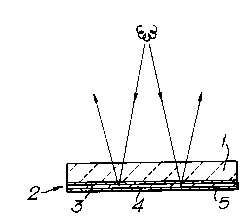
I?pfçrring to Figure 1, a back surface mirror compri~P,s a float glass substrate 1 carrying a
lc~ g coating 2 con~rriQing an inner reflP~tion enhqr~ g layer 3 of silicon, an i~ . " ~
reflP~ti~n el~h~r;ng layer 4 of silicon oxide and an outer reflPction layer S of silicon. The
layer l~ es may be as d;~-u~sed above. The produc~ic)n of such mirrors having a visible
light reflection of at least 65% and a refl~P~tion colour having an a* value greater than -6 is
des rihPd in thc following Example.
In Flgures 2 and 3, the same numerals are used to desi~qb~ the same substrate and
layers as in Flgure 1. In ~l~lition Pigure 2 shows an q~Yitionql layer 6 which may be a
protective layer (for example a thin layer of tin oxide) or opacifying layer in thc form of a paint
layer or self-adhesive plastics f~ (when layer 6 is an opacifying layer, it will ncrmqlly be
subst-q-nti-q-lly thicker than the other layers shown). ~lgure 3 shows an Opâcil~ulg layer 7 in the
form of a board which preferably has a clA-L~ surface adjacent the glass assembled by means
of a frame 8 against the coated surface of the glass.
2178`01~i
Figure 4 illustrates tlia~;.. " ~ir~lly a float glass p~odu~;~ion line cfJ...~ g a glass
n~Plting secdon 11, a float bath section 12 for fo""ing the molten glass into a continllous
ribbon, a lehr section 13 for ~nnP~ling the said glass ribbon and a warehow section 14 for
cutdng pieces of glass from the ribbon for storage and/or distribution and use. For the
producti- n of mirrors in acco~dnce with the invention, each of the three coating s~ion~ for
~,s~ ,ly applying the inner, in~ . ..P~ , and outer layers will nl)rm~lly be located in or
bel~n the float bath section 12 and lehr section 13; in the illll~tr~tP~ embodiment of the
invention~, the said three coadng stations 15, 16, 17 are arranged in the float bath section 12 as
shown in Figure 4. The locqtion of each coating station is sfle~t~l to be at a position where
the glass ribbon has s~lbst~nti~lly ~h~ its final thir~ness (usually below a glass t~ e~u~e
of around 750QC) so that it is not subject to further ~llclchil~g which might crack any coating
layer ~r~pli-P~, but (at least for the inner and in~ tJ~ layers) where its ~."~a~e lG.I~ins
s~lffi~Pntly high for f~tic n of a further pyrolytic layer.
E2~Pferring to Figure 5, a dual flow coating gas distributor beam, genP,~lly ~Psigr f~ed 20,
useful for the p~ ;ce of the present invention Co",plisGs a rl~ wo,k 21, formed by spaced
inner and outer walls 22 and 24, dçfining enclosed cavities 26 and 28 through which a suitable
heat eyGh~ngp ...~.1;...~ is circulated for ~ ing the distributor beam at a desired
e-~ ,. Gaseous p,~ rs supplied through a fluid cooled supply conduit 30 . xtending
along the rl ib~l~o~ beam are -1mitted through drop lines 32 spaced along the supply conduit
to a deli~ cl-~ ber 34 within a header 36 carried by the Ç1~IIGWO~I~ 20. E~ ~r gases
~-~-;lt,d through the drop lines 32 are discllarged from the delivery ~ ,r 34 through a
pa~g~way 38 toward and along the surface of the glass 18 (shown in the form of a ribbon
flo~ting on a bath of molten tin 19) both up~he~n and dow-ls~ (with respect to the
direction of ribbon mo.e.~nl) in the direction of the arrows in Figure 5. Baffle plates 40 may
217801S
be provided wi~in the delivery ch~ be- for equq~ g the flow of pl~-ul~ materials across
the distributor beam to assure that the mqt~riql~ are dischal~ed against the glass in a smooth,
laminar, u- :rc .... flow entirely across the beam. Spent pl-A;ul~ol m ~t~vriqls~ as well as a certain
amount of the surrounding ~t~sphere around the beams, are collP~tP~l and removed through
eYhq~l~t ç~ "~.e ~ 42 along the sides of the distributor beam. Various types of suitable
distributor devices for ch~Pmir~l vapour deposition are g~onP,r~lly known in the prior art as
disclosed, for ÇY?~plP~ in US Patents Nos 4 469 045, 4 504 526 and 5 065 696.
The following FY?rnples illustrate the present invention without l;.~.;l;,~g it. In the
Examples, mirrors were produced on-line using a float glass producti-n line having coating gas
distributors arranged at the coating st~tiQn~ 15, 16 (2 distributors) and 17 shown in Figure 4.
In the F-Y~ S the gas flows where stated by volume are n~.ued at ~ P l~ te~
and a pless~e of 1 bar, and all gas flows are quoted per metre width of ribbon coated.
r..~
Glass mirrors, for use as back surface mirrors, were produced using a laminar vapour
coating process. Four se~ , equi-spaced coating beams as illu~llaled in Figure S were used
to apply s~cess;~e silicon (1 beam), silicon oYide (2 beams) and silicon layers (1 beam) to a
ribbon of clear float glass having a thir~np~ss of 4 mm and advancing at a lehr spced of 555
metreslhour. Each of the coating beams was located in the float bath where the glass ribbon
was s..ppo~d on a bath of molten metal, with the u~ e~l (with ,~ife,,~,nce to the direction of
glass advance) beam located at a position where the glass lr....l~,nn~ was applo~ ly
710QC.
2178015
16
The four coating beams were fed with the gas ~ UlGS shown below:
SiH4 Ethylene o2 N2
1 (Up~,tlGa ll) 1.3 120
2 2.0 12 8 150
3 2.0 12 8 150
4 (Da ~. .,sl,~n) 6.5 1 - 120
No modific,q,tinn of the lehr con~1ition~ was required to anneal the res~llting coated
ribbon, which had a highly reflP~ing appe~ ce. Individual mirrors were cut from the ribbon
by cutting in convçntion^l fashion and the optical pr~pcllies n~,u.~ using an nl...~ D65
Source 1931 Observer Conditions on the ~ co~t~ ~ side of the glass with the following results.
The visible light reflçctil n was found to be 73.5% with the reflP~,d light having an a* value of
-5.1 and a b* value of +0.6.
The a* value was so.l~.l.a~ lower than the ~,er~.l~ ..,h.;.,.~ . value of -5, but (in
colllmon with the other optical plo~l~ies ..R~ c~) was in good a~~ .n~ with the value
c-q-lr,ul~ for a coated glass having the observed combination of layer thirL nPss and ~L~ ,re
indices (the inner, reflçction ellh~ ,ing layer had a thi- L-nP.ss of 18 nm and a leL~;li~e index of
4.4; the i~ ;qte~ rcflPction çnhqnc in~ layer had a thi~L-nçss of 105 nm and a re~i~;li~e
index of 1.46, and the outer, reflPction, layer had a lh;rL ~ss of 19 nm and a lGL~li~G index of
4.3). The same theory predicts that, for a coating compri~ing an inner, reflection çnhqncing
layer of silicon of thirLnP.s~ 18 nm, an i~.t~ Ai~l,e rçflPction enhqn~ing layer of silicon oxide
of ~h-cL ~SS 1 10 nm, and an outer rçflPcti~ layer of silicon of thicl~ nPs~ 25 nm and with the
refractive indices of the layers being as .~l~;;r.~ above, the co.l~,spon-ling values would be:
i~ 217801~
17
Visible light rçfl--cti-)n 74%
a* -3.8, b* +2.3
showing that ~e plef~ d co.~tings of the invention may similarly be produced by minor
modification of the layer ~ L ~,sses.
A milror produced ~ lly in accordance with the above Example (~ving a
visible light reflecti-)n of 74% with a* -5.0, b* +0.9), was backed with a 200 micron black
polyc~ ; film c~l jillg a plcs~ sensitive solvent based acrylic adhesive applied over the
coe~ing Ihe application of the b~ing results in a small change in the optical propellies and a
~as~ucd visible light refl~ti(m of 72.5%, with a* -5.6, b* +0.1.
Thus it can be seen that the present invention permits the on-line prod~lction of back
surface mirrors of high durability, and having a reflPction colour close to neutral and close to
that of a con~e--lion~l silver mirror (a* = -2.5, b* = +1.5, when formed on the base float glass
used in the folcgoing Example).
FY~m~1e 2
The pl`~lulc of F~-nrle 1 was l~ ~-1 except that the 4 mm clear float glass ribbon
was a~ ccd at a lehr speed of 690 metres~our, that dual flow beams 1 (upsllcalll)~ and 4
(dow~ hGa~) were replaced by uniflow laminar coating beams of the kind ~les~ribed in EP 0
305 102B, and dual flow beam 2 was replaced by a n~lified version of such a uniflow laminar
coating beam in which ~e water cooling is replaced by oil cooling, the graphite blocks by
metal blocks, and the gas fiow res~Tict~r by a sequence of baffle plates collc;,pon~ling to that
used in the dual flow beams. The gas flows were as shown below (quoted in litres per minute
2178015
18
for beams 1, 2 and 3 and kilograms per hour for beam 4 except for acetone in beam 2 which is
quoted in cc of liquid acetone per minute):
SiH~ Ethylene Acetone O2 N2
1 (Upstream) 1.4 23
2 5.7 11.4 4.4 19.6
3 2 12 8 149
4 (Dc,~ ) 0.36 0.029 2.6
The res llting coated glass had a visible light refl~ m of 70% with the reflect~d light
having an a* value of -5.8 and a b* value of 0.7. The thi~L ~.esses and refractive indices of the
individual layers were 19 nm, 4.4 (inner ~eflection çnh~n~ing layer), 80 nm, 1.46 (i~.t,. ..~AiAIe
refl~ n ~..h ~ layer) and 25 nm, 4.3 (~ layer).
Exam~le 3
The pl~a; ~ ~re of Example 1 was l~ 1 except that the 4 mm clear float glass ribbon
was ~I~ ced at a lehr speed of 750 metres/hour, that dual flow beams 1 (u~s~ ) and 4
(dow~ ll) were repl~ced by uniflow laminar coating beams of the kind des~ibed in EP 0
305 102B, and the gas flows were as shown below (quoted in litres per minute for beams 1, 2
and 3, and Icilograms per hour for beam 4):
SiP~ Ethylene 2 N2 + He
1 (Upstream) 1.6 23
2 2.6 15.4 5.1 74 + 74
3 2.6 15.4 5.1 74 + 74
4 (Dc,.. lshGam) 0.6 0.31 2.6
2l7snl~
19
The reslllti~ coated glass had a visible light reflection of 73% wit-h- the refl~ct~d light
having an a* value of -2.6 and a b* value of +3.2. The thi~ ~ ~.esses and ~,fl~cli-e indices of the
individual layers were 18 nm, 4.5 (inner refl~cti- n enh~-ring layer), 101 nm, 1.45 (j-,t.....
rçfl~ti-~n enhancing layer), 30 nm, ap~ ately 4 ( efl~ g layer).
Tn.;.~ ng t-h-e ~ L ..~..c.c of the silicon refl~cting layer (co~ , Examples 1, 2 and 3) not
only i~ ,~s the a* value (so that it be,co..~s less neg~ e), but also il~ea~s the b* value.
Market research has shown that incleased b* values are readily ~cept~ble to the co~ n~,,
and ~ ~,Çel-~,d mirrors in acco~ lce with the invention have a* values in the range -4 to -2, and
b* values in the range 2.5 to 4.5, preferably accomp~ d by a light reflection of at least 72%.